Photovoltaically self-charging cell (PSC), a device integrating both a photovoltaic part for solar energy conversion and an energy storage part such as a lithium ion battery or a capacitor,[1–8] has attracted great scientific and technological attention due to the increasing demand of green energy and the tendency of miniaturization and multi-functionalization in electronics industry.[9,10] For the photovoltaic sections of these PSCs, the dye-sensitized solar cells (DSSCs) are frequently used due to their high efficiency and low cost.[11,12] Recently, Guo et al. reported a power pack with a shared TiO2 nanotube functionalized electrode utilized to integrate a DSSC and a lithium ion battery, which achieved considerable energy conversion and storage efficiency.[6] Such PSCs contain three electrodes, the switching among which could realize the multi-functions of energy conversion, storage, and output. Most of the PSCs are of such three-electrode type, which is equivalent to two devices: a solar cell and a capacitor or battery.[1–8,13] However, the control of electrode switching consumes extra energy and increases the cost of the fabrication. Another type is the two-electrode PSC, a simplex device.[1,2] Such kind of PSC could not provide continuous power output after being fully charged under steady illumination. Another problem of such PSC is the poor photo-to-electric conversion efficiency (η), which is lower than 1%.[13] To date, a simplex cell with both photocurrent output and energy storage functions has not been reported.
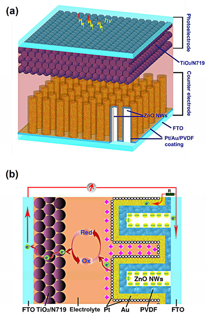
Si powder/poly (vinylidene fluoride) (PVDF) composites have been used as active materials to fabricate a two-electrode photocapacitor and revealed outstanding photoresponse, rechargeability, and long-term storage properties.[2] In this work, the counter electrodes (CEs) of DSSCs are modified by PVDF/ZnO nanowire array (ZNWA) nanocomposites for the energy storage function owing to the high dielectric constant of PVDF and the high surface area of nanomaterials (Fig. 1a).[1,14] The Pt/Au catalysis layer for DSSC and the charge storage interface share the same surface of PVDF coated on ZnO nanowires. The photon-generated current is divided into two segments at the fluorine-doped tin oxide (FTO) substrate: one via the paths formed in the PVDF/ZNWA nanocomposite (represented by a resistor R) to the Pt layer for the photoelectric conversion; the other along and through ZnO to the surface of each nanowire as shown in Fig. 1b. Part of the Li+ in the electrolyte could be attracted onto the Pt surface or embedded into the space between PVDF particles through the electric polarization of PVDF by the electrons on the other side. The stored charge density is up to 2.14 C g−1 based on the mass of PVDF, while the highest η achieved for such a cell after being fully charged could be up to 3.70%. Such cells have a great potential for applications in low-power consumption devices, such as sensor networks, which need to operate all day, continuously and unattended.
Figure 1.
Schematics of the (a) structure and (b) mechanism of TiO2 dye-sensitized solar cell with energy storage function by modifying the CE with PVDF/ZNWA nanocomposites.
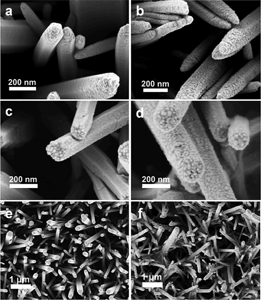
The structure of our PSC consists of a photoelectrode of dye-sensitized TiO2 nanoparticles and a PVDF/ZNWA nanocomposite modified CE, as shown in Fig. 1. In this work, we first established an electrically conductive Au layer by a sputtering process on the surface of PVDF coating, followed by electrodeposition of Pt catalyst on the Au layer, since in our experiments, devices with Au layer alone displayed very poor catalysis to I3− redox reaction. For electroconductive Pt/Au coating on PVDF/ZNWA nanocomposites, there are some discontinuities formed (e.g, cracks and pores). As shown in Fig. 1b, the Au layer is connected to the FTO substrate via R, which corresponds to the paths formed in the PVDF/ZNWA nanocomposite. When the cell begins to operate, photo-generated electrons from the photoelectrode go through the external circuit to the CE. Subsequently, one portion of the electrons go through R to the Au/Pt layer and react with the I3− ions for the operation of DSSC, while the rest go to the surface of the ZNWA and are stored through the electric polarization of PVDF layer. On the other side of the PVDF layer in contact with the electrolyte, the Li+ cations are adsorbed onto it. Some of the Li+ here may be embedded in the space between the PVDF particles. Fig. 2a shows the scanning electron microscopy (SEM) image of a ZNWA on a FTO substrate; the ZnO NWs have a mean diameter of 140 nm and lengths of 8 – 10 µm. The PVDF/ZNWA nanocomposites with different PVDF thicknesses (16 – 37 nm) are shown in Fig. 2b–f, where the edges of hexagonal prisms gradually turn less sharp as the PVDF becomes thicker. The nanocomposite with thicker PVDF coating reveals a rougher surface in terms of the size of PVDF spherulites.[15]
Figure 2.
SEM images of (a) ZNWA, (b) ~16 nm PVDF (5 mL solution) coating on ZNWA, (c) ~25 nm PVDF (10 mL solution) coating on ZNWA, (d) ~37 nm PVDF (20 mL solution) coating on ZNWA, (e) PVDF/ZNWA in (c) in low magnification, (f) PVDF/ZNWA in (d) in low magnification.
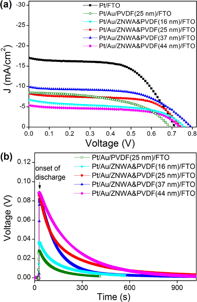
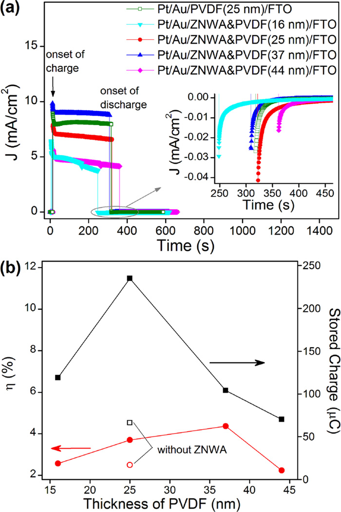
The pure DSSC shows the highest η in Fig. 3a (up to 7.32%). When the CE was modified by PVDF/ZNWA nanocomposites, η dropped to 2.23% – 4.36%. The dependence of η on the thickness of PVDF is shown in Fig. 4b, where the performances of the PSCs with 25- and 37-nm-thick PVDF are much greater than those of the others. PVDF either too thick or too thin could deteriorate the photovoltaic performance of such DSCs. The PSC with 44-nm-thick PVDF has the poorest photovoltaic performance, indicating that the reduced discontinuity in PVDF blocks the transport of electrons for photo-to-electric conversion. For comparison, a PSC with a CE of planar structure without ZNWA is also shown in Fig. 3a and Fig. 4b. The PSC with 25-nm-thick planar PVDF (without ZNWA) has a much lower η than that of the PSC with 25-nm-thick PVDF coating on ZNWA. It indicates that the introduced ZNWA helps to improve the transport of electrons for the photovoltaic process, presumably due to the formed discontinuities in the PVDF film.
Figure 3.
(a) J-V curves of PSCs. (b) Open-circuit voltage of PSCs as a function of discharging time.
Figure 4.
(a) Charging and discharging J-t curves of PSCs. The inset: discharge curves zoomed in. (b) Dependences of η and stored charge on the thickness of PVDF. The two separate data points indicate the results of the PSC with planar PVDF structure without ZNWA: hollow circle – η; hollow square – stored charge.
On the other hand, compared to the pure DSSC, PSCs with CEs modified by PVDF/ZNWA nanocomposites demonstrated energy storage capability, which is shown by the discharging photovoltage transient (V-t) curves in Fig. 3b. The PSCs with 25-, 37-, and 44-nm-thick PVDF have greater energy storage capabilities than the one with 16-nm-thick PVDF. 16 nm might be so thin that the area of discontinuities in PVDF could be large, causing severe recombination that reduces the energy capacity. The PSC with planar PVDF coating has a much lower effective surface area, thus a low capacity. When the discharging began, the voltage polarity of each PSC was reversed with respect to the photovoltage, indicating that the discharging voltage was from the capacitor section. The initial voltages of the three better V-t curves in Fig. 3b were almost the same, at nearly 90 mV.
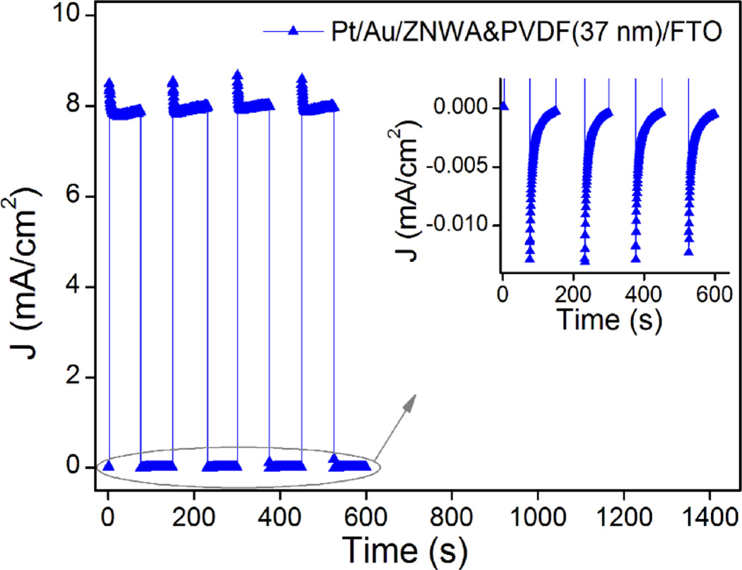
The charging-discharging photocurrent transient curves (J-t) were shown in Fig. 4a. For each curve, the photocurrent decreased to equilibrium values from the highest initial values in several tens of seconds under illumination, a typical charging nature of PSCs.[1–8] Similar to the results from the V-t curves, the direction of current was reversed when the discharging began. The stored charge for each PSC could be calculated from the integration of the discharging J-t curve, and the results depending on the thickness of PVDF are shown in Fig. 4b. Similar to the results of η, the PSCs with 25- and 37-nm-thick PVDF have greater charge capacities than the others. This result agrees well with the V-t results. The lower charge storage capability of the PSC with 44-nm-thick PVDF is due to its poor photovoltaic performance that limits the charging process. The poor charge capacity of the PSC with planar PVDF film further proves that ZNWA could greatly improve the effective surface area for charge storage. The PSC with 25-nm-thick PVDF possesses a charge storage density of 2.14 C g−1, much higher than 0.471 C g−1 of that with 37-nm-thick PVDF. SEM images of PVDF/ZNWA (Fig. 2) illustrate that the 25-nm-thick PVDF has a smoother surface on ZnO nanowires than that of 37-nm-thick PVDF. Both thickness and morphology could affect the static force between positive and negative charges on both sides of the PVDF film. Consequently, such confinement of Li+ could have significant effect on solar energy harvesting and conversion by changing the electron injection efficiency and conduction band edge of TiO2.[16] In addition, the cyclic test of the PVDF/ZNWA based PSC demonstrates good repeatability in photo-charging and discharging cycles, as shown in Fig. 5.
Figure 5.
Evolution with time of the photocurrent for a PVDF/ZNWA PSC under interrupted illuminations. The inset: discharge curves zoomed in.
The energy storage mechanism of PVDF/ZNWA nanocomposite has been described above and illustrated in Fig. 1b. We first excluded the contribution of the intercalation reaction of Li+ cations with ZnO for the charge storage by using a pristine PVDF film without ZNWA to modify the CE; an energy storage effect, though inferior to the cases with ZNWA, was observed as shown in Fig. 3 and Fig. 4. Furthermore, X-ray diffraction (XRD) spectra of PVDF film with and without ZNWA show that the presence of ZNWA shifts the mixed β phase peak at 20.04° of pristine PVDF film toward the left and down to 20.00°, corresponding to a lower β phase component, which indicates that the crystalline phase of PVDF in this work was predominantly α phase (Fig. S1).[17] Such result weakens the association of the energy storage capability with the ferroelectric effect resulting from β-phase PVDF. Thus we ascribe the energy storage of PVDF-contained PSCs to the dielectricity of PVDF. The Pt/Au layer on the surface of PVDF/ZNWA composite acts as a quasi-electrode for electrons to pass through. At the same time, electrons and Li+ cations accumulate on the surface of ZnO NWs and Pt/Au layer. The electrostatic capacity of a capacitor is inversely proportional to the thickness (d) of the dielectric: C ∝ ε/d, where ε is the dielectric constant. In this study, the density of the stored charge in the PSC with 25-nm-thick PVDF was higher than that in the PSC with 37-nm-thick PVDF, while the fully charged voltage of the two PSCs were almost the same. This implies that the thinner PVDF coating on ZNWA could provide higher charge capacity. The approximate stored energy density (E) could be calculated from the V-t curve. For the best-performance PSC with 25-nm-thick PVDF in this study, it was calculated to be E = 1.4 mWh kg−1, which is lower than the reported results of typical supercapacitors.[3] This is due to the lower discharging voltage, which is primarily caused by the recombination through the R section in Fig. 1b. In the future work, a photosensitive resistor will be introduced for this R, which could provide better electron path for the photovoltaic part under illumination and large resistance in dark for suppressing the leakage in the storage part. The performance of the PSC therefore could be greatly improved.
In conclusion, we demonstrated a simplex PSC with dual-functions of photocurrent output and energy storage, which can be realized concurrently. The charge storage was realized by modifying the CE with PVDF/ZNWA nanocomposites. The parameters of PVDF coating on inorganic nanomaterials such as thickness and morphology could affect both energy conversion and storage. The PSC with 25-nm-thick PVDF could provide steady photocurrent output and achieve a η of 3.70%, while part of the photo-generated charge is stored in CE with a charge density of 2.14 C g−1. This low-cost and easily fabricated dual-functional cell could have wide applications in electronics, such as sensor networks, which need to operate all day, continuously and unattended.
Experimental
ZNWAs were prepared on FTO glass (1.5 cm × 2 cm, TEC-15, MTI Co.) in a solution mixture (v:v = 1:1) of 0.25 m Zn(NO3)2 and 0.25 m hexamethylenetetramine at 92 °C for ~50 h.[18–20] 5 droplets of polyethylenimine (branched, low molecular weight, Aldrich) were added into 200 ml of ZnO growth solution to adjust the ratio of length/diameter of ZnO NWs. The ZnO seed layer was formed by prior spincoating of a mixture of 0.01 m zinc acetate/methanol solution and 0.03 m NaOH/MeOH solution (v:v = 4:1) onto the FTO substrate, followed by an oxidation process in air at 250 °C for 20 min. The PVDF/ZNWA nanocomposites with different PVDF thicknesses (16 nm, 25 nm, 37 nm, 44 nm) were prepared by dip-coating 5, 10, 20, 30 µL, respectively, of PVDF (Kynar 301F, Mw = 3.8 × 10⁵)/dimethylsulfoxide (DMSO, Aldrich) solution (1 g PVDF/100 g DMSO) onto the ZNWA, followed by drying at 90 °C in air for 30 min. For comparison, one sample with 25-nm-thick planar PVDF structure (without ZNWA) was also fabricated. A 20-nm-thick Au layer was first sputtered onto the surface of the PVDF/ZNWA nanocomposites by a Denton sputter coater Desk II. Then, a Pt layer was deposited onto the Au surface of the CE by an electrodeposition process in chloroplatinic acid (H2PtCl6; Aldrich) solution (0.5 m). Photoelectrodes were prepared by doctor-blade coating of a TiO2-containing viscous paste (Solaronix, 15 – 20 nm particles) onto the FTO substrate, followed by sintering at 500 °C for 1 h. After being cooled to 120 °C, the films were immersed into a 0.3 mM solution of N719 (Solaronix) in dry ethanol for 24 h. The photoelectrodes and CEs have the same active area of 0.23 cm2. TiO2 photoelectrode and the CE were separated by 50-µm spacers (Surlyn, Solaronix). The internal space of the cell was filled with a liquid electrolyte [0.05 m LiI, 0.03 m I2, 0.1 m guanidinium thiocyanate (GNCS), 1.0 m 1, 3-dimethylimidazolium iodide (DMII), 0.5 m 4-tertbutyl pyridine (TBP) in 3-methoxyproionitrile and acetonitrile (6:4)].
The morphology of ZNWA and PVDF/ZNWA surfaces were characterized by using an SEM (Zeiss LEO 1530). XRD spectra of PVDF films were measured by a Bruker/Siemens Hi-Star 2d X-ray Diffractometer with a monochromatic Cu K-alpha point source (0.8 mm). J-V performance was tested by using a Keithley 2400 source meter under AM 1.5G simulated sunlight (Newport 94022A equipped with a 150 W Xe lamp and AM 1.5G filter). The photovoltage and photocurrent transient curves (V-t, J-t) measurements were carried out by an Agilent 34411A 61/2 digital multimeter. The PSCs were illuminated under AM 1.5G for about 5 min before the light source was turned off for discharging measurements: through a 1 MΩ resistor for V-t; in short-circuit for J-t.
Supplementary Material
Acknowledgements
X. Zhang and X. Huang contributed equally to this work. This work was supported by the US National Institute of Health (Grant No. 1DP2OD008678-01). The authors thank Dr. Y. Liu for discussions and assistance. This research utilized NSF supported shared facilities at the University of Wisconsin. Supporting Information is available online from Wiley InterScience or from the author.
References
- 1.Miyasaka T, Murakami TN. Appl. Phys. Lett. 2004;85:3932. [Google Scholar]
- 2.Lo C, Li C, Jiang, H H. AIP Adv. 2011;1:042104. [Google Scholar]
- 3.Wee G, Salim T, Lam YM, Mhaisalkara SG, Srinivasan M. Energy Environ. Sci. 2011;4:413. [Google Scholar]
- 4.Chen H-W, Hsu C-Y, Chen J-G, Lee K-M, Wang C-C, Huang K-C, Ho K-C. J. Power Sources. 2010;195:6225. [Google Scholar]
- 5.Murakami TN, Kawashima N, Miyasaka T. Chem. Commun. 2005;26:3346. doi: 10.1039/b503122b. [DOI] [PubMed] [Google Scholar]
- 6.Guo W, Xue X, Wang S, Lin C, Wang Z. Nano Lett. 2012;12:2520. doi: 10.1021/nl3007159. [DOI] [PubMed] [Google Scholar]
- 7.Chen T, Qiu L, Yang Z, Cai Z, Ren J, Li H, Lin H, Sun X, Peng H. Angew. Chem. Int. Ed. 2012;51:11977. doi: 10.1002/anie.201207023. [DOI] [PubMed] [Google Scholar]
- 8.Song T, Sun B. ChemSusChem. 2013;6:408. doi: 10.1002/cssc.201200889. [DOI] [PubMed] [Google Scholar]
- 9.Grätzel M, Janssen RAJ, Mitzi DB, Sargent EH. Nature. 2012;488:304. doi: 10.1038/nature11476. [DOI] [PubMed] [Google Scholar]
- 10.Hardin BE, Snaith HJ, McGehee MD. Nat. Photonics. 2012;6:162. [Google Scholar]
- 11.Yella A, Lee HW, Tsao HN, Yi CY, Chandiran AK, Nazeeruddin MdK, Diau EWG, Yeh CY, Zakeeruddin SM, Grätzel M. Science. 2011;334:629. doi: 10.1126/science.1209688. [DOI] [PubMed] [Google Scholar]
- 12.Ding I-K, Zhu J, Cai W, Moon S-J, Cai N, Wang P, Zakeeruddin SM, Grätzel M, Brongersma ML, Cui Y, McGehee MD. Adv. Energy Mater. 2011;1:52. [Google Scholar]
- 13.Morales-Acevedo A. Appl. Phys. Lett. 2005;86:196101. [Google Scholar]
- 14.Wang G, Deng Y, Guo L. Adv. Funct. Mater. 2008;18:2584. [Google Scholar]
- 15.Gregorio R, Jr, Borges DS. Polymer. 2008;49:4009. [Google Scholar]
- 16.Jennings JR, Wang Q. J. Phys. Chem. C. 2010;114:1715. [Google Scholar]
- 17.Ma W, Zhang J, Chen S, Wang X. J. Macromol. Sci. B. 2008;47:434. [Google Scholar]
- 18.Zhang Q, Dandeneau CS, Zhou X, Cao G. Adv. Mater. 2009;21:4087. [Google Scholar]
- 19.Law M, Greene LE, Johnson JC, Saykally R, Yang P. Nat. Mater. 2005;4:455. doi: 10.1038/nmat1387. [DOI] [PubMed] [Google Scholar]
- 20.Pacholski C, Kornowski A, Weller H. Angew. Chem. 2002;41:1188. doi: 10.1002/1521-3773(20020402)41:7<1188::aid-anie1188>3.0.co;2-5. [DOI] [PubMed] [Google Scholar]
Associated Data
This section collects any data citations, data availability statements, or supplementary materials included in this article.


