

Abstract
Microfabricated devices designed to provide phase contrast in the transmission electron microscope must be free of phase distortions caused by unexpected electrostatic effects. We find that such phase distortions occur even when a device is heated to 300 °C during use in order to avoid the formation of polymerized, carbonaceous contamination. Remaining factors that could cause unwanted phase distortions include patchy variations in the work function of a clean metal surface, radiation-induced formation of a localized oxide layer, and creation of a contact potential between an irradiated area and the surround due to radiation-induced structural changes. We show that coating a microfabricated device with evaporated carbon apparently eliminates the problem of patchy variation in the work function. Furthermore, we show that a carbon-coated titanium device is superior to a carbon-coated gold device, with respect to radiation-induced electrostatic effects. A carbon-coated, hybrid double-sideband/single-sideband aperture is used to record in-focus, cryo-EM images of monolayer crystals of streptavidin. Images showing no systematic phase error due to charging are achievable under conditions of low-dose data collection. The contrast in such in-focus images is sufficient that one can readily see individual streptavidin tetramer molecules. Nevertheless, these carbon-coated devices perform well for only a limited length of time, and the cause of failure is not yet understood.
Keywords: Phase contrast, charging, cryo-EM, phase plate
1. INTRODUCTION
Numerous designs have been proposed for microfabricated devices that could produce in-focus contrast for weak-phase objects in the transmission electron microscope (TEM). A miniature, planar-electrode einzel lens, first proposed by Boersch [1] for use as a phase plate, has shown great potential in recent work [2–4]. Progress is also being made on an analogous magnetic phase-plate design [5]. Other designs for electrostatic phase plates include a shielded drift tube [6] and a device that produces a strongly localized electrostatic potential at the tip of a microfabricated bar (referred to as the Zach phase plate) [7]. Devices have been demonstrated that apply a phase shift of 180° to one half plane in Fourier space relative to the other, using either a thin carbon film [8] or a narrow magnetic bar [9]. Similarly, a microfabricated device that completely blocks a half plane in Fourier space, but only at low spatial frequencies, has also been proposed. This type of device is described as being a hybrid double-sideband/single-sideband (DSB/SSB) aperture [10]. Finally, a thin carbon film with a hole at the center, again first proposed by Boersch [1], has been developed to the point that excellent results can be obtained with unstained biological specimens [11–13]. This design, in spite of its limitations [14, 15], is currently the device that gives the best performance.
In work done to date, all such devices suffer from variable, often unacceptable levels of electrostatic charging [10, 14, 15]. Electrostatic charging causes unwanted distortions in the phase of the scattered wave, and these phase distortions produce corresponding distortions in the contrast transfer function (CTF). In some of the worst examples of charging, the CTF may show azimuthal distortions that cannot be corrected by the image stigmator, or – more subtly – the radial dependence of a circularly symmetrical CTF may not fit the expected dependence on spherical aberration and defocus [10, 15].
We now report that coating a hybrid DSB/SSB aperture with evaporated carbon is effective in producing charging-free devices. We believe that the layer of evaporated carbon serves two, important functions. Coating the surface of a device with an electrically conducting, amorphous material produces a surface with a uniform work function, thus ensuring that the isopotential surface conforms to the shape of the microfabricated device. In addition, an evaporated carbon film, unlike most other materials that might be considered, is not expected to form an oxide that is thicker than an atomic monolayer. It is also effective to “wrap” a thin carbon-film phase plate with a final coating of evaporated carbon, but in this case the intent is to cover up surface contamination that might be deposited in earlier stages of fabrication [14, 16].
We have found that fabricating apertures from titanium gives results that are superior to fabricating them from gold. Although carbon-coated gold devices remain charging-free as the edge of the aperture is brought close to the unscattered beam, an unwanted patch potential quickly forms if the edge of the aperture is actually touched by the unscattered beam. When titanium is used, we still observe such a patch potential, but its magnitude is much smaller than when gold is used.
In addition, we find that heating a carbon-coated device well above 300 °C improves the extent to which it remains free of charging artifacts. We believe that high temperatures may serve to repair (anneal) radiation damage that occurs in the irradiated amorphous carbon coating, as it is known that annealing of radiation damage occurs in irradiated graphite at a temperature above 200 °C [17, 18]. Nevertheless, the apertures become more sensitive to charging as they get older, and we find that it is impractical to use them for longer than a week to 10 days after carbon coating.
Finally, using a carbon-coated titanium device, heated to ~400 ° C, we have obtained in-focus cryo-EM images of monolayer crystals of streptavidin. This specimen was chosen to demonstrate the high level of contrast produced at low spatial frequencies, as well as to confirm that phase distortions due to charging remain negligible under low-dose imaging conditions.
2. MATERIALS AND METHODS
2.1 Fabrication of hybrid DSB/SSB apertures
2.1.1 Apertures are milled from thin-foil stock with a focused ion beam (FIB)
Apertures with the desired size and shape were cut into thin-foil substrates, using the gallium-ion beam in a Zeiss XB 1540 cross-beam tool. The hybrid DSB/SSB apertures can be described as a large open circle with an opaque, smaller half-circle at the center, which is necessarily supported by a beam extending from the outer rim of the large circle. Because of its distinctive profile, this type of aperture has been referred to as a “tulip” aperture [10]. In the example shown in Figure S1, the straight edge of the opaque half circle is off set by equal (but opposite) amounts on either side of the center, thus producing a notch (step) at the center. In the current experiments the diameter of the aperture was >400 μm, the diameter of the opaque half circle was ~70 μm. The height of the notch was ~1.5 μm. The apertures were created by milling a trench around the perimeter of what became the open area. When the trench was cut all the way through the foil, the central piece dropped out but usually adhered to one edge of the hole. This adhering piece was easily removed by blowing compressed nitrogen over the surface of the foil. As time allowed, we have milled up to 5 apertures on one strip.
Experimental apertures were fabricated from 5 μm-thick gold foil (ESPI Metals, Inc.), 5 μm-thick titanium foil (Goodfellow), and 5 μm-thick membranes of boron–doped silicon supported on a silicon chip, fabricated from an SOI wafer (Ultrasil Corp.). Numerous surface-cleaning protocols were tested for each type of foil, until a satisfactory recipe was developed. For gold apertures, we first sonicated the as-received foil with Alconox detergent in water, then rinsed in acetone and deionized water, then further cleaned with 20% nitric acid in water, again sonicated in deionized water, and finally rinsed with isopropyl alcohol. The as-received titanium foil was sonicated with acetone and then rinsed by sonication with deionized water. For silicon apertures the final step was to remove the native oxide as completely as possible by dipping in a 10% solution of HF in water and rinsing with deionized water.
2.1.2 Conformal coating of apertures with evaporated carbon
Conformal coating was achieved by evaporating carbon in two steps, first onto the top surface of the device and then onto the bottom surface. The point source of the carbon arc was placed at an angle of ~45° to the plane of the aperture, and the device was rotated in the plane of the aperture during evaporation (see Figure S2 for further details). The aperture was placed at a distance of ~8–10 cm from the carbon arc. Carbon was evaporated in a single step (for each side of the device), using sufficient power in the arc to evaporate the thin tip over a matter of just one or a few seconds. The resulting thickness of carbon was estimated to be between 20 nm and 30 nm, as judged from the darkness of the carbon deposited on a piece of filter paper that was placed next to the device. Carbon evaporation was performed in an oil-pumped Denton DV-502 evaporator, at a vacuum in the range 4×10⁻⁶ to 8×10⁻⁶ torr.
2.2 Electron microscopy using the hybrid DSB/SSB aperture
2.2.1. Key features of the microscope and the phase-contrast aperture holder
Experiments were performed with an FEI Titan 80–300 electron microscope that was modified by the vendor to provide a 6-fold magnification of the electron diffraction pattern at the plane of the phase-contrast aperture. This modification involved the addition of a lens (together with accompanying beam deflectors and stigmators) in the section of the column that would otherwise be used for an aberration corrector. When this additional lens, referred to as the transfer lens (X lens), is “on”, the excitation of the objective lens is increased slightly and the Lorentz lens (objective minilens) is turned on. These modifications increase both the spherical and chromatic aberration of the final image. The net aberration constants were calculated to be Cs = 4.6 mm and Cc = 7.2 mm, and they were measured to be Cs = 4.8 mm and Cc = 7.2 mm. All images shown here were recorded at 300 keV using parallel illumination conditions (illumination half-angle estimated to be less than 20 μradian). The CTF at Scherzer defocus has a first zero above 1/(0.3 nm), and the effects of both the temporal- and spatial-coherence envelope functions are small out to that resolution.
Four ports are provided at points around the column, in the plane where the transfer lens system produces the magnified diffraction pattern. One of these ports is used as a vacuum feed-through for insertion of a home-built aperture rod, the tip of which can be either heated or cooled. Once the aperture is inserted into the microscope column, its position is controlled with a precision of ~20 nm, using linear piezo stages (Physik Instrumente) that provide a travel of 50 mm parallel to the axis of the rod and 8 mm perpendicular to the axis. The aperture rod is withdrawn into an airlock whenever apertures are to be exchanged. Further details regarding the aperture rod and the airlock are presented in the Supporting Material.
Although experiments were performed at aperture-temperatures as low as −80° C and as high as 450° C, the results presented here were all obtained at an aperture temperature between 300 and 410 °C. Starting from room temperature, the aperture reaches thermal equilibrium within ~1.5 hour. The tolerance regarding drift and vibration is much greater for the position of the aperture, of course, than it would be for a specimen stage.
2.2.2. Use of Thon rings to evaluate charging
A variety of different thin-carbon-film specimens was used, including commercially purchased holey-carbon films bearing particles of graphitized carbon; gold-shadowed carbon replicas of an optical diffraction grating; and various home-made carbon or Pt-carbon thin films. An FEI Eagle CCD camera was used for the majority of the experiments in which we evaluated charging of various apertures, (as well as for the initial cryo-EM work, described in section 2.2.3, below). During the final stages of this work, however, the Eagle camera was replaced with a Gatan K2 Summit camera.
Images recorded with the unscattered beam in the center of the largest open area of the tulip aperture served as the initial point of reference, nominally free of distortions due to charging. The performance of the aperture was then judged while centering the aperture, thus bringing the straight edge of the opaque half circle within one micrometer or less of the focused, unscattered beam in the electron diffraction pattern. The power spectra of these images, displayed in real time, were used to evaluate the extent to which charging of a given aperture did, or did not, produce distortions in the contrast transfer function, i.e. in the Thon rings.
2.2.3. Cryo-EM data collection and analysis
Monolayer crystals of streptavidin (Sigma-Aldrich) were used to characterize the effectiveness of hybrid DSB/SSB apertures in terms of producing interpretable contrast for in-focus images of weak phase objects. Crystals were grown as described by [19, 20], picked up by Langmuir-Shafer transfer using C-flat EM grids, and frozen with the use of an FEI Vitrobot. Images of untilted specimens exhibit cmm symmetry, with unit cell dimensions estimated to be a = 8.05 nm, b = 8.16 nm.
Cryo-EM images were recorded with the use of FEI Low Dose software. During the Search step of a low-dose cycle, the notched edge of the “tulip” aperture was retracted to a position far enough away from the unscattered beam that the opaque half circle did not obscure the field of view. During the Focus step of a low-dose cycle, the aperture was left in the same (retracted) position, so that it would not be unnecessarily exposed to electrons scattered at small angles. During the Expose step of a low-dose cycle, the aperture was returned to its well centered position (with the beam blanked) before an image was recorded. Following this the aperture was again retracted in preparation of another Search, Focus, and Expose cycle.
Streptavidin-monolayer crystals were chosen as a test specimen because the relatively strong SNR for structure factors at the reciprocal lattice points makes it practical to compare the phases from two successive images of the same area. Data were recorded as pairs of images, the first of which was taken close to Scherzer focus with the tulip aperture, and the second of which was taken, without the aperture, at about 3.7 μm under focus. Data analysis was limited to a highest resolution of 1.3 nm, corresponding to the cutoff frequency of the opaque half circle of the tulip aperture.
The phases of the Fourier transform of the first image (in a pair) were first corrected for the systematic phase error [10] of (π/2 – γ(s)), where γ(s) was modeled by a quadratic phase shift that reached a value of 30° at the radius of the opaque half circle. An inverse Fourier transform then provided a corrected single-sideband image. The software 2dx [21, 22] was then used to find the symmetry origin for which the Fourier transform best satisfied the known cmm symmetry of images of untilted specimens. Similarly, the phases of the Fourier transform of the second image (in a pair) were corrected for changes in sign of the CTF, and an inverse Fourier transform provided a corrected double-sideband image. Once again, 2dx was used to find the same symmetry origin as was used for the corrected single-sideband image. Image unbending and extraction of structure-factor phases was also performed with 2dx.
3. RESULTS
3.1. Carbon-coated titanium apertures can exhibit robust, charging-free behavior during use
3.1.1. Computed power spectra can show no apparent distortions as the edge of an aperture approaches the unscattered electron beam
The power spectrum of an image of a thin carbon-film specimen does not show any obvious change when a successfully fabricated, carbon-coated titanium aperture is moved close to the unscattered beam in the electron diffraction pattern. The aperture must be free of particulate contamination for this to be the case, however. Indeed, failure of such an aperture to be free of charging effects at this stage of the evaluation has proven to be a sensitive indicator that unwanted particles have adsorbed to an aperture, as can subsequently be confirmed by inspection in an SEM. In addition, some apertures that we have made appear to have been free from particulate contamination, and still they caused astigmatism or exhibited other forms of charging, the amount of which varied from one aperture to another on the same strip. We suspect that this variability may be due to variations in the thickness of the oxide layer on the as-received titanium foil.
Figure 1 shows an example of the stability of the power spectrum of images of a carbon film, as the edge of charging-free aperture is brought close to the unscattered beam in the electron diffraction pattern, and then it is retracted again. The focus and astigmatism of the image were not adjusted at any time in this series, yet – as desired – the Thon rings in Figure 1C remain circular and the radius of each ring remains the same as it was in Figure 1A, after the edge of the aperture is withdrawn. No unwanted glow, flame, or bubble of anomalous contrast transfer has been introduced at spatial frequencies close to the edge of the aperture, even though it was brought very close to the unscattered electron beam in the electron diffraction pattern.
Figure 1.
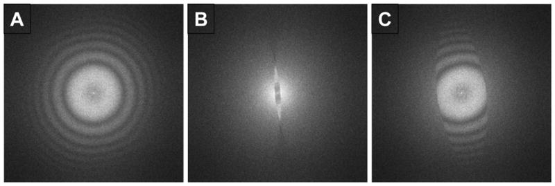
Example of the robust, charging-free performance of a successfully made, carbon-coated titanium aperture. (A) Fourier transform of an image recorded with the edge of the aperture far away from the unscattered beam in the electron diffraction pattern. The Thon rings seen here serve as a point of reference for the subsequent panels. (B) Fourier transform of an image recorded when the edge of the aperture is very close to the unscattered beam in the electron diffraction pattern. The purpose this panel is to show the high contrast that is present at low spatial frequency in the single-sideband portion of the Fourier spectrum (i.e. behind the edge of the aperture) but not in the double-sideband portion. The fact that there is no “glow” of anomalous contrast at the edge of the aperture, in the double-sideband area, confirms that there is no (unwanted) phase shift due to charging of the aperture, even though the unscattered electron beam is very close to the edge. (C) Fourier transform of an image recorded with the edge of the aperture retracted away from the unscattered beam. This panel confirms that the Thon rings are not distorted by the presence of the aperture, not even at spatial frequencies close to the edge of the aperture.
Importantly, when the edge of the aperture is close to the unscattered beam, as it is in Figure 1B, the power at low spatial frequencies is very strong within the single-sideband portion of the spectrum (corresponding to the opaque portion of the aperture), while the power in the double-sideband portion does not change. When, on the other hand, the edge of an aperture charges, phase shifts are produced by the electrostatic potential that is introduced into the double-sideband portion of Fourier space, and these unwanted phase shifts cause obvious changes in the power spectra. An extreme example illustrating this latter behavior (for a carbon-coated gold aperture) is shown in section 3.2.
3.1.2. High contrast is produced for in-focus images of streptavidin crystals
Figure 2A shows a representative example of the images of streptavidin monolayer crystals that are obtained with the tulip aperture. Figure 2B shows the image of the same crystal shown in Figure 2A, at the same setting of focus, but with the aperture retracted. The streptavidin lattice is no longer visible in this nearly in-focus, double-sideband image. To establish that the absence of visible structure in this case is not due simply to radiation damage, a second double-sideband image was taken of the same area, but this time with an under-focus value of 3.7 μm. As is shown in Figure 2C, the streptavidin lattice is still well preserved at low resolution, although we are aware that the higher-resolution features will have been destroyed before this third image was recorded. Each image was recorded with an electron exposure of ~1500 electron/nm2.
Figure 2.
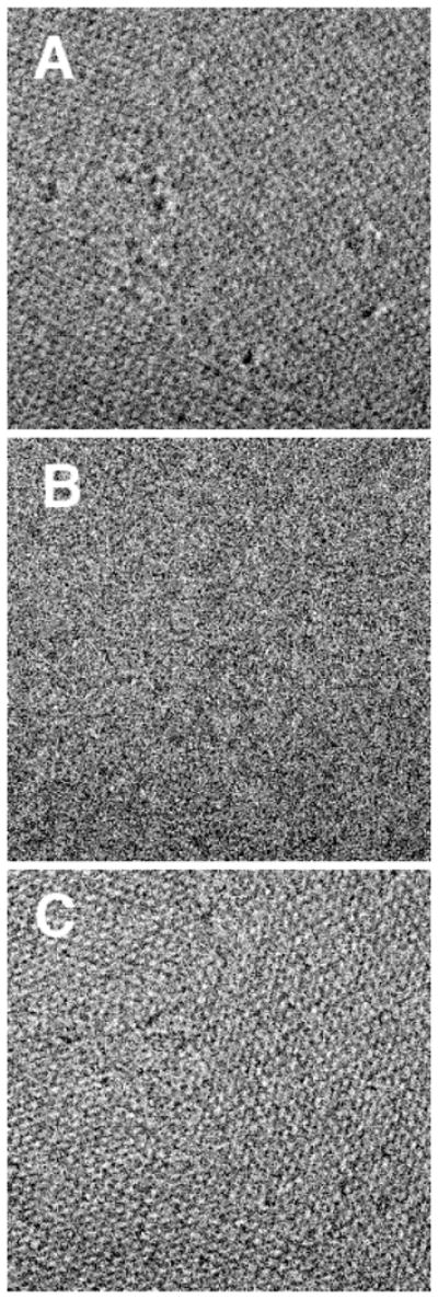
Three successive images recorded at the same area of a streptavidin monolayer crystal, using an electron exposure of approximately 1500 electrons/nm2 for each image. This series illustrates the fact that in-focus images of weak phase objects have high contrast when taken with the tulip aperture. While the second and third image in the series must suffer successively greater degrees of radiation damage, the effects of this damage are not expected to be apparent at the low resolution of features that can be seen by eye. The unit-cell dimensions of the streptavidin crystal are estimated to be a = 8.05 nm, b = 8.16 nm. (A) Image taken close to focus, with a well-centered tulip aperture. (B) Image taken without changing the focus value, but with the tulip aperture retracted. (C) Image again taken with the tulip aperture retracted, but after under-focusing the image by ~3.7 μm.
The streptavidin specimens proved to have a further advantage in that individual streptavidin tetramers (MW ~55 kDa) are randomly distributed in the areas between separate 2-D crystals. Images of these particles thus provide a good demonstration of the contrast produced in in-focus images when using the hybrid DSB/SSB aperture.
3.1.3. A “CTF-like correction” is still required when using a hybrid DSB/SSB aperture
The Fourier components of a single-sideband image are expected to have only half of the amplitude of a Zernike phase-contrast image, and in addition the phases of the Fourier components are expected to have a systematic error of (π – γ(s)) [10], where γ(s) is the familiar wave aberration due to spherical aberration and defocus. One must thus make systematic corrections for these effects in order to recover an image intensity that is proportional to a projection of the structure of the specimen. When images are recorded close to focus, γ(s) is close to zero at low to intermediate frequencies, but it is still important to correct for the systematic phase error of π/2. One may also want to boost the amplitudes by a factor of 2, but that correction is less important.
A very simple (but incomplete) restoration algorithm is to multiply one half-plane of the Fourier transform of an image by exp(iπ/2) = i at the spatial frequencies that were imaged in the single-sideband mode. Furthermore, the relatively small phase error associated with γ(s) is modeled by a parabola that reaches a maximum value of 30° at a spatial frequency corresponding to the radius of the opaque half circle, assuming that the image was recorded with a defocus value such that sin γ(s) = 0.5 at this spatial frequency. The complementary half plane is then generated by imposing Friedel symmetry. Figure 3 shows an example of an image (A) as-recorded and (B) after applying this simple restoration. The “optical shadowing” effect, characteristic of single-sideband images, is noticeably reduced in (B), and one can now more easily distinguish single streptavidin tetramers in the non-crystalline area between crystalline domains, even before restoration. In addition, various types of defect, even some too small to be seen in the raw image, become apparent after image restoration. Other, more complete restoration algorithms are possible, of course, but these require that one have an accurate estimate of γ(s) for each image.
Figure 3.
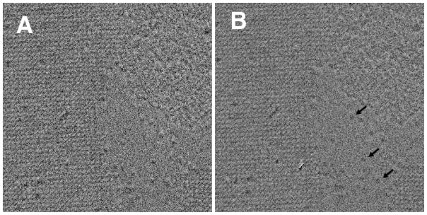
Illustration of the effectiveness of image restoration. An image was selected that contains a streptavidin monolayer crystal on the left and a disordered monolayer of streptavidin molecules clustered at the top right. A nearly empty region of the lipid monolayer is present at the center and lower right of this image. Individual streptavidin tetramers (Mr = 55 k), which are present within this sparsely populated area, can be seen in both the raw and the restored versions of the image. The unit-cell dimensions of the streptavidin crystal are estimated to be a = 8.05 nm, b = 8.16 nm. (A) The “raw” image, showing the “optical shadowing” effect that is present before restoration. (B) Restored image with arrows identify three examples of streptavidin tetramers. This image was produced by applying a systematic correction of 90 degrees to the phases for all spatial frequencies within the single-sideband region of the Fourier transform of the raw image. A quadratic phase-correction, rising to a value of 30 degrees at a spatial frequency of 1/(1.3 nm), was also applied as part of the restoration procedure.
3.1.4. Diffraction spots in the Fourier transforms of images of streptavidin crystals show no systematic phase error in the single-sideband area of the Fourier transform
Figure 4C documents that there does not appear to be a systematic (global) difference in the structure-factor phases for the SSB images compared to the DSB images, as there would be if there was significant charging of the aperture. We limited this comparison to spatial frequencies within the single-sideband region. In addition, we include only reflections where the IQ in both images was 5 or smaller, ensuring that the phase error due to limited signal-to-noise of the measurements would not exceed 30° (see Table 10.1 in Glaeser et al. [23]). Numerical values of the structure-factor phases are listed in Table 1 for three such comparisons of SSB and DSB images, as well as one comparison for two successive DSB images.
Figure 4.

Comparison of the Fourier transforms of images of a streptavidin monolayer crystal recorded with or without the tulip aperture, respectively. An electron exposure of ~1500 electrons/nm2 was used in each case. First an in-focus image was recorded using the tulip aperture, and then a second image was recorded of the same area without the tulip aperture, under-focused by ~3.7 μm. (A) The Fourier transform of the first image, with the insert showing an enlargement of the boxed area. (B) The Fourier transform of the second image, with the insert again showing an enlargement of the boxed area. (C) Graphical representation of the structure-factor phases. The length of a vector represents the IQ of the reflection (the longer the arrow, the lower the IQ value), and the direction represents its phase. The values of IQ and phase shown in this figure correspond to the values shown for SSB2 and DSB2 in Table 1. The similar direction of vectors shows that there does not appear to be a systematic phase error in the single-sideband portion of the Fourier spectrum.
Table 1.
Comparison of structure-factor phases of monolayer crystals of streptavidin for three examples of single-sideband (SSB), double-sideband (DSB) image pairs, and for one example of a DSB, DSB image pair. The image pairs were recorded with an electron exposure of ~1500 electron/nm2 for each image, and appropriate image-restoration corrections were applied, as described in the text. Diffraction spots are listed by increasing resolution (right-hand column) and the corresponding Miller indexes are shown in the two columns on the left. For each image pair, structure-factor phases are listed along with the IQ of the reflection. Entries are shown only if the IQ value is 5 or lower for both images in a pair.
| H | K | Phase | IQ | Phase | IQ | Phase | IQ | Phase | IQ | Res. (Å) | ||||||||
|---|---|---|---|---|---|---|---|---|---|---|---|---|---|---|---|---|---|---|
| SSB1 | DSB1 | SSB1 | DSB1 | SSB2 | DSB2 | SSB2 | DSB2 | SSB3 | DSB3 | SSB3 | DSB3 | DSB4 | DSB5 | DSB4 | DSB5 | |||
| 1 | −1 | −176 | −178 | 1 | 1 | −176 | −176 | 1 | 1 | −177 | 177 | 1 | 1 | 178 | 180 | 1 | 1 | 58.2 |
| 1 | 1 | −179 | 178 | 1 | 1 | −170 | −179 | 1 | 1 | 178 | −179 | 1 | 1 | −174 | −180 | 1 | 1 | 58.2 |
| 0 | 2 | 180 | −178 | 1 | 1 | −161 | 178 | 1 | 1 | 178 | −176 | 2 | 1 | −175 | 178 | 1 | 1 | 41.2 |
| 2 | 0 | −5 | 0 | 1 | 1 | 8 | 6 | 1 | 1 | 16 | 0 | 1 | 1 | 5 | 0 | 1 | 1 | 41.2 |
| 2 | −2 | 0 | 1 | 1 | 2 | 10 | 12 | 1 | 2 | 29.1 | ||||||||
| 2 | 2 | 33 | 72 | 2 | 3 | −3 | 2 | 1 | 2 | 29.1 | ||||||||
| 1 | −3 | −14 | −15 | 1 | 2 | 3 | 4 | 1 | 3 | −4 | −7 | 1 | 1 | 26.0 | ||||
| 1 | 3 | 19 | 16 | 2 | 4 | −12 | 16 | 2 | 5 | −24 | −15 | 2 | 2 | 26.0 | ||||
| 3 | −1 | −3 | 0 | 1 | 2 | 7 | 31 | 1 | 2 | 1 | −1 | 1 | 1 | 26.0 | ||||
| 3 | 1 | −15 | −8 | 2 | 2 | 17 | −30 | 1 | 3 | 2 | −6 | 1 | 2 | 26.0 | ||||
| 0 | 4 | 17 | −5 | 2 | 2 | 68 | −12 | 4 | 2 | −14 | −11 | 2 | 3 | −8 | −29 | 4 | 5 | 20.6 |
| 4 | 0 | 163 | 169 | 2 | 3 | −178 | 180 | 3 | 2 | −133 | 15 | 4 | 5 | 20.6 | ||||
| 3 | −3 | 10 | −50 | 4 | 5 | 11 | 25 | 3 | 2 | 19.4 | ||||||||
| 2 | −4 | −61 | 22 | 2 | 3 | −18 | 1 | 3 | 2 | −10 | −12 | 1 | 2 | 18.4 | ||||
| 2 | 4 | −21 | −1 | 4 | 4 | −32 | −17 | 3 | 5 | −16 | 15 | 2 | 3 | 18.4 | ||||
| 4 | −2 | 177 | −177 | 1 | 1 | 166 | −172 | 1 | 1 | 144 | 180 | 1 | 1 | 176 | 179 | 1 | 1 | 18.4 |
| 4 | 2 | 160 | −177 | 1 | 1 | −176 | 179 | 1 | 2 | −159 | −177 | 1 | 2 | 178 | 179 | 1 | 1 | 18.4 |
| 5 | −1 | −55 | −23 | 3 | 5 | 16.1 | ||||||||||||
| 5 | 1 | −25 | −23 | 2 | 5 | 4 | −2 | 2 | 3 | −8 | 16 | 2 | 4 | 16.1 | ||||
| 4 | −4 | 8 | 2 | 2 | 1 | 0 | −15 | 2 | 2 | −3 | 11 | 2 | 2 | 14.5 | ||||
| 4 | 4 | 0 | 3 | 2 | 2 | 0 | −11 | 2 | 1 | 3 | 2 | 2 | 2 | −19 | 0 | 2 | 3 | 14.5 |
| 3 | −5 | 31 | −2 | 2 | 1 | −2 | −1 | 2 | 1 | −1 | −4 | 3 | 2 | 1 | −13 | 2 | 1 | 14.1 |
| 3 | 5 | −10 | −29 | 1 | 2 | 0 | 0 | 2 | 1 | −1 | −5 | 2 | 2 | 2 | −25 | 2 | 4 | 14.1 |
| 5 | −3 | 153 | 171 | 3 | 4 | −162 | −146 | 4 | 3 | 134 | 96 | 4 | 4 | −161 | −154 | 3 | 4 | 14.1 |
| 5 | 3 | 171 | −139 | 4 | 5 | 14.1 | ||||||||||||
| 6 | 0 | −23 | 30 | 5 | 3 | −1 | 6 | 2 | 2 | 13.7 | ||||||||
| 6 | −2 | −83 | −15 | 3 | 2 | 13.0 | ||||||||||||
Although there does not appear to be a systematic (i.e. charging) effect, there nevertheless are a few reflections where there is a larger than expected discrepancy in phase between the first (i.e. SSB) and second (i.e. DSB) image. We believe that a change in specimen tilt-angle, due to beam-induced movement [24], could be the main factor contributing to this discrepancy. Figures 4A and 4B show that there are, indeed, some significant increases in the amplitudes of the second Fourier transform, contrary to the decreases expected from radiation damage. This demonstrates that the continuous structure factor must have been sampled at different points on the reciprocal lattice line during the first and second image, i.e. that the average tilt-angle of the specimen is, indeed, significantly different in the first and second image. We note that radiation-induced changes in tilt angle have also been found to occur between the first and second images for cryo-EM specimens of virus particles [25].
3.1.5. A low-dose (minimal exposure) protocol is still needed to keep the aperture free of charging when recording many successive images
We find that the carbon-coated, heated titanium aperture remains free of charging during at least 2 or 3 days of low-dose data collection. On the other hand, such devices acquire an unacceptable level of charging over an hour or less if a low-dose protocol is not used. We have also observed (but not quantified the dependence on time and temperature) that acceptable performance is slowly restored if the “damaged” aperture is no longer exposed to scattered electrons. We note that the thermal annealing of radiation damage, mentioned previously, may be kinetically slow and depend upon the rate of heating [18]. As is more fully explained in section 4.2, we thus believe that electrostatic charging may be due to a structural change in the carbon itself, caused by radiation damage, and that heating promotes a recovery of the structural properties. We further hypothesize that the use of a low-dose protocol not only limits the amount of “damage” that is done during the Exposure phase of a cycle, but it also allows time, during the Search and Focus phase of a cycle, to partially recover from the limited “damage” that does occur during the Expose phase.
3.1.6. Carbon-coated apertures become more sensitive with time, even when not exposed to electron irradiation
The “aging” of thin-carbon film phase plates has been noted previously [14]. A similar “aging” effect is also seen for our carbon-coated titanium apertures. While we have observed the charging-free performance described above for the first few days, it is our experience that about a week or ten days later the tulip aperture becomes much more sensitive to the edge being placed close to the unscattered electron beam. We have even seen this sensitivity appear suddenly from one day to the next. In work performed to date, the aperture has been held in the airlock between experiments at a vacuum in the 10−7 torr range and a temperature of 200 °C. Systematic studies of the aging phenomenon are very time consuming, and thus we have not yet determined whether aging is affected by the temperature at which the aperture is held when not in use.
3.2. The behavior of carbon-coated gold and carbon-coated silicon apertures is less robust
As was the case for a titanium aperture, the power spectrum of an image of a thin carbon film again does not show any obvious change when the edge of a carbon-coated gold aperture is brought close to the unscattered beam in the electron diffraction pattern. The results shown in Figure 5 illustrate the fact that the edge of the aperture can again be brought very close to the unscattered electron beam without introducing astigmatism or a change in the radius of the Thon rings. There is a suggestion, however, which we have not pursued quantitatively, that the power at low spatial frequencies within the double-sideband region is reduced somewhat relative to what it is when the edge of the aperture is farther from the unscattered beam.
Figure 5.
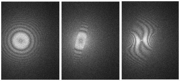
Example showing that a carbon-coated gold aperture does not become charged as the edge of the aperture is first brought close to the unscattered electron beam in the electron diffraction pattern. Nevertheless, a strongly charged patch is created if the unscattered electron beam is allowed to touch the edge. The left-hand panel shows the Thon rings when the unscattered electron beam is in the open area of the aperture, far from any edge. The middle panel shows that the radius of the Thon rings does not change as the edge of the aperture is brought close to the unscattered electron beam. The right hand panel, however, shows that the Thon rings are severely distorted by the patch potential created after the unscattered electron beam was allowed to briefly touch the edge.
On the other hand, the disappointing feature of carbon-coated gold apertures is the fact that they do not tolerate being hit directly by the unscattered electron beam. As Figure 5 shows, severe charging of the aperture occurs after the unscattered beam hits the edge for as short a time as 10 s. In this case a localized, strong patch of charging appears at the point where the electron beam had hit the aperture. The resulting phase shifts produce multiple oscillations of the amplitude of the Fourier transform, which are centered at the point where the electron beam touched the aperture rather than about the origin of the Fourier transform. Because the performance of the gold aperture was not as robust as that of the titanium aperture, we did not make a further, quantitative comparison of the experimental CTF relative to the theoretical curve, nor did we perform experiments with streptavidin monolayer crystals to characterize the phase errors that would occur within the single-sideband area of the aperture.
In the case of the carbon-coated silicon aperture, distortion of the Thon rings became apparent even when the edge of the aperture was 20 micrometers away from the unscattered electron beam, and these distortions became progressively worse as the edge was brought even closer. Since the carbon-coated silicon aperture clearly would not be useful, even under low-dose data conditions, we did not characterize its performance further. In addition, we have not explored why there is such a large difference for carbon-coated Si, Au, and Ti devices, but it is possible that this may have something to do with the interface between the material of the aperture and the evaporated-carbon coating.
4. DISCUSSION
4.1. Charging effects can be grouped into three conceptually distinct categories
4.1.1. The first such category consists of “particulate contamination”
We include in this category, among other things, (1) airborne particles that adsorb to a device during handling and (2) insulating particles or materials that are embedded into the device during fabrication of the foil, and which are exposed at the surface of the final device. Spots of polymerized, carbon-rich contamination that are formed when a device is hit by a highly focused electron beam can also be included in this category because of the insulating nature of such contamination. In all such cases, the distortions of the CTF appear to originate from, or to be centered on, the insulating “particle”. One can suspect that charging may be due to some form of particulate contamination whenever localized distortions of the Thon rings move together with the image of the device, in the computed FFT, as the device itself is moved within the plane of the electron diffraction pattern.
Although it should be possible, in principle, to routinely avoid particulate contamination of any type, in practice it requires a great deal of care to do so. When handling apertures outside of a clean-room environment, for example, we believe it is helpful to electrically ground the devices (and the persons handling them) in order to minimize electrostatic attraction of airborne particles. In addition, we believe that it is crucial to heat devices above 200 °C (preferably above 300 °C) during use in order to avoid formation of polymerized, carbon-rich contamination.
4.1.2. The second category consists of any type of continuous insulating layer that might form on the surface of a device
The idea in this case is that the thickness of the insulating layer must be sufficient that electrostatic charge can build up during exposure to scattered electrons. A good example of such an insulating layer is the native oxide that forms on silicon or (most) metal devices when exposed to air. In this regard, we believe that gold is perhaps the material that is least prone to form a surface oxide. Nevertheless, even gold forms an oxide – Au2O3 – when cleaned in a UV-ozone tool [26]. While this particular oxide sublimes at a temperature somewhat below 200 °C, an extremely stable oxide of unknown structure has been observed to form at 500 °C and an oxygen pressure of 6×10⁻⁷ torr [27].
In an idealized model involving a device that is coated by a continuous insulating layer (e.g. native oxide), the amount of charging may increase the closer a device is brought to the unscattered electron beam. In addition, the pattern of distortion may or may not move about as the device itself is moved, depending upon the time-constant for discharge of accumulated charges.
4.1.3 The third category consists of mosaic (patchy) variations in the electrostatic potential that occur over the surface of most electrically conducting materials, even before they are exposed to an electron beam
Regional variations in chemical composition, including variations in the degree of doping, and even variation in structure (at the atomic level) from one region to another, are expected to produce local differences in contact potential. In addition, different crystal facets of a given material have work-function values that differ by as much as tenths of a volt or more, due to differences in the number of atoms per unit area that are presented on the respective crystalline planes. Local variations in the work function can also be due to a patchy distribution of adsorbates, surface oxides, or dopants. As a result of one or more of these effects, points just outside the physical surface of a device are not at a constant electrostatic potential, even though the material used to make the device may be an electrical conductor. These issues are discussed in further detail in section S4.1.3 of the Supplemental Material.
It is important, however, that points immediately outside the physical surface of a phase-contrast device should correspond to an electrostatic equipotential surface. If, for example, the electrostatic potential at the surface of a device adopts a patchy mosaic of values with a characteristic size L, deviations from the values intended within the open area of the device will fall to zero only on at distances larger than L. The resulting deviations from the intended phase shift can easily be greater than 90 degrees: as an example, 300 keV electrons acquire an additional phase shift of approximately 90 degrees when they travel a distance of 15 μm through a constant potential of only 15 mV. Patch potentials due to differences in work function or to local differences in structure can thus explain why severe charging effects might be seen even if the surface of a device is pristine, and the device is heated to a high enough temperature to prevent the buildup of polymerized organic contaminants. Such patch potentials can be avoided, on the other hand, by coating a device with a nanocrystalline or amorphous, electrically conducting material.
4.2. Radiation damage may account for the “charging behavior” of carbon-coated apertures
One might well ask why an evaporated-carbon film (or coating) that is heated to 300° C during use should exhibit electrostatic charging that is localized to the spot where the film had been hit by a focused electron beam. A build-up of carbon-rich contamination, which occurs at room temperature, is not expected to occur at 300° C, because one expects that all organic contamination desorbs (and/or decomposes into smaller fragments which in turn desorb), leaving a clean surface. We nevertheless see charging of carbon-coated apertures when an edge is hit directly by the focused electron beam, especially after the carbon coating has aged for several days. In addition, it has been shown that thin, free-standing carbon-film targets exhibit charging of the type referred to as the Berriman effect [28]. In this case the electron exposure that is sufficient to produce measurable charging is much less than that required to produce measurable contamination.
We hypothesize that charging of (heated) carbon films may be due to structural changes that occur in the irradiated area of the carbon film. One possibility is that these structural changes are accompanied by changes in the electronic properties of the irradiated area, such as the value of the work function or the concentration of p-type defects. It is known, for example, that irradiation of graphite introduces structural defects by knock-on damage (for an overview, see [29]). It thus is likely that something similar happens when amorphous carbon is irradiated by high-energy electrons. If this reasoning is correct, a contact potential should be generated between the two structurally different areas of the carbon film. Another possibility is that the electrical conductivity within the irradiated area is decreased because of the known tendency of knock-on damage to increase the fraction of diamond-like (sp3) bonding (if the material was initially graphitic (sp2) [30]). In this case the positive surface charges created by loss of secondary electrons would be neutralized more slowly in the damaged area than in the surround. In either case, a patch would be created, corresponding to the irradiated area, where the electrostatic potential (at the surface) is different from that of the unirradiated surround.
4.3. The contact potential between an aperture and surrounding components of the column has a negligible effect on the contrast transfer function (CTF)
Since a phase-contrast aperture will generally be fabricated from a material that is different from the surrounding metal in the microscope column, the grounded aperture will be electrically biased with respect to its (grounded) surroundings due to the contact potential between the dissimilar materials. It thus is natural to be concerned that the contact potential might produce additional phase shifts for electrons that pass through the open area of the aperture.
Fortunately, however, these additional phase shifts appear to be virtually constant across the open area of the aperture, since the positions of the maxima and minima in the CTF are accounted for by the theoretical dependence upon defocus and spherical aberration. As a further check (data not shown), we intentionally applied a voltage bias to the aperture of up to one volt, and we confirmed that doing so produced no measurable change in the CTF. We conclude that since the closest distance between the aperture and the metal of the column is large compared to the size of the aperture (hole), the equipotential surfaces are almost flat across the hole. As a result, the line integral of the potential difference is almost constant everywhere within the open hole.
4.4 Structure-factor phases of the streptavidin crystals can be used to detect whether charging of the aperture occurs during low-dose imaging
Due to the symmetry of the streptavidin crystal structure, the phases of all diffraction spots are expected to be 0° or 180° in the (hk0) plane [31]. In addition, however, a systematic phase shift of 90 degrees is added at all spatial frequencies where single-sideband image formation occurs [10]. There also is a systematic phase error due to defocus, which increases as the square of the resolution, but at low resolution one can ignore the phase error due to spherical aberration. Finally, departures from these expected values might occur due to electrostatic charging, if any.
In practice, however, even small amounts of specimen tilt appear to cause deviations in phase from the values of 0° or 180° for some, but not for all, of the diffraction spots. The sensitivity of the phases of some reflections to specimen tilt is apparent in conventional, double-sideband images, for which charging of the aperture is not an issue. As is shown in Table 1, structure-factor phases can deviate from 0° or 180° by more than is expected, given the IQ values of the reflections. The fact that cryo-EM specimens are rarely untilted is further apparent in the 2-D pattern of amplitudes (of conventional, double-sideband images), which was rarely the same from one crystal to the next (data not shown).
Since it is not possible to assume that all of the phases will be close to 0° or 180° for any given image, we compared – instead – the phases of structure factors for pairs of images that were recorded with and without the hybrid aperture, respectively. Differences in the phases for the two images were then used to estimate the systematic phase error, if any, that occur due to charging of the aperture.
Although we could not take advantage of its 2-D space-group symmetry, the streptavidin-monolayer crystal remains a good specimen to use when characterizing phase errors, due to the fact that the signal in the Fourier transform is concentrated at the reciprocal lattice points. Nevertheless, radiation damage that occurs between the first and second image imposes a limitation on our ability to compare high-resolution features of images recorded with and without a hybrid aperture. For our current purposes, however, we are only interested in the lower spatial frequencies that are in the single-sideband part of the image, where the Thon rings themselves are not informative of whether there is charging.
5. CONCLUSIONS
Carbon-coated titanium apertures fabricated with the hybrid double-sideband/single-sideband (tulip) design can be used to produce in-focus images of cryo-EM specimens that have high contrast. Variability in the extent to which devices are initially charging-free is suspected to be due to variability in the as-received titanium foil used to make the apertures. The working lifetime of successful, charging-free devices has proven to be only a few days, during which an aging process eventually increases, to an unacceptable level, the sensitivity of the aperture to charging when placed close to the unscattered electron beam. Nevertheless, during the first few days after being carbon coated, these apertures exhibit robust, charging-free behavior under low-dose imaging conditions, provided that they are continuously heated during use. The contrast of such in-focus images is so high that individual streptavidin tetramers (Mr = 55,000) are readily seen in the areas between crystalline patches.
Supplementary Material
In-focus phase contrast is achieved with charging-free, single-sideband apertures.
Conformal coating with evaporated carbon avoids patch-potential effects.
Heating above 300 °C avoids contamination effects.
Cryo-EM performance is evaluated with streptavidin monolayer crystals.
Acknowledgments
This work was supported in part by NIH grant GM083039 and by the LBNL Molecular Foundry. We thank Robert Nordmeyer, who designed and built the aperture assembly and airlock box, and Earl Cornell, who wrote the control software for the aperture assembly. RMG also thanks Dr. Archie Howie for information and advice regarding the patch potential effect.
Footnotes
Publisher's Disclaimer: This is a PDF file of an unedited manuscript that has been accepted for publication. As a service to our customers we are providing this early version of the manuscript. The manuscript will undergo copyediting, typesetting, and review of the resulting proof before it is published in its final citable form. Please note that during the production process errors may be discovered which could affect the content, and all legal disclaimers that apply to the journal pertain.
References
- 1.Boersch H. Uber die Kontraste von Atomen im Electronenmikroskop Zeitschrift Fur Naturforschung Section a-a. Journal of Physical Sciences. 1947;2:615–633. [Google Scholar]
- 2.Schultheiss K, Perez-Willard F, Barton B, Gerthsen D, Schroder RR. Fabrication of a Boersch phase plate for phase contrast imaging in a transmission electron microscope. Review of Scientific Instruments. 2006;77 [Google Scholar]
- 3.Majorovits E, Barton B, Schultheiss K, Perez-Willard F, Gerthsen D, Schroder RR. Optimizing phase contrast in transmission electron microscopy with an electrostatic (Boersch) phase plate. Ultramicroscopy. 2007;107:213–226. doi: 10.1016/j.ultramic.2006.07.006. [DOI] [PubMed] [Google Scholar]
- 4.Alloyeau D, Hsieh WK, Anderson EH, Hilken L, Benner G, Meng X, Chen FR, Kisielowski C. Imaging of soft and hard materials using a Boersch phase plate in a transmission electron microscope. Ultramicroscopy. 2010;110:563–570. [Google Scholar]
- 5.Edgcombe CJ, Ionescu A, Loudon JC, Blackburn AM, Kurebayashi H, Barnes CHW. Characterisation of ferromagnetic rings for Zernike phase plates using the Aharonov-Bohm effect. Ultramicroscopy. 2012;120:78–85. doi: 10.1016/j.ultramic.2012.06.011. [DOI] [PubMed] [Google Scholar]
- 6.Cambie R, Downing KH, Typke D, Glaeser RM, Jin J. Design of a microfabricated, two-electrode phase-contrast element suitable for electron microscopy. Ultramicroscopy. 2007;107:329–339. doi: 10.1016/j.ultramic.2006.09.001. [DOI] [PubMed] [Google Scholar]
- 7.Hettler S, Gamm B, Dries M, Frindt N, Schroder RR, Gerthsen D. Improving Fabrication and Application of Zach Phase Plates for Phase-Contrast Transmission Electron Microscopy. Microscopy and Microanalysis. 2012;18:1010–1015. doi: 10.1017/S1431927612001560. [DOI] [PubMed] [Google Scholar]
- 8.Nagayama K, Danev R. Phase contrast electron microscopy: development of thin-film phase plates and biological applications. Philosophical Transactions of the Royal Society B-Biological Sciences. 2008;363:2153–2162. doi: 10.1098/rstb.2008.2268. [DOI] [PMC free article] [PubMed] [Google Scholar]
- 9.Nagayama K, Danev R. Phase-plate electron microscopy: a novel imaging tool to reveal close-to-life nano-structures. Biophysical Reviews. 2009;1:37–42. doi: 10.1007/s12551-008-0006-z. [DOI] [PMC free article] [PubMed] [Google Scholar]
- 10.Buijsse B, van Laarhoven FMHM, Schmid AK, Cambie R, Cabrini S, Jin J, Glaeser RM. Design of a hybrid double-sideband/single-sideband (schlieren) objective aperture suitable for electron microscopy. Ultramicroscopy. 2011;111:1688–1695. doi: 10.1016/j.ultramic.2011.09.015. [DOI] [PMC free article] [PubMed] [Google Scholar]
- 11.Danev R, Nagayama K. Single particle analysis based on Zernike phase contrast transmission electron microscopy. Journal of Structural Biology. 2008;161:211–218. doi: 10.1016/j.jsb.2007.10.015. [DOI] [PubMed] [Google Scholar]
- 12.Murata K, Liu XA, Danev R, Jakana J, Schmid MF, King J, Nagayama K, Chiu W. Zernike Phase Contrast Cryo-Electron Microscopy and Tomography for Structure Determination at Nanometer and Subnanometer Resolutions. Structure. 2010;18:903–912. doi: 10.1016/j.str.2010.06.006. [DOI] [PMC free article] [PubMed] [Google Scholar]
- 13.Rochat RH, Liu X, Murata K, Nagayama K, Rixon FJ, Chiu W. Seeing the Portal in Herpes Simplex Virus Type 1 B Capsids. Journal of Virology. 2011;85:1871–1874. doi: 10.1128/JVI.01663-10. [DOI] [PMC free article] [PubMed] [Google Scholar]
- 14.Danev R, Glaeser RM, Nagayama K. Practical factors affecting the performance of a thin-film phase plate for transmission electron microscopy. Ultramicroscopy. 2009;109:312–325. doi: 10.1016/j.ultramic.2008.12.006. [DOI] [PMC free article] [PubMed] [Google Scholar]
- 15.Marko M, Leith A, Hsieh C, Danev R. Retrofit implementation of Zernike phase plate imaging for cryo-TEM. Journal of Structural Biology. 2011;174:400–412. doi: 10.1016/j.jsb.2011.01.005. [DOI] [PMC free article] [PubMed] [Google Scholar]
- 16.Nagayama K. Phase contrast enhancement with phase plates in electron microscopy. In: Hawkes PW, editor. Advances in Imaging and Electron Physics. Vol. 138. 2005. pp. 69–146. [Google Scholar]
- 17.Mitchell EW, Taylor MR. Mechanism of stored-energy release at 200 degrees C in electron-irradiated graphite. Nature. 1965;208:638–641. [Google Scholar]
- 18.Iwata T. Fine-structure of Wigner energy-release spectrum in neuton-irradiated graphtie. Journal of Nuclear Materials. 1985;133:361–364. [Google Scholar]
- 19.Wang LG, Ounjai P, Sigworth FJ. Streptavidin crystals as nanostructured supports and image-calibration references for cryo-EM data collection. Journal of Structural Biology. 2008;164:190–198. doi: 10.1016/j.jsb.2008.07.008. [DOI] [PMC free article] [PubMed] [Google Scholar]
- 20.Wang LG, Sigworth FJ. Liposomes on a streptavidin crystal: a system to study membrane proteins by cryo-EM. In: Jensen GJ, editor. Methods in Enzymology, Vol 481: Cryo-Em, Part a - Sample Preparation and Data Collection. 2010. pp. 147–164. [DOI] [PMC free article] [PubMed] [Google Scholar]
- 21.Schenk AD, Castaño-Díez D, Gipson B, Arheit M, Zeng X, Stahlberg H. Four - 3D Reconstruction from 2D Crystal Image and Diffraction Data. In: Grant JJ, editor. Methods in Enzymology. Academic Press; 2010. pp. 101–129. [DOI] [PubMed] [Google Scholar]
- 22.Gipson B, Zeng X, Zhang ZY, Stahlberg H. 2dx - User-friendly image processing for 2D crystals. Journal of Structural Biology. 2007;157:64–72. doi: 10.1016/j.jsb.2006.07.020. [DOI] [PubMed] [Google Scholar]
- 23.Glaeser RM, Downing K, DeRosier D, Chiu W, Frank J. Electron crystallography of biological macromolecules. Oxford University Press; 2007. [Google Scholar]
- 24.Brilot AF, Chen JZ, Cheng AC, Pan JH, Harrison SC, Potter CS, Carragher B, Henderson R, Grigoriefff N. Beam-induced motion of vitrified specimen on holey carbon film. Journal of Structural Biology. 2012;177:630–637. doi: 10.1016/j.jsb.2012.02.003. [DOI] [PMC free article] [PubMed] [Google Scholar]
- 25.Henderson R, Chen SX, Chen JZ, Grigorieff N, Passmore LA, Ciccarelli L, Rubinstein JL, Crowther RA, Stewart PL, Rosenthal PB. Tilt-Pair Analysis of Images from a Range of Different Specimens in Single-Particle Electron Cryomicroscopy. Journal of Molecular Biology. 2011;413:1028–1046. doi: 10.1016/j.jmb.2011.09.008. [DOI] [PMC free article] [PubMed] [Google Scholar]
- 26.King DE. Oxidation of gold by ultraviolet-light and ozone at 25 degrees C. Journal of Vacuum Science & Technology a-Vacuum Surfaces and Films. 1995;13:1247–1253. [Google Scholar]
- 27.Chesters MA, Somorjai GA. Chemisorption of oxygen, water and selected hydrocarbons on (111) and stepped gold surfaces. Surface Science. 1975;52:21–28. [Google Scholar]
- 28.Glaeser RM, Downing KH. Specimen charging on thin films with one conducting layer: Discussion of physical principles. Microscopy and Microanalysis. 2004;10:790–796. doi: 10.1017/s1431927604040668. [DOI] [PubMed] [Google Scholar]
- 29.Telling RH, Ewels CP, El-Barbary AA, Heggie MI. Wigner defects bridge the graphite gap. Nature Materials. 2003;2:333–337. doi: 10.1038/nmat876. [DOI] [PubMed] [Google Scholar]
- 30.Banhart F. Irradiation effects in carbon nanostructures. Reports on Progress in Physics. 1999;62:1181–1221. [Google Scholar]
- 31.AvilaSakar AJ, Chiu W. Visualization of beta-sheets and side-chain clusters in two-dimensional periodic arrays of streptavidin on phospholipid monolayers by electron crystallography. Biophysical Journal. 1996;70:57–68. doi: 10.1016/S0006-3495(96)79597-8. [DOI] [PMC free article] [PubMed] [Google Scholar]
Associated Data
This section collects any data citations, data availability statements, or supplementary materials included in this article.