Abstract
We report a simple technique for mapping Electrostatic Force Microscopy (EFM) bias sweep data into 2D images. The method allows simultaneous probing, in the same scanning area, of the contact potential difference and the second derivative of the capacitance between tip and sample, along with the height information. The only required equipment consists of a microscope with lift-mode EFM capable of phase shift detection. We designate this approach as Scanning Probe Potential Electrostatic Force Microscopy (SPP-EFM). An open-source MATLAB Graphical User Interface (GUI) for images acquisition, processing and analysis has been developed. The technique is tested with Indium Tin Oxide (ITO) and with poly(3-hexylthiophene) (P3HT) nanowires for organic transistor applications.
Atomic Force Microscopy (AFM) has been extensively used to measure electrical properties of a sample at the nanoscale. In 1988, Y. Martin et al.1 used an AFM tip to measure the electric force between tip and sample. In this technique, established later as Electrostatic Force Microscopy (EFM), a conductive AFM tip is electrically biased against a grounded sample and the derivative of the electrostatic force is probed. EFM has been used to measure the local electrostatic properties across surfaces in a variety of applications such as thin film transistors2,3,4,5, solar cells6,7, carbon nanotubes8, DNA9, and surfaces in general10. Different EFM modes have been developed over the years: Scanning Capacitance Microscopy (SCM), which measures the local capacitance11; Kelvin Probe Force Microscopy (KPFM), which measures the contact potential difference VCPD between the tip and the sample12,13; as well as other techniques14,15,16. Each one of the different scanning modes is suitable for probing specific information, requiring several scans of the same area, if more than one measurement is needed. This task is often challenging since it is not straightforward to guarantee that the same area is probed after switching between different scanning modes. Considering the potential of EFM-based techniques, it would be a clear advantage if a microscope could simultaneously extract all, or at least some, of the needed information in a single scanning process. Apart from the works of Riedel et al.17,18,19, this challenge has been mainly addressed in AFM research using complex and costly external circuitry, such as multiple lock-in amplifiers that are able to extract information at multiple frequencies20.
The two-step EFM mode, also known as lift-mode EFM-phase, allows simultaneous reconstruction of the topography of the surface and the electrostatic force field between the tip and the sample. In the first line scan, the topography is obtained in tapping mode; in the second line scan, the electrostatic interaction is probed at larger distance while biasing the tip or the sample21,22. In lift-mode EFM-phase, the possibility of simultaneously acquiring different information about the same area of a sample represents a considerable advantage. A step forward in the direction of increasing-throughput techniques would be a method able to probe, in a single process and over the same area, different electrical parameters of the sample. These include the tip-sample contact potential difference VCPD, which includes information on the sample work function, and the second derivative of the capacitance, which could be further processed in order to obtain a map of the sample dielectric constant17,18,19,23.
Recently, Riedel et al. developed a method for obtaining the local dielectric permittivity of thin films from EFM-phase scans and the Equivalent Charge Method (ECM)17,18,19. By following a similar approach, we present a technique based on lift-mode EFM-phase, which allows simultaneous probing of the second derivative of the capacitance and the contact potential difference VCPD between the tip and the sample, along with the surface topography. This information is acquired over the same scanning area, without the need of switching into a different scanning mode. We designate this approach as the Scanning Probe Potential Electrostatic Force Microscopy (SPP-EFM) technique. SPP-EFM thus allows extracting information analogous to what can be acquired with SCM and KPFM, but in a single scan. As in the case of Riedel's technique, SPP-EFM is a low-cost technique since it requires only a microscope able to operate in lift-mode EFM-phase. Contrary to other multi-parameters extraction approaches, SPP-EFM does not require additional equipment (such as external lock-in amplifiers). The method described here can be integrated with the Equivalent Charge Method (ECM)17,18,19 for the quantification of the local dielectric permittivity.
The SPP-EFM technique described here is based on EFM-phase and EFM-sweep. The basics of these two techniques are here outlined.
Lift-mode EFM-phase is an AFM-based technique sensitive to the sample electrical properties. It allows imaging the electrostatic morphology of the sample on a relatively large scale (e.g. 1 μm). Lift-mode EFM-phase consists of two steps. The surface topography is first determined by a line scan in AFM tapping mode. During this step, both the cantilever and the sample electric grounded. An EFM line scan at a certain height above the surface is then performed. The cantilever is set to electric ground and the sample is biased. The tip-sample force gradient is probed by monitoring the following phase shift24:
 |
where  is the frequency response of the cantilever under the action of an external force field fS, W(jω) is the frequency response of the free cantilever, and ωn is the cantilever natural frequency (see supporting information). To a first approximation, Δφ can be written as:
 |
where Q is the cantilever quality factor, K is the cantilever elastic constant, z is the tip-cantilever distance, and z0 is the cantilever equilibrium position. Equation (2) is only valid under the following assumptions: (i) the cantilever is approximated as a mono-dimensional Linear Time-Invariant (LTI) system, and (ii)  (see supporting information).
The tip-sample electrostatic force can be written as25,26:
 |
where C = C(z) and Vtot are the tip-sample capacitance and the applied bias, respectively. If tip and sample are made of different materials, the total tip-sample potential is12:
 |
where V is an externally applied bias between tip and sample, and VCPD is the Contact Potential Difference (VCPD), i.e. the difference between the work functions of the two materials. The electrostatic force fel(z) decays much more slowly as a function of the distance z than the short-range forces (e.g. Van der Waals force). If the tip-sample distance is such that the sole effect of the electrostatic force is probed by the biased tip, then the force field can be approximated as fS(z) ≈ fel(z). Force-curve based techniques for the exact local separation of fS(z) into fel(z) and short-range forces have been recently proposed by Maragliano et al.27. However, the implementation of these methods to obtain simultaneous 2D images of electrostatic force, short-range forces, capacitance and height, would require complex, expensive and fast analogic/digital circuitry, able to perform force-distance curve scans at different biases, point-by-point, in the 2D raster scan.
By combining the previous equations, an expression for the phase shift can be obtained:
 |
This expression shows that, if lift-mode EFM-phase is combined with a tip-sample DC voltage sweep, the second derivative of the capacitance and VCPD can be extracted with a parabolic fit. This technique28,29,30 can be concisely indicated as EFM-sweep. In the case of EFM-sweep, the scan size is localized to a small area of the surface, which depends on the tip-sample distance and on the tip radius (in the order of tens of nanometers)27. With this local method, information on sample morphology is lost. Several EFM-phase data points are collected at different sample biases. The EFM-phase data is then calibrated to find VCPD and the capacitive contribution proportional to d2C/dz2, by using equation (5). A plot of the EFM-phase Δφ versus the tip-sample applied potential V produces a calibration curve that can be fitted by equation (5) and rewritten as the following parabolic expression:
 |
where a = −(Q/2K)∂2C/∂z2 and b = VCPD. Several experimental setups have been proposed to obtain the two parameters10,28,31,32,33. As an example, Lei et al.9 and Simmonds et al.34 evaporated gold electrodes on SiO2 and deposited polymer nanowires across them. By grounding a highly doped n++ silicon tip and sweeping the bias across the electrodes from −7 V and +7 V along a line scan, they obtained a and b. The calibration scan was performed in a small area, when compared to the typical AFM image size (1–10 μm).
The main advantage of EFM-sweep is that it allows quantitatively and simultaneously extracting information on a and b parameters, on the local scale. The main disadvantage with respect to lift-mode EFM-phase is that the global sample morphology, in the large scale (e.g. 1 μm), cannot be visualized. Therefore, it would be valuable to develop a technique based on both EFM-sweep and lift-mode EFM-phase, where full a and b images on a large scale are obtained. In the following sections, the SPP-EFM technique is discussed in detail.
Results
Here we show two tests performed with the SPP-EFM technique on Indium Tin Oxide (ITO) and poly(3-hexylthiophene) (P3HT) nanowires for organic electronics applications35,36,37.
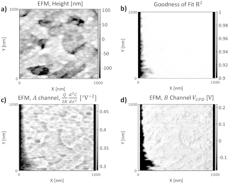
The tested metal is a thin layer of Indium Tin Oxide deposited on a glass substrate (Buwon Act Co. Ltd, China). Figure 1 shows the following channels: a) height; b) goodness of fit R2; c) deconvolved channel proportional to the second derivative of the tip-sample capacitance A = (Q/2K)∂2C/∂z2 [°V−2]; d) deconvolved channel corresponding to the tip-sample contact potential difference VCPD [V]. The typical granular shape of ITO can be observed in the height (Figure 1a), capacitive channel A (Figure 1c), and contact potential difference channel B (Figure 1d). As shown in Figure 1b, most of the pixels of the deconvolved channels have a goodness of fit R2 above 0.98. The terraces consisting of layers of crystalline ITO, seen in the height channel, cannot be observed in the capacitance and VCPD channels, which appear as a flatter surface in comparison to the height channel.
Figure 1. ITO probed by SPP-EFM.
(a) Height [nm]. (b) Goodness of fit R2. (c) Deconvolved channel proportional to the second derivative of the tip-sample capacitance (Q/2K)∂2C/∂z2 [°V−2]. (d) Deconvolved channel corresponding to the tip-sample contact potential difference VCPD [V].
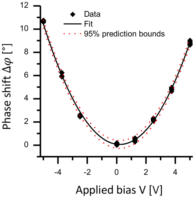
Figure 2 shows an example of a local calibration curve build from 86 (V, Δφ) data points extracted from a single ITO grain. The fitting parabola a(V − b)2 matches well the experimental data points, and confirms that the choice of −5 V and 5 V as the maxima of the sweeping voltage keeps the data points within a parabolic regime. The fitted coefficient are a = (Q/2K)∂2C/∂z2 is 0.383 ± 0.004 [°V−2] and b = VCPD = 0.18 ± 0.01 [V]. Here, the standard errors correspond to the 95% confidence bounds. In Figure 2, the confidence bounds are also used to plot the 95% prediction bounds.
Figure 2. Calibration parabola build from 86 (V, Δφ) data points extracted from a homogenous region consisting of a single ITO grain.
The 95% prediction bounds are shown in the plot. Fitted values are: a = 0.383 [°V−2] and b = 0.18 [V]. Standard errors based on 95% prediction bounds are: Ea = 0.004 [°V−2] and Eb = 0.01 [V].
The height, the capacitance and the VCPD data can be compared by calculating the correlation coefficient ρ between their normalized values. Height and capacitance are negatively correlated (ρ = −0.75). Height and VCPD are uncorrelated (ρ = 0.27), as well as capacitance and VCPD (ρ = 0.06). This is due to the fact that the capacitive signal depends on the tip sample geometry, while the VCPD is independent from the sample topography in a homogeneous sample. This observation also excludes the presence of topographical artifacts in the VCPD signal.
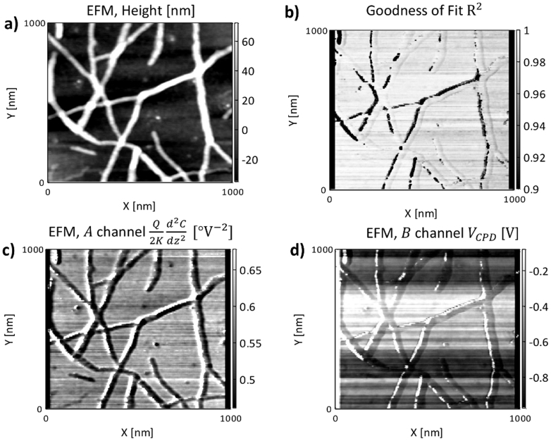
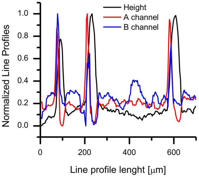
Poly(3-hexylthiophene-2,5-diyl) nanowires dispersed in anisole (purity 99%, Sigma-Aldrich, UK) were spincoated on a Si/SiO2 substrate and annealed for 30 minutes at 140°C. As shown in Figure 3, the wires have an average width and a thickness of ~60 nm. Figure 4 shows the following normalized channels: height, capacitance (Channel A) and VCPD (Channel B). The height line profile is not correlated with the capacitance (ρ = 0.02) and the VCPD (ρ = 0.12) line profiles, while capacitance and VCPD are highly correlated (ρ = 0.6). This is because the sample is heterogeneous (both Si substrate and nanowires are imaged simultaneously). The drift in the VCPD, along the y-scan direction (top-bottom), could be an effect of tip contamination24. However, VCPD contrast is visible between wires and substrate because of their strong difference in work-function. Values of VCPD at the left borders of the nanowires are affected by high error, as shown by the goodness of fit channel. This could be due to asymmetries in the tip shape or hysteresis of the piezo, resulting in discrepancies between trace and retrace channels, in correspondence of sharp features. In the case of the piezo hysteresis, this effect could be probably avoided by performing the technique with just one trace or retrace channel, at the expense of losing in resolution and doubling the time required for a scan38.
Figure 3. P3HT nanowires probed by SPP-EFM.
(a) Height [nm]. (b) Goodness of fit R2. (c) Deconvolved channel proportional to the second derivative of the tip-sample capacitance A = (Q/2K)∂2C/∂z2 [°V−2]. (d) Deconvolved channel corresponding to the tip-sample contact potential difference VCPD [V].
Figure 4. Line profile across three P3HT nanowires probed by SPP-EFM, showing the following normalized channels: height, = (Q/2K)∂2C/∂z2 [°V−2], and B = VCPD [V].
The possibility to simultaneously map and correlate height, capacitance and VCPD channels could be helpful for nanowires film thickness optimization, during the development of organic transistors. Once properly calibrated with the height channel, the capacitance and the VCPD channel could be used to measure the number of stacked nanowires in a densely packed nanowires film. Datta et al. recently demonstrated this approach in an EFM-sweep study of a Few Layers of Graphene (FLG) deposited on an insulating substrate of SiO2/Si31.
Discussion
We have reported a technique for mapping Electrostatic Force Microscopy (EFM) sweep data into 2D images. The method allows simultaneous probing, in the same scanning area, of the contact potential difference and the second derivative of the capacitance between tip and sample, along with the height information. We designate this approach as the Scanning Probe Potential Electrostatic Force Microscopy (SPP-EFM) technique. In line with the recent challenges of simultaneous multi-information extraction, the SPP-EFM technique presents a simple solution for concurrently obtaining information similar to the one that could be recorded with two different techniques: Scanning Capacitance Microscopy (SCM) and Kelvin Probe Force Microscopy (KPFM). The SPP-EFM technique combines the advantages of lift-mode EFM-phase method, such as the superior lateral resolution when compared to lift-mode KPFM, and EFM-sweep, such as the quantitative measurements. Implemented with a microscope that can be operated in lift-mode EFM-phase, SPP-EFM is a low-cost technique that does not require any expensive extra lock-in amplifiers.
The enabling component of the SPP-EFM technique is the SPP-EFM-GUI, a graphical user interface we developed under MATLAB, for image acquisition, processing and analysis. The SPP-EFM works with both Nanoscope and Asylum Research raw data files. It can also be used for basic AFM image analysis. The SPP-EFM is an open-source software, which can be freely downloaded from the supporting information (with a video tutorial and example files).
Finally, we have shown two examples of SPP-EFM analysis. Among its several applications, the SPP-EFM technique has the potential of deconvolving EFM data into contact potential images of polymer-fullerene blends for organic solar cells applications, showing a contrast between the polymer and the fullerene phase. This would not be possible with lift-mode KPFM due to its limitations in the lateral resolution. The possibility of locally discriminating between the two materials on the nano-scale would be beneficial for a better understanding of the nano-morphology of films for organic electronics applications.
Methods
SPP-EFM: system setup
Scanning Probe Potential Electrostatic Force Microscopy (SPP-EFM) measurements are performed in ambient conditions with a Nanoscope III Multimode with Extender electronics module (Bruker, USA). The Nanoscope allows recording only three channels. In order to deconvolve the lift-mode EFM-phase images, represented by Δφ in equation (6), into a VCPD image (b) and a capacitive image (a), two channels are used: EFM-phase trace and EFM-phase retrace, both in lift mode.
Commercial highly doped n++ Super-Sharp tips (Nanosensors, Switzerland, nominal tip radius 2 nm) are used9,24 for the scans. Before starting a scan in SPP-EFM mode, several scans in AFM mode (light tapping) are taken9,24. Usually after ~3 hours of AFM scans, the x and y piezo drift is minimized. Minimum drift is a necessary condition in SPP-EFM: trace and retrace line scans must be almost coincident.
As suggested by Lei9,24 and Simmonds34, we used a fixed tip-sample distance of 20 nm during the lift-mode scan. At this distance, lift-mode EFM-phase provides higher lateral resolution than the lift-mode KPFM9,24, which directly probes VCPD.
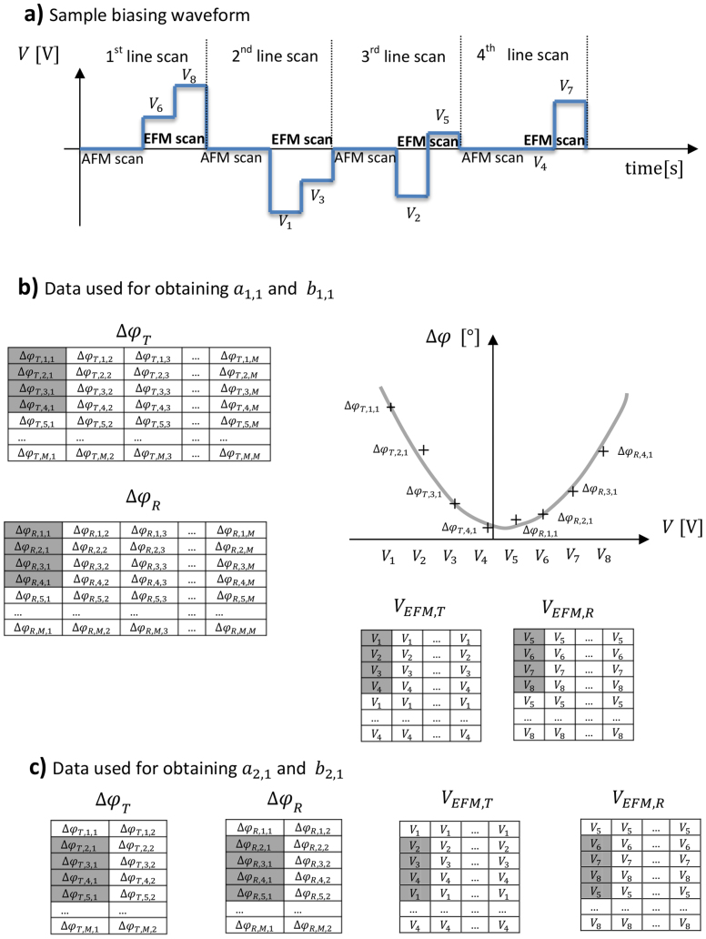
SPP-EFM: sample biasing waveform
The biasing waveform can either be applied via the AFM control software or with an external waveform generator. A line scan in lift-mode EFM-phase is made of 4 contributions: AFM trace and retrace, EFM trace and retrace. The tip is always grounded, and a voltage waveform is applied to the sample. During the AFM trace and retrace the bias applied to the sample is zero, while during the lift-mode non-zero biases are applied. Several waveform combinations have been tested. When linear voltage sweeps9,24,34 are used in a single line (for example a saw tooth waveform), the sensed bias cannot follow exactly the applied bias, probably due to capacitive effects. In order to avoid these problems, a varying bias during the lift-mode scan should be avoided. The best results have been obtained by maintaining a constant voltage in each EFM line scan. The optimized sample biasing waveform used in the present work is shown in Figure 5a. The trace raster scan is made of 512 × 512 pixels. Each raster point corresponds to one element of the biasing matrix VEFM,T, shown in Figure 5b. Each column of VEFM,T is divided into the 4-elements vector VEFM,T,u = [V1 V2 V3 V4]T, where each element corresponds to a different applied bias. This vector repeats along the column as shown in Figure 5b–c. This biasing scheme is then repeated for all columns, in order to have a constant voltage along each EFM line scan. At each raster scan point, Δφ is measured. This gives a phase difference matrix indicated as ΔφT. An analogous biasing scheme is employed for the retrace raster scan. However, in this case, a different 4-elements biasing vector VEFM,T,u = [V5 V6 V7 V8]T is applied. We refer to the biasing matrix as VEFM,T,R, and to the measured phase difference matrix as ΔφR (Figure 1b–c).
Figure 5. Sample biasing scheme.
(a) Sample biasing waveform. (b) Basic principle of SPP-EFM local calibration for the first pixels of the A and B channels. The 8 values from the lift-mode EFM-phase trace and retrace channels are plotted vs. the applied bias and then fitted by using the previously described parabola. (c) Generation of the pixel (2,1) for A and B channels.
In most of the scans, an AFM scan rate of 1 Hz is used. The waveform maximum amplitude is set to ±5 V, in order to have a nearly perfect parabolic relationship. Larger biases result in strong deviations of Δφ. The EFM channel parameters in the Nanoscope software must be set in a way that no automatic flattening is applied to the acquired EFM-phase images34.
SPP-EFM: software design and data processing
Once the scan has been completed, height, lift-mode EFM-phase trace and retrace channels are automatically saved in a Nanoscope raw data file by the Nanoscope software. An open-source graphical user interface software (SPP-EFM GUI) has been developed with MATLAB for SPP-EFM data acquisition and processing, and is freely available, with a video tutorial and example files, in the supporting information. The software was initially developed for processing Nanoscope binary files, but is currently also able to process Asylum Research binary files.
Multiple Nanoscope binary raw data files can be imported and converted into height and EFM-phase data and visualized in the software. Information on the scan (header) is automatically imported from the binary file by using regular expressions. Workflow sessions can be saved and reloaded. Images can be zoomed, panned, contrast-adjusted, and saved in a ready-to-publish vectorial file format. Multiple line profiles from all the channels can be extracted along a line and plotted.
The objective of the fitting routine in the SPP-EFM technique is to deconvolve the two EFM-phase images into 3 main extra channels (2D images): A, the capacitive contribution (from the a parameters in equation (6)); B, the VCPD contribution (from the b parameter in equation (6)); and R2, the goodness-of-fit. Further channels representing the fitting error on the a and b parameters are also available. The deconvolution scheme for the first pixel (1, 1) of the 3 new channels is descibed in Figure 5b. The deconvolution scheme for the pixel (2, 1) of the 3 new channels is described in Figure 5c. In general, the (i, j)-th pixel of the A and B channels, where i and j are respectively the row and column indexes, is obtained by fitting the following (V, Δφ) points:
 |
where j is fixed and i: i + 3 indicates the following rows: i, i + 1, i + 2, i + 3. Each step involves a parabolic fitting with the MATLAB function fit. It is clear from equation (7), that the fitting scheme consists of a ‘moving average' along the columns, with an averaging window of 4 pixels. Therefore some of the EFM lateral resolution along the y-scan direction is lost. However, no information is lost along the x-scan direction. The resolution loss along the y-direction could be improved (on a different AFM system) by simply increasing the number of pixels per image, at the price of a lower scan speed (and a higher drift). Further details about the fitting scheme are reported in the supporting information. Since images are acquired with a resolution of 512 × 512 pixels, the number of fitting steps is equal to 262,144. Parallel computing is used to speed up the computation. Multiple images can be batch deconvolved.
After the deconvolution is completed, 3 new extra main channels appear: A = (Q/2K)∂2C/∂z2, B = VCPD, and R2. Secondary channels displaying the fit error on A and B are also available. Local calibration curves can be built by drawing arbitrary shapes around features of interest in any channel. In this way, the average A and B parameters related to that region are extracted. Statistics about each single channel can be extracted by selecting data resulting only from a good fit, i.e. by using the R2 information. A R2 threshold value of 0.99, for example, extracts only the pixels with R2 > 0.99, and creates an image mask which is applied to the desired channel to extract statistic information. Using the created mask, the histogram of the current channel can be extracted and displayed in the edit box. This procedure can be batch applied to multiple files.
Finally a significant improvement of our method could be achieved by integrating it with the ECM technique proposed by Riedel et al.21,22,23 for the conversion of the A = (Q/2K)∂2C/∂z2 channel into a map of the dielectric permittivity.
All the mathematical steps, from the basic mass-spring-damper (representing the cantilever dynamics) to the expression of the phase shift Δφ probed in EFM mode, are shown in a rigorous and simple way in the supporting information. The SPP-EFM-GUI, the graphical user interface we developed under MATLAB, for image acquisition, processing and analysis, can be downloaded from The software can be downloaded from: http://www.lilliu.co.uk/toolboxes/SPM/SPC-EFM_GUI.zip. A video tutorial on the SPP-EFM-GUI is available at the following link: http://www.youtube.com/watch?v=yQWIAyBhFO0.
Author Contributions
S.L. and C.M. developed the technique, carried on the experiments, prepared the figures, and wrote the main manuscript. M.H. prepared the P3HT nanowires samples. J.E.M. and M.S.D. supervised the project. M.S., M.C. and M.E. helped with the theoretical development of the technique.
Supplementary Material
Supporting Information
Acknowledgments
This work was partially funded by the Engineering and Physical Sciences Research Council (EPSRC, grant number EP/F016255), granted for the UKOPV collaboration (Cardiff University, Sheffield University, Cambridge University, Diamond Light Source).
References
- Martin Y. et al. High-resolution capacitance measurement and potentiometry by force microscopy. Appl. Phys. Lett. 52, 1103–1105 (1988). [Google Scholar]
- Bürgi L. et al. A microscopic view of charge transport in polymer transistors. Synthetic Met. 146, 297–309 (2004). [Google Scholar]
- Bürgi L. et al. Close look at charge carrier injection in polymer field-effect transistors. J. Appl. Phys. 94, 6129–6137 (2003). [Google Scholar]
- Bürgi L. et al. Noncontact potentiometry of polymer field-effect transistors. Appl. Phys. Lett. 80, 2913–2915 (2002). [Google Scholar]
- Ong B. S. Design of high-performance regioregular polythiophenes for organic thin-film transistors. P. IEEE 93, 1412 (2005). [Google Scholar]
- Coffey D. C. et al. Time-resolved electrostatic force microscopy of polymer solar cells. Nat. Mater. 5, 735–740 (2006). [DOI] [PubMed] [Google Scholar]
- Visoly-Fisher I. et al. How Polycrystalline Devices Can Outperform Single-Crystal Ones: Thin Film CdTe/CdS Solar Cells. Adv. Mater. 16, 880 (2004). [Google Scholar]
- Bachtold A. et al. Scanned Probe Microscopy of Electronic Transport in Carbon Nanotubes. Phys. Rev. Lett. 84, 6082 (2000). [DOI] [PubMed] [Google Scholar]
- Lei C. H. et al. Conductivity of macromolecular networks measured by electrostatic force microscopy. Appl. Phys. Lett. 83, 482–484 (2003). [Google Scholar]
- Lu Y. et al. Electrostatic Force Microscopy on Oriented Graphite Surfaces: Coexistence of Insulating and Conducting Behaviors. Phys. Rev. Lett. 97 (2006). [DOI] [PubMed] [Google Scholar]
- Williams C. C. et al. Lateral dopant profiling with 200 nm resolution by scanning capacitance microscopy. Appl. Phys. Lett. 55, 1662–1664 (1989). [Google Scholar]
- Nonnenmacher M. et al. Kelvin probe force microscopy. Appl. Phys. Lett. 58, 2921–2923 (1991). [Google Scholar]
- Girard P. Electrostatic force microscopy: principles and some applications to semiconductors. Nanotechnology 12, 485 (2001). [Google Scholar]
- Aoki N. et al. Scanning gate microscopy of copper phthalocyanine field effect transistors. Appl. Phys. Lett. 91, 192113 (2007). [Google Scholar]
- Saurenbach F. et al. Imaging of ferroelectric domain walls by force microscopy. Appl. Phys. Lett. 56, 1703–1705 (1990). [Google Scholar]
- Kalinin S. V. et al. Local potential and polarization screening on ferroelectric surfaces. Phys. Rev. B 63, 125411 (2001). [Google Scholar]
- Garcĺa R. et al. Dynamic atomic force microscopy methods. Surf. Sci. Rep. 47, 197–301 (2002). [Google Scholar]
- Elings V. B. et al. Scanning probe microscope using stored data for vertical probe positioning. (1994).
- Jacobs H. et al. Surface potential mapping: A qualitative material contrast in SPM. Ultramicroscopy 69, 39–49 (1997). [Google Scholar]
- Fumagalli L. et al. Dielectric-constant measurement of thin insulating films at low frequency by nanoscale capacitance microscopy. Appl. Phys. Lett. 91, 243110 (2007). [Google Scholar]
- Riedel C. et al. Nanoscale dielectric properties of insulating thin films: From single point measurements to quantitative images. Ultramicroscopy 110, 634–638 (2010). [DOI] [PubMed] [Google Scholar]
- Riedel C. et al. Determination of the nanoscale dielectric constant by means of a double pass method using electrostatic force microscopy. J. Appl. Phys. 106, 024315 (2009). [Google Scholar]
- Riedel C. et al. Nanodielectric mapping of a model polystyrene-poly(vinyl acetate) blend by electrostatic force microscopy. Physical Review E 81, 010801 (2010). [DOI] [PubMed] [Google Scholar]
- Lei C. H. et al. Quantitative electrostatic force microscopy-phase measurements. Nanotechnology 15, 627 (2004). [Google Scholar]
- Paris D. T. et al. Basic Electromagnetic Theory. (McGraw Hill, 1969). [Google Scholar]
- Feynman R. P. et al. The Feynman Lectures on Physics. (Addison-Wesley Publishing Company Inc., 2011). [Google Scholar]
- Maragliano C. et al. Dynamic electrostatic force microscopy technique for the study of electrical properties with improved spatial resolution. Nanotechnology 24, 225703 (2013). [DOI] [PubMed] [Google Scholar]
- Gekhtman D. et al. Electrostatic Force Spectroscopy and Imaging of Bi Wires: Spatially Resolved Quantum Confinement. Phys. Rev. Lett. 82, 3887 (1999). [Google Scholar]
- Burnett T. et al. Mapping of Local Electrical Properties in Epitaxial Graphene Using Electrostatic Force Microscopy. Nano Lett. 11, 2324–2328 (2011). [DOI] [PubMed] [Google Scholar]
- Aykutlu D. et al. Electrostatic force spectroscopy of near surface localized states. Nanotechnology 16, S125 (2005). [Google Scholar]
- Datta S. S. et al. Surface Potentials and Layer Charge Distributions in Few-Layer Graphene Films. Nano Lett. 9, 7–11 (2008). [DOI] [PubMed] [Google Scholar]
- Cockins L. et al. Spatially resolved low-frequency noise measured by atomic force microscopy. Phys. Rev. B 79, 121309 (2009). [Google Scholar]
- Piarristeguy A. A. et al. High resolution electrical characterisation of Ag-conducting heterogeneous chalcogenide glasses. Solid State Ionics 181, 1205–1208 (2010). [Google Scholar]
- Simmonds H. et al. Self-assembled organic nanowires: A structural and electronic study. J. Vac. Sci. Technol. B 27, 831–835 (2009). [Google Scholar]
- Lilliu S. et al. Inkjet-printed organic photodiodes. Thin Solid Films 520, 610–615 (2011). [Google Scholar]
- Lilliu S. et al. The Influence of Substrate and Top Electrode on the Crystallization Dynamics of P3HT:PCBM Blends. Energy Procedia 31, 60–68 (2012). [Google Scholar]
- Lilliu S. et al. Effects of Thermal Annealing Upon the Nanomorphology of Poly(3-hexylselenophene)-PCBM Blends. Macromol. Rapid Commun. 32, 1454–1460 (2011). [DOI] [PubMed] [Google Scholar]
- Ziegler D. et al. Improved accuracy and speed in scanning probe microscopy by image reconstruction from non-gridded position sensor data. Nanotechnology 24, 335703 (2013). [DOI] [PubMed] [Google Scholar]
Associated Data
This section collects any data citations, data availability statements, or supplementary materials included in this article.
Supplementary Materials
Supporting Information


