Abstract
Nanoscale biosensors have remarkable theoretical sensitivities, but often suffer from sub-optimal limits of detection in practice. This is in part because the sensing area of nanoscale sensors is orders of magnitude smaller than the total device substrate. Current strategies to immobilize probes (capture molecules) functionalize both sensing and non-sensing regions, leading to target depletion and diminished limits of detection. The difference in topography between these regions on nanoscale biosensors offers a way to selectively address only the sensing area. We developed a bottom-up, topographically selective approach employing self-assembled poly(N-isopropylacrylamide) (PNIPAM) hydrogel nanoparticles as a mask to preferentially bind target to only the active sensing region of a photonic crystal (PhC) biosensor. This led to over one order of magnitude improvement in the limit of detection for the device, in agreement with finite element simulations. Since the sensing elements in many nanoscale sensors are topographically distinct, this approach should be widely applicable.
INTRODUCTION
The detection of biomedically significant molecules with high-sensitivity nanoscale optical sensors has been the focus of major development efforts by many research groups worldwide.1 Novel structures resulting from these efforts, including ring- and whispering-gallery resonators,2,3,4 waveguides,5,6,7 and photonic crystals8,9 operate by resolving minute changes in refractive index that occur when a target molecule or virus interacts with the device. While all of these devices have remarkable theoretical sensitivities, their observed limits of detection (LoD) under real-world conditions are often unsatisfactory.1,10
The LoD of a biosensor is dependent not only on the sensitivity of the transduction mechanism, but also on the biomolecular thermodynamics of the immobilized probe and the target analyte in solution.11,12 In addition to presenting unique challenges for analyte mass transport, nanoscale sensors require careful functionalization with capture molecules (for example, antibodies) since the active sensing region is orders of magnitude smaller than the overall device. If the placement of capture molecules (probes) onto the surface is indiscriminate and both the sensing and non-sensing regions are functionalized,13,14 the target loss to the non-sensing regions may become substantial enough to disturb the bulk concentration of target. This can lead to a lower fraction of material being bound to the sensing area, and a higher (worse) LoD.15,16,17 Conventional passivation techniques18 involving incubation with proteins (e.g. bovine serum albumin) or synthetic blocking chemicals cannot be used to avoid this issue, since they would result in equal application to the non-sensing and sensing areas of nanoscale devices. A common top-down approach to this problem has been to shrink the size of the probe droplet in manufacturing to closely overlay only the active sensing region.19,20 However, there are considerable challenges with alignment and uniform dispensing on such a small scale. Others have exploited material differences within a nanoscale biosensor. For example, Fuez et al. showed material-selective surface chemistry that selectively bound a blocking agent to inactive titanium dioxide surfaces of a plasmonic nanostructure leaving the gold sensing region to bind biomolecules.21 Since incorporation of different materials into the device isn’t always feasible, alternative strategies are clearly needed.
An alternative to “top down” methods for nanoscale functionalization is to employ a “bottom up”, or self-assembly approach. Successfully applying a bottom-up approach requires some method of differentiating the area to be functionalized (the active sensing area of the sensor) from the remaining area. We hypothesized that the topographical features of nanoscale sensors could present a readily accessible strategy to accomplish this, as the active sensing area is topographically distinct from the remainder of the device. Here we report a novel bottom-up technique in which topographically selective assembly of PNIPAM hydrogel nanoparticles differentiates between active (sensing) and inactive (non-sensing) areas to selectively functionalize nanoscale sensors. Demonstrated in the context of a 2-D photonic crystal sensor, we show that this strategy provides at least an order of magnitude improvement in LoD relative to nonselective functionalization, a value consistent with theory.
EXPERIMENTAL SECTION
Photonic Crystal Design
The PhC design used in the current study has been described before.22 Briefly, the 2D PhC slab structure consists of a 25 × 26 array of air wells in a triangular lattice pattern with row of wells removed from the center creating a w1 waveguide (line defect). A nanocavity was created by modifying the radius of a single air well adjacent to the waveguide (point defect).
Device Fabrication
A p-type silicon-on-insulator (SOI) wafer (<100>) with a 450 nm silicon device layer on top of 1 µm thick buried silicon oxide (BOX) was used as the starting substrate for the PhCs.
PMMA Fabrication
A 130 nm oxide hard mask was thermally grown on the Si layer via wet oxidization. Polymethylmethacrylate (PMMA) was used as an e-beam resist and a JEOL JBX-6300FS system was used to write the PhC patterns. The pattern was developed and dry etched using argon assisted CHF3 gas in a reactive-ion-etcher to transfer the oxide hard mask, followed by a gas etch with CF4 and BCl3 to etch the Si device layer. The individual PhC devices were cleaved with a diamond scribe to create smooth waveguide facets to facilitate light coupling.
HSQ Fabrication
The native oxide layer of the SOI substrate was stripped using a buffered oxide etch (6:1 hydrofluoric acid/ammonium fluoride). Hydrogen silsesquioxane (HSQ) was used as an e-beam resist and a JEOL JBX-6300FS system was used to write the PhC patterns. After exposure, the pattern was developed and transferred using a CF4 and BCl3 gas etch. The individual PhC devices were cleaved with a diamond scribe to create smooth waveguide facets to facilitate light coupling.
Finite Element Modeling
All solutions were generated using COMSOL Multiphysics (v.4.2a). Bulk diffusion was modeled using the Transport of Diluted Species module. Surface reactions were modeled using General Form Boundary PDEs.
Optical Set-up
A tunable laser (Hewlett Packard, model 8168F, output power: −7 to 7 dBm) operating within the wavelength range of 1440–1590 nm was used to scan and optically probe the 2D PhC device, with a wavelength resolution of 0.05 nm. A polarization controller was used to excite the TE modes and light was coupled through tapered ridge waveguides into the PhC device using a tapered lensed fiber (Nanonics, Israel). The transmitted optical power was measured using an indium gallium arsenide (InGaAs) photodiode detector (Teledyne Judson Technologies, PA, USA).
Nanoparticle Synthesis
Poly(N-isopropylacrylamide) microgels were prepared via free radical precipitation polymerization. The monomers N-isopropylacrylamide (0.76 g) and bis-acrylamide (BIS) (0.013 g) were dissolved in 50 mL of double distilled water (ddH2O) inside of a 500 mL 3-neck flask. The solution was then mixed with 0.34 mL of aqueous 1% (SDS). The flask containing the solution was equipped with a nitrogen line, overhead stirrer, and gas outlet. The solution was bubbled with nitrogen for 45 minutes to remove dissolved oxygen. The mixture was heated to 60 °C and a solution of 0.0166 g of ammonium persulfate was dissolved in 0.5 mL of water and injected into the flask to start the reaction. The reaction proceeded for 5 hours in an inert atmosphere at a constant stir rate of 200 RPM. After 10 minute the solution became visibly turbid, which was indicative of particle formation. At 5 hours, the flask was removed from heat opened to ambient oxygen while maintaining a constant stir-rate for 15 minutes. The solution was filtered through a 1.2 µm cut-off syringe filter (Millipore). The purified solution was used as is.
Nanoparticle Dipcoating
Both the flat silicon dioxide and nanostructured SOI chips were dipcoated using a syringe pump (Yale Apparatus YA-12) which was modified to hold a pair of tweezers and mounted vertically. The chips were dipped into a 1:100 v/v dilution of PNIPAM particles in double distilled water at a speed of 500 µm per minute until the chip was submerged in solution to approximately half the height of the chip (0.2 – 0.5 cm, depending on the chip length). The pump was stopped for 30 seconds to allow the chip to equilibrate with the solution before being pulled out at a rate of 1000 µm per minute. Once the chips had cleared the water line, the edges of the chip were inspected to ensure they were completely dry before removing them.
Aminosilane-glutaraldehyde surface functionalization
In order to generate a protein-reactive surface, both planar silicon oxide and SOI chips were functionalized with glutaraldehyde (GA) as per the following protocol. First, the chips were cleaned in piranha solution (3:1 (v/v) conc. sulfuric acid to 30% hydrogen peroxide CAUTION: piranha solution reacts vigorously with organic materials and must be used with care) for 30 minutes, followed by de-ionized distilled water rinse and dried under a stream of nitrogen gas. Next, they were incubated with a 1% (v/v) solution of (3-aminopropyl)dimethylethoxysilane in anhydrous toluene for 20 minutes on an orbital shaker. The chips were then repeatedly washed with anhydrous toluene, dried under a stream of nitrogen and baked at 110 °C for 30 minutes. After the chips had cooled to room temperature (approximately 5 minutes), a solution of 1.25% (v/v) GA in modified PBS buffer (MPBS: 10mM NaH2PO4, 10 mM Na2HPO4, 150 mM NaCl at pH 7.2) was poured over them, and the chips were left in this solution on a shaker for 60 minutes. Afterwards, they were washed with MPBS and ddH2O and dried under a nitrogen stream.
Antibody Localization on Planar Silicon Oxide Chips
Planar square silicon oxide chips (1 cm × 1 cm) were washed in piranha and functionalized with GA as described above. The chips were carefully dipcoated with PNIPAM nanoparticles such that half of each chip was passivated while the other half remained protein reactive. Next, the chips were incubated with three different concentrations of rhodamine-labeled IgG (0.1 µM, 0.5 µM and 1 µM) for 60 minutes. Lastly, the chips were washed with MPBS-ET (MPBS buffer with 3 mM Ethylenediaminetetraacetic acid and 0.05% (v/v) Tween-20) for 30 minutes, rinsed with ddH2O and imaged with epifluorescence.
Epifluorescence Microscopy
The fluorescent intensity of the passivated and un-passivated areas of the planar silicon oxide chips was evaluated with an Olympus-BX60 microscope with a Qicam FAST-1394 (Qimaging) active cooled CCD camera. A silicon dioxide chip with no fluorophore was used as a control to measure the background fluorescence. The exposure time was kept constant at 2 seconds. Data analysis was performed with ImageJ (NIH).23 The relative fluorescence intensity (RFI) was calculated as:
where are the unmasked, masked, and control average fluorescence intensities, where “control” indicates a “background” chip with identical surface chemistry but not exposed to rhodamine-labeled IgG. The error bars for each condition were computed as the relative fluorescence intensity multiplied by the square root of the sum of the squares of the normalized standard deviations (standard deviation/mean) of the masked and unmasked portions of the chip, and a control chip with no fluorophore:
where SDRFI is the calculated error, SDFU, SDFM, and SDFC are the standard deviations of unmasked, masked, and control fluorescence intensities respectively.
Antibody Localization on PhC Chips
Newly fabricated PhC chips were thermally oxidized in a furnace with an oxygen gas stream at 900 °C for 15 minutes. The chips were then functionalized with aminosilane-glutaraldehyde chemistry. Next, the PhC chips were dipcoated with PNIPAM particles at a rate of 1000 µm min−1. After passivation, a 10 µL droplet of 0.1 µM IgG in MPBS buffer was placed on the chip covering the PhC sensing region. The chips were then placed in a humidity chamber for 1 hour (no evaporation appeared to occur), allowing the human-IgG to covalently bind to the exposed GA groups via amine-aldehyde coupling chemistry (Schiff base formation). After antibody immobilization, the remaining aldehyde groups were blocked by incubating the chips in 0.66 mg mL−1 (~10 µM) BSA solution in HBS buffer (20 mM 2-[4-(2-hydroxyethyl)piperazin-1-yl]ethanesulfonic acid (HEPES), 150 mM NaCl, at pH 7.2) for 1 hour. The chips were then washed with MPBS, dried under nitrogen stream and incubated with a 10 µL droplet of the target solution (anti-IgG) at increasing concentrations diluted in MPBS buffer for a period of 1 hour. Finally, the chips were washed with MPBS-ET for 30 min on an orbital shaker, rinsed with ddH2O and dried under a stream of nitrogen. The chips were then subjected to optical characterization.
Peak Fitting and Data Analysis
After spectra collection, each data set was filtered using Origin (OriginLab, Northampton, MA). A fast Fourier transform low-pass filter with a frequency cut-off of 0.5 was used to remove high frequency noise. The peaks were then fit to the Lorentz equation with transmission intensity (a.u.) plotted as a function of wavelength (nm):
The fitted value of xc (represented in units of wavelength) was used as the location of the minimum absorption for the data-set.
RESULTS AND DISCUSSION
Numerical simulations
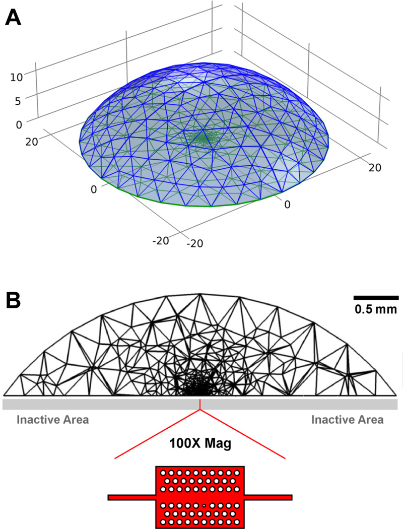
While it is a logical hypothesis that antibody localization to active areas of a nanoscale device will enhance the limit of detection, we first tested this assertion through simulation using finite element methods. The geometry used was a section of a sphere, representing a water droplet with a contact angle of 55 degrees and a volume of approximately 10 µL (Figure 1A). The flat region of the sectioned sphere was composed of a 70 µm2 area circle (active region) surrounded by a circular contact surface with a 4.5 mm diameter (inactive region). Due to the large size difference between the two areas, a much finer volume (tetrahedral) mesh was required near the active site, which was located at the center of the flat region (Figure 1B).
Figure 1.
Geometry and meshing of a droplet with “active” (sensing) and “inactive” (non-sensing) areas for finite element simulations. The surface mesh (A) is plotted on a 10−4 m scale, while the mesh in (B) is a cross-section of the geometry volume, shown on a scale of 0.5 mm. Sensor (active) area is indicated by the red line at the center of (B), and in 100x expansion.
The surface reaction was modeled as immunoglobulin gamma (IgG) binding to antiimmunoglobulin gamma (anti-IgG) with 1:1 binding stoichiometry. The surface density of antibody sites was assumed to be a monolayer with a value of 1.2 × 10¹² antibodies cm−2. The kon and koff values were 250 m3s−1mol−1 and 0.0003 s−1, respectively. The diffusion coefficient for IgG was modeled as 5 × 10⁻¹¹ m2 s−1. The following diffusion equation was solved for the entire domain:
| (1) |
where c and D are the bulk analyte concentration (mol m−3) and diffusion coefficient of the target (m2 sec−1), respectively. Boundary conditions representing the flux balance between the surface and bulk concentrations of target species were set for the active (sensing) and inactive areas:
| (2) |
where n is a unit vector normal to the reaction surfaces, Rcs is the inward flux of the target into the bulk (can be either positive or negative), kon and koff are the kinetic on (m3 sec−1 mol−1) and kinetic off (s−1) rate constants for a target and capture-molecule pair, cs is the surface concentration of bound target (mol m−2), θmax is the maximum surface concentration of available binding sites (mol m−2) which was explicitly set at the active and inactive regions, and e is an efficiency factor for antibody localization (dimensionless). The active boundary, representing the “nanoscale sensor” was modeled with an efficiency factor of 1 (e=1) implying that the active region had the maximal surface density of antibodies. The efficiency factor on the inactive boundaries was set to one of three values: e=0 for perfect antibody localization (ABL) (no antibodies at the inactive region), e=0.05 for 95% ABL (surface density of antibody at the inactive region was 5% of the value at the active region), and e=1 for no ABL (the inactive area had the same surface density of antibodies as the active area).
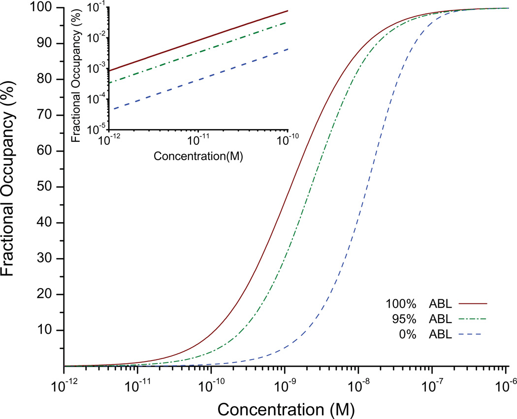
Dose-response curves (Figure 2) were generated by plotting fractional occupancy of target, at the active region for different concentrations of analyte after 24 hours of simulated incubation. The results show a marked difference in the location and shape of the dose-response curve for perfect ABL (e=0), partial ABL (e=0.05), and no ABL (e=1). An assumption of perfect ABL produces a dose-response curve whose midpoint lies at the IgG / anti-IgG equilibrium constant, as expected (at 50% surface coverage, the concentration value matches the expected equilibrium constant, ). Simulations suggest that even a 95% ABL provides a 10-fold higher surface coverage at the active sensing area relative to the case with no ABL (Figure 2 inset). Thus, these simulations predict that ABL with a nanoscale sensor will generate a significantly higher signal compared to a sensor with no ABL at the same analyte concentration, thereby improving the limit of detection.
Figure 2.
Simulated dose-response curves at 100% ABL (red solid line), 95% ABL (green dot-dash line), and 0% ABL (blue dashed line). The inset highlights the low-concentration regime of the dose response, plotted on a log/log scale.
2D photonic crystal biosensor operation
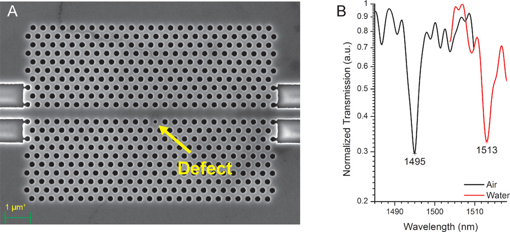
To test these predictions experimentally, we used a 2-dimensional photonic crystal (2D PhC) biosensor previously employed by our group to detect proteins22 and virus-like particles24. The active sensing area of this device is approximately 7 µm by 10 µm and consists of 509 cylindrical wells in silicon with a diameter of 220 nm and a single cylindrical well 150 nm in diameter, with all wells etched to depths of ~ 400 nm. A w1 waveguide allows propagation of guided modes within the photonic band-gap (PBG) of the crystal. Light is confined within the embedded silicon (Si) layer by total internal reflection from the encasing silicon oxide (SiO2), which has a lower refractive index. Breaking the translational symmetry by modifying the radius of a well to create a defect (Figure 3A), gives rise to a localized mode within the PBG. Thus, the w1 waveguide photonic crystal allows light transmission at all frequencies except at the resonant defect nano-cavity wavelength, resulting in a characteristic sharp dip in its transmission spectrum. The electric field is strongly confined in the defect at resonance. Analyte binding causes the local refractive index to change resulting in a red-shift of the resonant wavelength due to the strong light-matter interaction within the defect. Figure 3B depicts the red shifts observed due to the refractive index change when a 2D PhC sensor is analyzed in air (n~1.0) followed by water (n~1.32 at 1550 nm wavelength).
Figure 3.
(A) Scanning electron microscope (SEM) image of a 2D PhC device (10 µm × 7 µm) with an array of wells (radius = 111 nm) etched in a triangular lattice. A row of wells was removed to create a w1 waveguide. A defect (radius = 73 nm) (yellow arrow) disrupts the periodicity, giving rise to an absorption peak. (B) Low-pass filtered transmission spectra for air (n~1) and water (n~1.32) show a peak shift to longer wavelengths upon hydration, demonstrating the RI sensitivity of the 2D PhC.
Antibody surface coverage evaluation and localization with PNIPAM nanoparticle mask
PNIPAM is versatile and can be synthesized as nanoparticles25 with control over particle size26,27 and charge.28,29,30 Several groups have demonstrated that PNIPAM nanoparticles (PNPs) form self-assembled well packed monolayers.31,25 Since previous work has shown that nonspecific adsorption of proteins on PNIPAM is limited,32,33,34,35 we hypothesized that a well-packed nanoparticle mask could localize proteins to topographically distinct regions if particle sizes were larger than the nanoscale features of the active region (to prevent inadvertent detection of the nanoparticles).
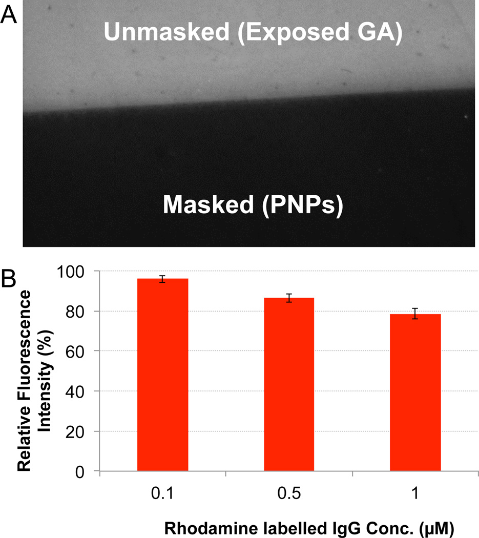
While continuous PNIPAM films have previously been used in surface blocking, a necessary first step was to assess the ability of PNP masks to function in this capacity. This was accomplished using flat silicon dioxide-on-silicon chips, first made protein reactive by aminosilane-gluteraldehyde chemistry followed by dipcoating 315 nm diameter PNIPAM particles on half of the substrate. The entire chip was then exposed to a solution of rhodamine labeled IgG (r-IgG) in a buffer containing physiologically relevant salt concentrations and rinsed. The fluorescence intensities of the PNIPAM-masked and unmasked portions of the chip were determined by epifluorescence microscopy, and were visibly higher on the unmasked regions of the substrate (Figure 4A). The relative fluorescence intensities of the masked regions were found to be 95% lower than the unmasked regions at 0.1 µM r-IgG (Figure 4B). Higher concentrations had decreased relative fluorescence intensities; however, the nanoparticle masks could still localize antibody effectively within the concentration range likely to be used for sensor functionalization.
Figure 4.
(A) Fluorescence image taken at l0x magnification (2 sec. exposure) of 0.1 µM. r-IgG incubated on a protein reactive (glutaraldehyde) substrate which was partially covered with a PNP mask. (B) Relative fluorescence intensities of the PNP masked surface for different concentrations of r-IgG was calculated by normalizing the ratio of the fluorescence intensities of the masked to the unmasked regions. Error bars for each condition are calculated from the standard deviations of the fluorescence intensities. See methods section for detailed formulae.
Nanoparticle assembly on 2D PhC structures
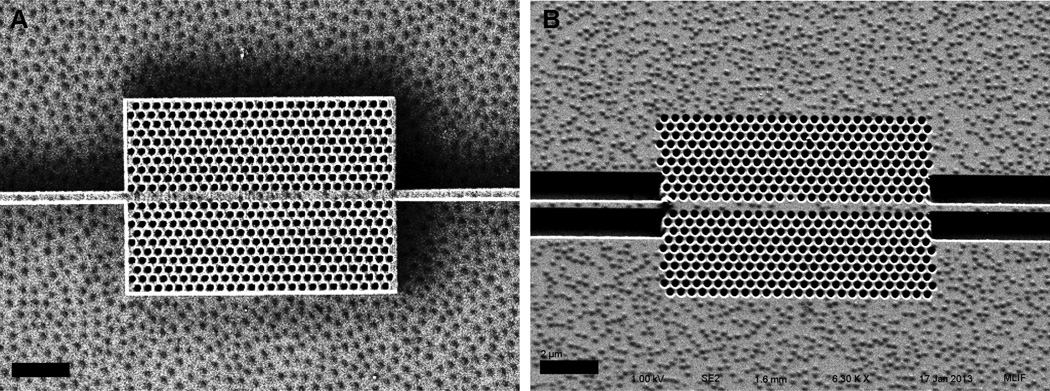
We hypothesized that assembling polymer nanoparticles (PNPs) with diameters larger than PhC wells would serve as an effective method for blocking most of the sensor’s surface, and allow for selective immobilization of capture molecules only in the sensitive regions of the PhC sensor. Indeed, when PNPs were deposited on a PhC chip via dip coating, they preferentially assembled around lithographed features as expected. Furthermore, the PNPs did not settle on top of the wells. This behavior was reproducible and consistent on both “extruded” and “embedded” versions of the sensor, fabricated via negative (Hydrogen silsesquioxane (HSQ)) and positive (Polymethylmethacrylate (PMMA)) tone resists respectively with e-beam lithography (Figure 5A and 5B). Consistent with prior studies of PNIPAM PNPs by SEM,36,37,38 dried particles imaged under the negligible humidity conditions of the SEM instrument appear to be widely spaced apart; as we describe above, hydrated particle films were effective at preventing antibody immobilization to these surfaces. While the particles employed in these experiments are too small for us to observe via optical microscopy, an analogously prepared film of larger particles assembled around nanoscale features and observed at ambient laboratory humidity shows that they indeed pack closely (supplementary information), consistent with the blocking ability of particle films.
Figure 5.
SEM images of HSQ (A), embedded PMMA (B) 2D PhCs dipcoated with PNIPAM PNPs. Scale bars represent 2 µm.
Enhanced limit of detection via topographically selective passivation
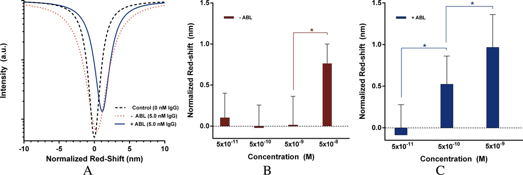
To test the effect of nanoparticle-mediated blocking of non-active portions of the sensor surface during functionalization, 2D PhC chips were functionalized with IgG (probe) and used to detect anti-IgG (target) at various concentrations. All protein deposition and binding experiments were conducted at physiologically relevant salt concentrations. The red-shift for each concentration was the difference in the wavelength of the minimum absorption before and after a chip was incubated at that particular anti-IgG concentration, subtracted from the red-shift of an identically functionalized control chip which was not exposed to anti-IgG. Two sets of experiments were run: one in which the chips were unmodified, and another in which the chips were dip-coated with PNIPAM particles prior to probe (IgG) functionalization. Each data point was tested with at least 3 devices. Normalizing the control shift value to zero allowed for a comparison of the relative shift (normalized red-shift) for chips with and without ABL exposed to 5 nM target (Figure 6A; note that imperfections in the chip fabrication process result in small differences in the quality factor, or “Q” for different 2D PhCs, and therefore the intensity of the defect absorption varies). Neither chip had statistically significant shifts from the controls with a target concentration of 50 pM. However, the antibody-localized (ABL) chip showed an increasing signal at all higher concentrations of target (Figure 6C), while the non-ABL chip required a 10-fold higher concentration than the ABL sensor to see a measurable signal (Figure 6B). The lowest detectable concentration of anti-IgG was found to be 0.5 nM with ABL, demonstrating that the LoD of our sensor was improved by at least one order of magnitude.
Figure 6.
Post-processed experimental peak shifts for two representative 2D-PhC sensors (A) which were incubated with capture antibody and set to zero red-shift (black dashed line); peak-shifts after incubation with 5 nM target without ABL (red dotted line) and with ABL (solid blue line). (B) and (C) Dose-response of a matched set of sensors without ABL (B, red bar) and with ABL (C, blue bar). Exposure of a second matched set of sensors with ABL to 50 nM target produced a similar red-shift (Supplementary Figure S2). Values that were statistically significant (unpaired 2-tailed student t-test, p-value < 0.05) were marked with an asterisk (*).Error bars were calculated by taking the square root of the sum of the control standard deviation squared plus the experimental standard deviation squared.
CONCLUSIONS
In order to improve the limit of detection of nanoscale biosensors, non-productive loss of target to inactive regions needs to be minimized. Precisely aligning top-down target delivery systems to nanoscale features on a substrate is challenging and requires expensive instrumentation. As an alternative, we developed a fast and inexpensive bottom-up technique based on dipcoating a monolayer of PNPs. We demonstrated that these PNPs assemble around topographically distinct features of 2D PhCs, leaving the active sensor area free for immobilization of capture antibodies. Consistent with FEM calculations, this provided over an order of magnitude improvement in the lowest limit of detection for the sensor. The 2D PhC sensor’s limit of detection depends strongly on the Q (quality) factor of the device as well as on the affinity of the capture molecule-analyte pair; for example, although the resolution of the laser currently employed in these experiments is 0.001 nm (and in the interest of completing experiments in a reasonable period of time scans are conducted with a resolution of 0.05 nm), the observable shift resolution is approximately 0.1 nm. As refinements in the sensor manufacturing process allow this to improve, the calculations also indicate that capture molecule localization will continue to provide a substantial performance enhancement. We anticipate that this strategy will work equally well with other nanoscale sensors, since most have topographical features distinguishing the active sensing area from the remainder of the device.
Supplementary Material
ACKNOWLEDGMENT
This work was supported by the National Institute of Health (R01A108077-01, to BLM, and T32AI049815-12, Training Grant in HIV Biology, to MAL). Device fabrication was performed in part at the Cornell NanoScale Science and Technology Facility (CNF), a member of the National Nanotechnology Infrastructure Network, which is supported by the National Science Foundation (ECS 03-35765). We thank Dr. Hsin-Yi Tsai for providing polymer nanoparticles used in preliminary experiments, and Dr. Alan R. Bleier for extensive help with electron beam nanolithography at CNF.
Footnotes
Supporting Information
Additional information as noted in text. This material is available free of charge via the Internet at http://pubs.acs.org.
Notes
The authors declare no competing financial interest.
REFERENCES
- 1.Fan X, White IM, Shopova SI, Zhu H, Suter JD, Sun Y. Anal. Chim. Acta. 2008;620:8–26. doi: 10.1016/j.aca.2008.05.022. [DOI] [PMC free article] [PubMed] [Google Scholar]
- 2.Chao C-Y, Guo LJ. Appl. Phys. Lett. 2003;83:1527–1529. [Google Scholar]
- 3.Armani AM, Kulkarni RP, Fraser SE, Flagan RC, Vahala KJ. Science. 2007;317:783–787. doi: 10.1126/science.1145002. [DOI] [PubMed] [Google Scholar]
- 4.Barrios CA, Gylfason KB, Sánchez B, Griol A, Sohlström H, Holgado M, Casquel R. Opt. Lett. 2007;32:3080–3082. doi: 10.1364/ol.32.003080. [DOI] [PubMed] [Google Scholar]
- 5.Heideman RG, Kooyman RPH, Greve J. Sens. Actuators, B. 1993;10:209–217. [Google Scholar]
- 6.Goddard NJ, Pollard-Knight D, Maule CH. Analyst. 1994;119:583–588. [Google Scholar]
- 7.Salamon Z, Tollin G. Biophys. J. 2001;80:1557–1567. doi: 10.1016/S0006-3495(01)76128-0. [DOI] [PMC free article] [PubMed] [Google Scholar]
- 8.Vollmer F, Braun D, Libchaber A, Khoshsima M, Teraoka I, Arnold S. Appl. Phys. Lett. 2002;80:4057–4059. [Google Scholar]
- 9.Krioukov E, Klunder DJW, Driessen A, Greve J, Otto C. Opt. Lett. 2002;27:1504–1506. doi: 10.1364/ol.27.001504. [DOI] [PubMed] [Google Scholar]
- 10.Sheehan PE, Whitman LJ. Nano Lett. 2005;5:803–807. doi: 10.1021/nl050298x. [DOI] [PubMed] [Google Scholar]
- 11.Lambeck PV. Meas. Sci. Technol. 2006;17:R93–R116. [Google Scholar]
- 12.Kusnezow W, Syagailo YV, Rüffer S, Baudenstiel N, Gauer C, Hoheisel JD, Wild D, Goychuk I. Mol. Cell. Proteomics. 2006;5:1681–1696. doi: 10.1074/mcp.T500035-MCP200. [DOI] [PubMed] [Google Scholar]
- 13.Sapsford KE, Liron Z, Shubin YS, Ligler FS. Anal. Chem. 2001;73:5518–5524. doi: 10.1021/ac015554e. [DOI] [PubMed] [Google Scholar]
- 14.Choi CJ, Belobraydich AR, Chan LL, Mathias PC, Cunningham BT. Anal. Biochem. 2010;405:1–10. doi: 10.1016/j.ab.2010.06.009. [DOI] [PubMed] [Google Scholar]
- 15.Ekins RP, Chu FW. Clin. Chem. 1991;37:1955–1967. [PubMed] [Google Scholar]
- 16.Ekins RP. Clin. Chem. 1998;44:2015–2030. [PubMed] [Google Scholar]
- 17.Parpia ZA, Kelso DM. Anal. Biochem. 2010;401:1–6. doi: 10.1016/j.ab.2009.03.050. [DOI] [PMC free article] [PubMed] [Google Scholar]
- 18.Taylor S, Smith S, Windle B, Guiseppi-Elie A. Nucleic Acids Res. 2003;31:e87. doi: 10.1093/nar/gng086. [DOI] [PMC free article] [PubMed] [Google Scholar]
- 19.McKendry R, Zhang J, Arntz Y, Strunz T, Hegner M, Lang HP, Baller MK, Certa U, Meyer E, Güntherodt H, Gerber C. Proc. Natl. Acad. Sci. U. S. A. 2002;99:9783–9788. doi: 10.1073/pnas.152330199. [DOI] [PMC free article] [PubMed] [Google Scholar]
- 20.Lee K, Kim E, Mirkin C, Wolinsky S. Nano Lett. 2004;4:1869–1872. [Google Scholar]
- 21.Feuz L, Jönsson P, Jonsson MP, Höök F. ACS Nano. 2010;4:2167–2177. doi: 10.1021/nn901457f. [DOI] [PubMed] [Google Scholar]
- 22.Pal S, Guillermain E, Sriram R, Miller BL, Fauchet PM. Biosens. Bioelectron. 2011;26:4024–4031. doi: 10.1016/j.bios.2011.03.024. [DOI] [PMC free article] [PubMed] [Google Scholar]
- 23.Schneider CA, Rasband WS, Eliceiri KW. Nat. Methods. 2012;9:671–675. doi: 10.1038/nmeth.2089. [DOI] [PMC free article] [PubMed] [Google Scholar]
- 24.Pal S, Yadav AR, Lifson MA, Baker JE, Fauchet PM, Miller BL. Biosens. Bioelectron. 2013;44:229–234. doi: 10.1016/j.bios.2013.01.004. [DOI] [PMC free article] [PubMed] [Google Scholar]
- 25.Pelton RH, Chibante P. Colloids Surf. 1986;20:247–256. [Google Scholar]
- 26.Andersson M, Maunu SL. J. Polym. Sci., Part B: Polym. Phys. 2006;44:3305–3314. [Google Scholar]
- 27.Blackburn WH, Lyon LA. Colloid Polym. Sci. 2008;286:563–569. doi: 10.1007/s00396-007-1805-7. [DOI] [PMC free article] [PubMed] [Google Scholar]
- 28.Kratz K, Hellweg T, Eimer W. Colloids Surf., A. 2000;170:137–149. [Google Scholar]
- 29.Hoare T, Pelton R. Macromolecules. 2004;37:2544–2550. [Google Scholar]
- 30.Karg M, Pastoriza-Santos I, Rodriguez-González B, Von Klitzing R, Wellert S, Hellweg T. Langmuir. 2008;24:6300–6306. doi: 10.1021/la702996p. [DOI] [PubMed] [Google Scholar]
- 31.Tsuji S, Kawaguchi H. Langmuir. 2005;21:8439–8442. doi: 10.1021/la050271t. [DOI] [PubMed] [Google Scholar]
- 32.Kawaguchi H, Fujimoto K, Mizuhara Y. Colloid Polym. Sci. 1992;270:53–57. [Google Scholar]
- 33.Huber DL, Manginell RP, Samara MA, Kim B-I, Bunker BC. Science. 2003;301:352–354. doi: 10.1126/science.1080759. [DOI] [PubMed] [Google Scholar]
- 34.Xue C, Yonet-Tanyeri N, Brouette N, Sferrazza M, Braun PV, Leckband DE. Langmuir. 2011;27:8810–8818. doi: 10.1021/la2001909. [DOI] [PMC free article] [PubMed] [Google Scholar]
- 35.Zhu X, Gu X, Zhang L, Kong X-Z. Nanoscale Res. Lett. 2012;7:519. doi: 10.1186/1556-276X-7-519. [DOI] [PMC free article] [PubMed] [Google Scholar]
- 36.Schmidt S, Motschmann H, Hellweg T, von Klitzing R. Polymer. 2008;49:749–756. [Google Scholar]
- 37.Horecha M, Senkovskyy V, Synytska A, Stamm M, Chervanyov AI, Kiriy A. Soft Matter. 2010;6:5980–5992. [Google Scholar]
- 38.Garcia-Salinas MJ, Donald AM. J. Coll. Interface Sci. 2010;342:629–635. doi: 10.1016/j.jcis.2009.10.064. [DOI] [PubMed] [Google Scholar]
Associated Data
This section collects any data citations, data availability statements, or supplementary materials included in this article.


