Abstract
In order to induce greater light absorption, nano-patterning is often applied to the metal-oxide buffer layer in inverted bulk-heterojunction(BHJ) solar cells. However, current homogeneity was significantly disturbed at the interface, leading to an efficiency that was not fully optimized. In this work, an additional PC61BM layer was inserted between the ZnO ripple and the photoactive layer to enhance the electron extraction. The insertion of additional PC61BM layer provided substantial advantages in the operation of inverted BHJ solar cells; specifically, it enhanced current homogeneity and lowered accumulation and trapping of photogenerated charges at the ZnO interface. Inclusion of the additional PC61BM layer led to effective quenching of electron–hole recombination by a reduction in the number of accumulated charges at the surface of ZnO ripples. This resulted in a 16% increase in the efficiency of inverted BHJ solar cells to 7.7%, compared to solar cells without the additional PC61BM layer.
Bulk heterojunction (BHJ) solar cells based on blends of conjugated polymers and soluble fullerene derivatives have generated strong interest in the field of renewable energy because of the potential they offer to lower manufacturing costs for large area, lightweight devices1,2,3. Since the first BHJ solar cell was reported in 19954,5, the power conversion efficiency (PCE) of BHJ solar cells has gradually improved due to the development of new materials and device architectures, recently reaching over 9% in single junction device6,7,8.
The inverted device architecture in particular has gained considerable attention in the research community because of its better device stability and advantages in processing over the conventional architecture9,10,11,12,13,14. In the inverted structure, since the polarity of charge collection is the opposite of that in the conventional architecture; the selection of an effective electron extraction/transportation buffer layer, which can effectively build-up the symmetry breaking, is the key component for high performance inverted solar cells15,16. Such an electron extraction/transportation buffer layer must be highly transparent, electrically conductive, and energetically well-matched to the lowest unoccupied molecular orbital (LUMO) level of the acceptor.
In order to induce greater light absorption in the photoactive layer, nano-patterning is often applied to the metal-oxide buffer layer, which functions as the electron extraction/transportation layer. Not only on metal-oxide buffer layer, plasticizer assistied soft embossing (PASE) structure have been applied on PEDOT:PSS hole extracting layer to improve solar cell performance17. For P3HT:PCBM solar cells based on PASE structured PEDOT:PSS layers the averaged overall power efficiency is improved by up to 18%. Many demonstrations of successful PCE enhancement through improved charge extraction and light absorption due to light scattered by the imprinted patterns have been reported to-date18,19,20,21. However, in most cases, the nano-patterning process is not simple, normally requiring the addition of complex fabrication steps.
Recently, we have demonstrated a simple method for spontaneous formation of nano-ripple structures on ZnO thin films fabricated using a sol-gel process; these nano-structured ZnO films were used as the hole-blocking, electron-transporting layer in inverted organic solar cells22,23,25,26. Although the ZnO ripple structure delivered some enhancement of light absorption via light scattering, current homogeneity was significantly disturbed at the interface between the photoactive and ZnO layers, leading to a PCE that was not fully optimized. This current inhomogeneity problem was resolved in our previous work by the application of an ultra-thin pure ZnO layer with atomic layer deposition (ALD)23,24. Although current technology allows the ALD processing on roll-to-roll process under near atmosphere pressure, ALD is still not a simple technique so far; rather, it requires complicates equipment and additional processing steps.
In this work, rather than deposition of an ultra-thin ZnO layer with ALD, we have applied an additional electron transporting layer of phenyl-C61-butyric acid methyl ester (PC61BM) by a simple spin-coating method. Inverted BHJ solar cells fabricated using poly(thienothiophene-co-benzodithiophenes)7-F20 (PTB7-F20) and phenyl-C71-butyric acid methyl ester (PC71BM) using the additional PC61BM layer exhibited a 16% increase in PCE (to 7.7%) compared to solar cells without the additional PC61BM layer (6.5%), which is consistent with previous literatures25,26. Current-sensing atomic force microscopy measurements and photoexcitation-assisted capacitance-voltage measurements were then used to investigate the exact role of the additional PC61BM layer on top of the ZnO ripple structure.
Results
Figure 1 shows a schematic illustration of the inverted solar cell structure as well as the chemical structures of the photoactive layer materials. After deposition of the solution-prepared ZnO on cleaned indium tin oxide (ITO)-coated glass by spin-coating under atmospheric conditions, a self-organized ripple nanostructure was introduced to enhance light absorption. Detailed procedures of the development of the ZnO nanostructures are described elsewhere22,23,27. Figure 2c shows the TEM cross-section image of the device with PC61BM layer. Since the ZnO and PCBM both showed dark phase in TEM image, it is somewhat difficult to distinguish. However, we thought that slight change of contrast from dark gray to light gray indicated PCBM layer. From the TEM image, we suspected that the thickness of PCBM layer is ca. 5 nm. This value was consistent with the result obtained from the comparison of total thickness between ITO/ZnO ripple/Active layer sample and ITO/ZnO ripple/PCBM/Active layer sample.
Figure 1.
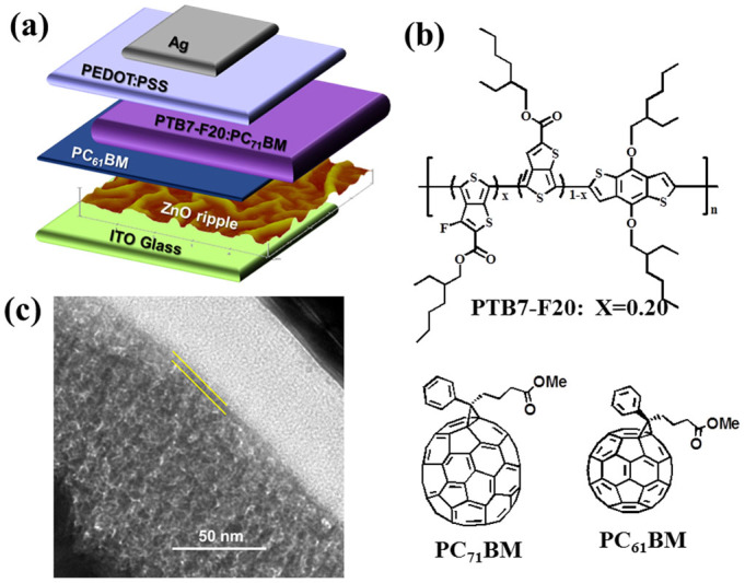
(a) Schematic illustration of an inverted solar cell structure and (b) chemical structures of the photoactive materials. (c) Cross section TEM image of the inverted BHJ solar cells with additional PC61BM layer.
Figure 2.
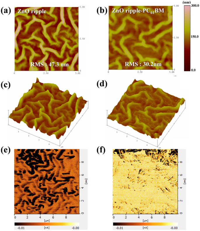
AFM height images of ZnO ripple structures (a) without and (b) with PC61BM. 3D AFM image of ZnO ripple structures (c) without and (d) with PC61BM. Current-sensing AFM images of ZnO ripple structures (e) without and (f) with PC61BM. Note that the current value in scale bar is individually normalized value to comparison.
Figure 2a and 2c show AFM images of ZnO ripple structures with a mean height of ~47 nm. Surface morphology images of ZnO ripples after spin-coating PC61BM on top is shown in Fig. 2b and 2d. Although the ripple nanostructures themselves were not significantly changed, the PC61BM coat was clearly distinguishable between crests. The root mean square (RMS) roughness was also reduced from 47.3 nm to 30.2 nm after the PC61BM spin-coating.
A more interesting effect of the additional PC61BM layer was observed in current-sensing AFM images shown in Fig. 2e and 2f. The current mapping image obtained from the ZnO ripple without PC61BM exhibits inhomogeneous current levels. The ripple nanostructure of ZnO can be seen quite clearly. However, in the current mapping image obtained from the ZnO layer with PC61BM, the ripple nanostructure shape largely disappeared, showing a relatively homogeneous current level across the image.
Such a current homogeneity has a critical effect on the BHJ solar cell performance. Figure 3a shows the current density (J)-voltage (V) characteristics of inverted PTB7-F20:PC71BM solar cells with and without PC61BM on the ZnO ripple. The solar cells fabricated without a PC61BM layer yielded a PCE of 6.475%, with a short circuit current density (Jsc) of 14.783 mA/cm2, an open circuit voltage (Voc) of 0.693 V, and a fill factor (FF) of 0.631. The solar cells including PC61BM, yielded a significantly enhanced PCE of 7.698%, with Jsc = 17.042 mA/cm2, Voc = 0.684 V, and FF = 0.660. Details related to the performance of the solar cells are listed in Table 1. A direct comparison of the J-V curves of the solar cells with and without the PC61BM layer clearly indicate that the enhanced PCE in the devices with PC61BM is largely based on an improvement of Jsc25,26. We attributed the increase in Jsc to the improved current homogeneity at the interface between the ZnO ripples and the photoactive layer. Addition of PC61BM layer on non-rippled ZnO layer also induced PCE enhancement. However, the PCE enhancement in device with non-rippled ZnO layer is originated from the Voc improvement (see Figure S5 in supporting information). Note that the PCE enhancement in devise with ZnO ripple was based on the improvement of Jsc. In non-rippled ZnO case, we suspected that there is a certain energy level modification of ZnO surface; maybe different band bending properties at the interface of non-rippled ZnO layer.
Figure 3.
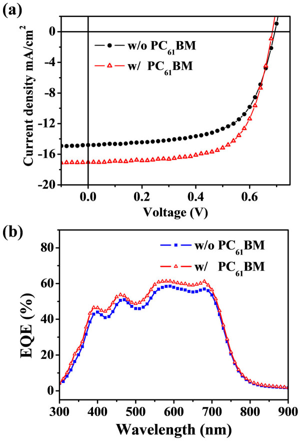
(a) J-V characteristics of inverted PTB7-F20:PC71BM solar cells with and without PC61BM on the ZnO ripple, (b) EQE spectra of the inverted PTB7-F20:PC71BM solar cells with and without the PC61BM layer.
Table 1. Photovoltaic performance of the inverted PTB7-F20:PC71BM solar cells with and without a PC61BM layer.
| PTB7-F20:PC71BM Inverted solar cells | PCE [%] | FF | Voc [V] | Jsc [mA/cm2] | Rs [Ω·cm2] |
|---|---|---|---|---|---|
| w/o PC61BM | 6.475 | 0.631 | 0.693 | 14.783 | 2.924 |
| w/PC61BM | 7.698 | 0.660 | 0.684 | 17.042 | 2.149 |
Figure 3b shows the external quantum efficiency (EQE) spectra for the inverted PTB7-F20:PC71BM solar cells with and without the PC61BM layer. The overall EQE spectrum of solar cell with PC61BM was slightly higher than that of the solar cell without it. Particularly, increase in EQE spectrum is occurred in entire wave range. It indicates that EQE enhancement is most likely due to the transport properties change, not because of optical property change by addition of PC61BM layer. The Jsc difference between the devices with and without PC61BM is consistent with the value derived from the EQE spectra.
In general, Jsc can also be strongly influenced by interfacial charge trapping at the metal oxide interface. Photoexcitation-assisted capacitance voltage (CV) spectroscopy was conducted to investigate the additional effect of the PC61BM layer on interfacial charge trapping and accumulation. Figure 4 shows the CV characteristics for devices both with and without the PC61BM layer at various photo-excitation intensities between 20 and 100 mW/cm2. In both sets of CV spectra, the effective capacitance increased with increasing photoexcitation intensity because effective capacitance under illumination is directly related to the density of photo generated charge28.
Figure 4.
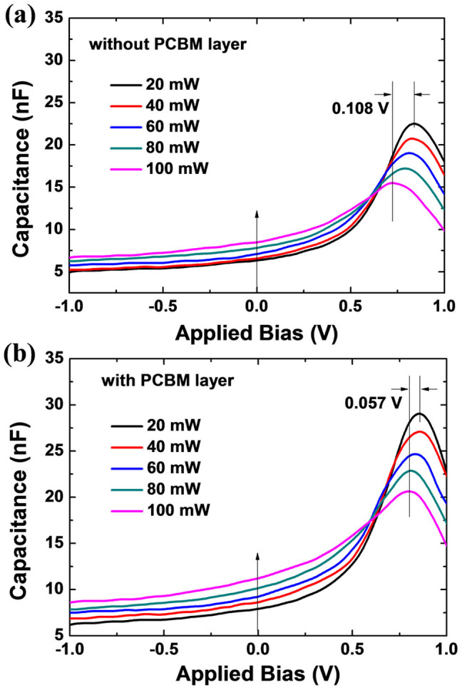
Photo-assisted capacitance-voltage characteristics at various photo-excitation intensities from 20 to 100 mW/cm2 (a) for the inverted PTB7-F20:PC71BM solar cells without a PC61BM layer and (b) for solar cells with a PC61BM layer.
Additionally, the voltage value at maximum capacitance (VC-max) shifted to a slightly lower voltage. VC-max generally corresponds to the voltage at which the charge carriers begin to inject, neutralizing the photo-generated charge, thereby decreasing the capacitance value (See supporting information, figure S5)29. Accordingly, VC-max should be reduced if the photo-generated charges accumulate at the metal oxide interface. In addition, the degree of VC-max shift will be proportional to the amount of accumulated charge. The observed VC-max shift was 0.108 V for the solar cells without a PC61BM layer (Figure 4a), while the solar cells with a PC61BM layer exhibited a much smaller VC-max shift of 0.057 V (Figure 4b). Therefore, comparison of the VC-max shifts between the solar cells with and without a PC61BM layer indicates that the solar cell with a PC61BM layer has a lesser accumulation of photo-generated charge at the interface. In other words, the additional PC61BM layer effectively prevented the trapping of charge at the surface of the ZnO ripples, thereby leading to better charge extraction.
In BHJ solar cells, non-geminate recombination via interfacial states, which exist at the donor-acceptor interface, is one of the dominant loss mechanisms30,31,32. Such non-geminate band-to-band recombination can also occur at the metal oxide-photoactive layer interface32. Impedance spectroscopy was used on inverted PTB7-F20:PC71BM solar cells both with and without a PC61BM layer on top of the ZnO ripple to clarify the dynamics of charge transport and recombination at the ZnO ripple surface. Figure 5 shows intensity-modulated photocurrent spectroscopy (IMPS) and intensity-modulated photovoltage spectroscopy (IMVS) results obtained under illumination with a narrow-band red LED light (635 nm). Note that 635 nm light is in the polymer absorption region. For the solar cells without a PC61BM layer, calculated transit time (τt, from IMPS) and recombination time (τr, from IMVS) were 64.4 and 120.9 μs, respectively29,31,33,34,35. For the solar cells with a PC61BM layer, τt and τr were calculated as 76.4 and 438.1 μs, respectively. Charge collection efficiencies (ηc) obtained via the relation ηc = 1 − (τt/τr), were 46.7% for solar cells without a PC61BM layer and 82.6% for solar cells with one36. These results are consistent with the results obtained from CV spectroscopy. Slower recombination time and enhanced charge collection efficiency in the solar cells with a PC61BM layer can be explained by the extra layer effectively covering trap sites and allowing less accumulation of photoexcited charges at the ZnO interface.
Figure 5. Nyquist plot of (a) IMPS and (b) IMPS results.
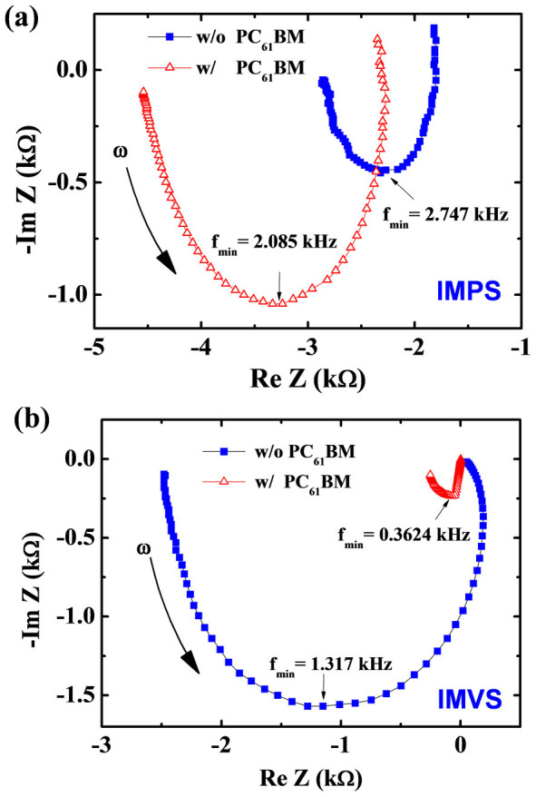
Narrow-band red LED light (635 nm) was used for the AC and DC components of the illumination. The mean transit time (τt) of photogenerated charges and recombination time (τr) were obtained at the frequency minimum in the Nyquist plot of IMVS and IMPS results.
In summary, we have demonstrated high performance inverted BHJ solar cells with PCEs enhanced by the insertion of an additional PC61BM layer between the self-organized, rippled ZnO and photoactive layers. Inverted BHJ solar cells including a PC61BM layer exhibited PCEs of 7.7%, nearly 16% higher than those of solar cells without an additional PC61BM layer. Insertion of an additional PC61BM layer provided substantial dynamic advantages in the operation of inverted BHJ solar cells. First, current-sensing AFM showed that the additional PC61BM layer clearly improved current homogeneity at the ZnO ripple-photoactive layer interface. Secondly, photo-excitation-assisted CV measurements indicated that the solar cells with a PC61BM layer accumulate and trap fewer photo-generated charges at the interface. IMPS and IMVS studies also clearly showed slower recombination time and enhanced charge collection efficiency in the solar cells with a PC61BM layer. We therefore concluded that the enhanced PCE in solar cells with a PC61BM layer was attributed to effective quenching of electron–hole recombination by reducing accumulated (or trapped) charges at the surface of the ZnO ripples.
Methods
Preparation of ZnO sol-gel
ZnO sol-gel solution (concentration of solution; 0.75 M) was prepared by dissolving zinc acetate [Zn(CH3COO)2.2H2O] (Aldrich, 99.9%) in 2-methoxyethanol (Aldrich, 99.8%) containing ethanolamine as a stabilizer. The solution was kept stirring for 2–3 h at 60°C using a magnetic stirrer to obtain a homogeneous solution.
Conductive AFM measurement
Conductive atomic force microscopy (C-AFM, Seiko E-Sweep) was conducted for evaluating the surface current flow in the films. For current images of the films, contact mode and tips with Pt/Ir were chosen.
Fabrication of inverted solar cells
Inverted solar cells studied in the present work consisted of a stack of ITO-coated glass\ZnO nano-ripple film with or without PC61BM layer\BHJ photoactive layer\PEDOT:PSS\Ag. ITO-coated glass substrates (4 Ω/□, 2.5 × 2.5 cm2) were first cleaned by ultrasonic agitation in detergent, deionized water, acetone, and isopropanol in sequence, followed by drying at 100°C in an oven for an hour and then UV ozone treatment for 30 min. 160 μl of ZnO solution was spin-coated on top of the pre-cleaned ITO glass at 2000 rpm for 40 sec. After coating, ZnO films were annealed at a constant heating rate of 22°C/min from room temperature up to 350°C to make a ZnO-ripple structure. The PC61BM was dissolved in chlorobenzene (CB) at a concentration of 1.0 wt%. The PC61BM solution was spin-cast on top of the ZnO-ripple film at a speed of 1000 rpm for 40 sec. The BHJ photoactive layers were spin cast at a speed of 1000 rpm for 40 sec in a N2-filled glove box from a solution of PTB7-F20:PC71BM (8 mg:12 mg) in CB with 3 v/v% 1,8-diiodooctane (DIO) that was first passed through a 0.20 μm polytetrafluoroethylene (PTFE) filter. To avoid washing out or mixing during the upper layer spin-coating, the lower PC61BM layer was covered with an orthogonal solvent, ethanol, by spin coating at 1500 rpm for 5 s, followed immediately by the upper layer of PTB7-F20:PC71BM. The coated films were annealed at 80°C for 10 min to evaporate residual solvent. After deposition of the photoactive layer, PEDOT:PSS (Clevios P VP AI 4083, Heraeus), diluted in isopropyl alcohol (in a 1:10 ratio) was spin-coated on top of the photoactive layer at 5000 rpm for 60 sec in a glovebox. It is worth emphasizing that no post annealing of PEDOT:PSS layers was performed. Finally, an Ag top electrode (100 nm) was deposited by thermal evaporation at 3 × 10⁻⁶ Torr using a shadow mask to form an active area of 0.38 cm2.
Characterization of solar cells
The current density–voltage (J–V) characteristics of the solar cell devices were measured using a PEC-L11 model 13 (Pecell Technologies Inc.) under simulated AM 1.5 illumination at an intensity of 100 mW/cm2. The intensity of sunlight illumination was calibrated using a standard Si-photodiode detector with a KG-5 filter. External quantum efficiency (EQE) spectra of each solar cell were measured using a solar cell spectral response/QE/IPCE measurement system (Newport co., Oriel IQE-200TM).
IMPS, IMVS and CV measurements
Photoexcitation-assisted CV measurements were carried out using HP4194 impedence analizer under illumination at various intensity of 20 ~ 100 mW/cm2. IMPS and IMVS were carried out using an impedance analyzer (IVIUM Tech., IviumStat). Both DC and AC components of the illumination were provided by the red emission LED (λ = 635 nm). The modulation depth of the AC component superimposed on the DC light was 10%. The light intensity was 0.86 mW/cm2, measured using a silicon photodiode. IMPS and IMVS were obtained under short-circuit and open-circuit conditions, respectively. The mean transit time (τt) and recombination time (τr) of photogenerated charges were obtained from the frequency minimum in the Nyquist plot of IMVS and IMPS results by setting τr,t = (2πfmin (IMVS, IMPS))−1.
Author Contributions
S.C., D.C.L. and Y.D.K. conceived this project. K.D.K., G.C. and B.Y.S. designed and fabricated the solar cells. S.C. and Y.S.K. collected the data of photo-assisted CV measurements and IMPS, IMVS measurements. J.H. and J.Y.L. performed the conductive AFM experiments. S.C. wrote the manuscript, and all other authors contributed to the edits of the manuscript.
Supplementary Material
Supporting information
Acknowledgments
This research was supported by a grant from KIMS. The portion of this research conducted at the University of Ulsan was supported by the Basic Science Research Program (NRF-2011-0009148, NRF-2013R1A2A2A01067741) and the Priority Research Centers Program (2009-0093818) through the National Research Foundation of Korea grant, funded by the Korean Government. Shinuk Cho and Kwang-Dae Kim contributed equally to this work.
References
- Thompson B. C. & Fréchet J. M. J. Polymer-fullerene composite solar cells. Angew. Chem. Int. Ed. 47, 58–77 (2008). [DOI] [PubMed] [Google Scholar]
- Brabec C. J. et al. Polymer–fullerene bulk-heterojunction solar cells. Adv. Mater. 22, 3839–3856 (2010). [DOI] [PubMed] [Google Scholar]
- Peet J., Senatore M. L., Heeger A. J. & Bazan G. C. The role of processing in the fabrication and optimization of plastic solar cells. Adv. Mater. 21, 1521–1527 (2009). [Google Scholar]
- Yu G., Hummelen J., Wudl F. & Heeger A. J. Polymer Photovoltaic Cells: Enhanced Efficiencies via a Network of Internal Donor-Acceptor Heterojunctions. Science 270, 1789–1791 (1995). [Google Scholar]
- Halls J. J. M. et al. Efficient photodiodes from interpenetrating polymer networks. Nature 376, 498–500 (1995). [Google Scholar]
- He Z. et al. Enhanced power-conversion efficiency in polymer solar cells using an inverted device structure. Nat. Photonics 6, 591–595 (2012). [Google Scholar]
- Cabanetos C. et al. Linear side chains in benzo[1,2-b:4,5-b']dithiophene-thieno[3,4-c]pyrrole-4,6-dione polymers direct self-assembly and solar cell performance. J. Am. Chem. Soc. 135, 4656–4659 (2013). [DOI] [PubMed] [Google Scholar]
- Dou L. et al. Tandem polymer solar cells featuring a spectrally matched low-bandgap polymer. Nat. Photonics 6, 180–185 (2012). [Google Scholar]
- Liao H.-H., Chen L.-M., Xu Z., Li G. & Yang Y. Highly efficient inverted polymer solar cell by low temperature annealing of Cs2CO3 interlayer. Appl. Phys. Lett. 92, 173303 (2008). [Google Scholar]
- White M. S., Olson D. C., Shaheen S. E., Kopidakis N. & Ginley D. S. Inverted bulk-heterojunction organic photovoltaic device using a solution-derived ZnO underlayer. Appl. Phys. Lett. 89, 143517 (2006). [Google Scholar]
- Waldauf C. et al. Highly efficient inverted organic photovoltaics using solution based titanium oxide as electron selective contact. Appl. Phys. Lett. 89, 233517 (2006). [Google Scholar]
- Jørgensen M. et al. Stability of polymer solar cells. Adv. Mater. 24, 580–612 (2012). [DOI] [PubMed] [Google Scholar]
- Shim W. H. et al. Multifunctional SWCNT-ZnO nanocomposites for enhancing performance and stability of organic solar cells. Adv. Mater. 23, 519–522 (2011). [DOI] [PubMed] [Google Scholar]
- Savva A. et al. The effect of organic and metal oxide interfacial layers on the performance of inverted organic photovoltaics. Adv. Energy Mat. 3, 391–398 (2013). [Google Scholar]
- Motiei L. et al. Self-propagating molecular assemblies as interlayers for efficient inverted bulk-heterojunction solar cells. J. Am. Chem. Soc. 132, 12528–12530 (2010). [DOI] [PubMed] [Google Scholar]
- Seo J. H., Kim H. & Cho S. Build-up of symmetry breaking using a titanium suboxide in bulk-heterojunction solar cells. Phys. Chem. Chem. Phys. 14, 4062–4065 (2012). [DOI] [PubMed] [Google Scholar]
- Meier R., Birkenstock C., Palumbiny C. M. & Müller-Buschbaum P. Efficiency-improved organic solar cells based on plasticizer assisted soft embossed PEDOT:PSS layers. Phys. Chem. Chem. Phys. 14, 15088–15098 (2012). [DOI] [PubMed] [Google Scholar]
- Emah J. B., Curry R. J. & Silva S. R. P. Low cost patterning of poly(3,4-ethylenedioxythiophene) poly(styrenesulfonate) films to increase organic photovoltaic device efficiency. Appl. Phys. Lett. 93, 103301 (2008). [Google Scholar]
- Wang D. H. et al. Effect of the ordered 2D-dot nano-patterned anode for polymer solar cells. Org. Electron. 11, 285–290 (2010). [Google Scholar]
- Wang D. H., Seifter J., Park J. H., Choi D.-G. & Heeger A. J. Efficiency increase in flexible bulk heterojunction solar cells with a nano-patterned indium zinc oxide anode. Adv. Energy Mater. 2, 1319–1322 (2012). [Google Scholar]
- Kang M.-G., Kim M.-S., Kim J. & Guo L. J. Organic solar cells using nanoimprinted transparent metal electrodes. Adv. Mater. 20, 4408–4413 (2008). [Google Scholar]
- Lim D. C. et al. Spontaneous formation of nanoripples on the surface of ZnO thin films as hole-blocking layer of inverted organic solar cells. Sol. Energy Mater. Sol. Cells 95, 3036–3040 (2011). [Google Scholar]
- Lim D. C. et al. Towards fabrication of high-performing organic photovoltaics: new donorpolymer, atomic layer deposited thin buffer layer and plasmonic effects. Energy Environ. Sci. 5, 9803–9807 (2012). [Google Scholar]
- Kim K.-D. et al. Surface modification of a ZnO electron-collecting layer using atomic layer deposition to fabricate high-performing inverted organic photovoltaics. ACS Appl. Mater. Interfaces 5, 8718–8723 (2013). [DOI] [PubMed] [Google Scholar]
- Hsieh C.-H. et al. Highly Efficient and Stable Inverted Polymer Solar Cells Integrated with a Cross-Linked Fullerene Material as an Interlayer, J. Am. Chem. Soc. 132, 4887–4893 (2010). [DOI] [PubMed] [Google Scholar]
- Cheng Y.-J., Hsieh C.-H., He Y., Hsu C.-S. & Li Y. Combination of Indene-C60 Bis-Adduct and Cross-Linked Fullerene Interlayer Leading to Highly Efficient Inverted Polymer Solar Cells. J. Am. Chem. Soc. 132, 17381–17383 (2010). [DOI] [PubMed] [Google Scholar]
- Park H.-Y., Lim D., Kim K.–D. & Jang S.–Y. Performance optimization of low-temperature-annealed solution-processable ZnO buffer layers for inverted polymer solar cells. J. Mater. Chem. A 1, 6327–6334 (2013). [Google Scholar]
- Boix P. P., Wienk M. M., Janssen R. A. J. & Garcia-Belmonte G. Open-circuit voltage limitation in low-bandgap diketopyrrolopyrrole-based polymer solar cells processed from different solvents. J. Phys. Chem. C 115, 15075–15080 (2011). [Google Scholar]
- Garcia-Belmonte G. et al. Charge carrier mobility and lifetime of organic bulk heterojunctions analyzed by impedance spectroscopy. Org. Electon. 9, 847–851 (2008). [Google Scholar]
- Cowan S. R., Street E. A., Cho S. & Heeger A. J. Transient photoconductivity in polymer bulk heterojunction solar cells: Competition between sweep-out and recombination. Phys. Rev. B 83, 035205 (2011). [Google Scholar]
- Byers J. C., Ballantyne S., Rodionov K., Mann A. & Semenikhin O. A. Mechanism of recombination losses in bulk heterojunction P3HT:PCBM solar cells studied using intensity modulated photocurrent spectroscopy. ACS Appl. Mater. Interfaces 3, 392–401 (2011). [DOI] [PubMed] [Google Scholar]
- Tachibana Y. et al. Organic conducting wire formation on a TiO2 nanocrystalline structure: towards long-lived charge separated systems. Chem. Commun., 4360–4362 (2009). [DOI] [PubMed] [Google Scholar]
- Fabregat-Samtiago F., Garcia-Belmonte G., Mora-Seró I. & Bisquert Characterization of nanostructured hybrid and organic solar cells by impedance spectroscopy. J. Phys. Chem. Chem. Phys. 13, 9083–9118 (2011). [DOI] [PubMed] [Google Scholar]
- Kavasoglu N., Kavasoglu A. S., Birgi O. & Oktik S. Intensity modulated short circuit current spectroscopy for solar cells. Sol. Energy Mater. Sol. Cells 95, 727–730 (2011). [Google Scholar]
- Bag M. & Narayan K. S. Universality in the intensity-modulated photocurrent in bulk-heterojunction polymer solar cells. Phys. Rev. B 82, 075308 (2010). [Google Scholar]
- Emin S., Yanagida M., Peng W. & Han L. Evaluation of carrier transport and recombinations in cadmium selenide quantum-dot-sensitized solar cells. Sol. Energy Mater. Sol. Cells 101, 5–10 (2012). [Google Scholar]
Associated Data
This section collects any data citations, data availability statements, or supplementary materials included in this article.
Supplementary Materials
Supporting information


