Abstract
Among various transdermal drug delivery (TDD) approaches, utilizing the microneedles (MNs) not only can penetrate the skin but also deliver the drug with reduced tissue damage, reduced pain, and no bleeding. However, the MNs with larger height are required to overcome the skin barrier for effective TDD. Unlike 2D patterning, etching polydimethyl siloxane (PDMS) micropillars for fabrication of 3D microstructures is presented. The PDMS micropillars were first constructed by casting PDMS on the computer numerical control-machined cylindrical microwells, which then went through etching process to obtain the MNs for subsequent fabrication of polymer MNs or high aspect ratio micropillars.
INTRODUCTION
In drug administration, transdermal drug delivery (TDD) offers several advantages over other conventional approaches such as preventing the drug from degradation in the gastrointestinal tract and first-pass effects of the liver associated with oral delivery, sustaining therapeutic drug level, permitting self-administration, improving patient compliance, being non-invasive, and long acting drug delivery. The main resistance of TDD originates from the protection function of the stratum corneum layer (about 20 μm) and viable epidermis layer (about 300 μm).1 In general, there are two strategies to overcome the diffusion resistance caused by the human skin. One is the chemical enhancement, which is the technique to change physical characteristics of lipid bilayer reversibly by using chemical compounds (sulphoxides, azones, pyrrolidones, alcohols, alkanols, etc.).2 The other is the physical enhancement, which includes iontophoresis, electroporation, ultrasound technique, and photoacoustic methods.3, 4, 5 Although the physical enhancement techniques are considered to be safer than the chemical enhancement techniques in terms of involvement of chemical compounds, additional equipment or setup is mandatory. To circumvent this issue, the silicon-based microneedle (MN) array with height at micron scale was introduced to provide an alternative for TDD.3 Unlike the conventional gauge needles, the MNs not only can penetrate the skin but also deliver the drug with reduced tissue damage, reduced pain, and no bleeding.6 The silicon-based MNs can be fabricated through patterning the metallic micromasks on the silicon wafer, followed by reactive ion etching (RIE) or wet etching by either isotropic etching with HNA (HF/Nitric/Acetic acid) solution or anisotropic etching with KOH etchant.7, 8 The height of the silicon-based MNs (or the replicated polymer MNs) is usually less than 400 μm due to the thickness of the silicon wafer (approximately 650 μm for 6 in. wafer). Although the total thickness of stratum corneum layer and the viable epidermis layer is around 350 μm, the height of the MNs for practical usage needs to be approximately 650 μm in order to compensate extra needle displacement resulted from folding of the skin around the MNs or partial penetration of MNs for effective drug administration.9 In order to meet the requirement of the height of the MNs, different strategies have been proposed. For example, Choi et al. used thick SU-8 photoresist and applied slanted exposure of UV light to prepare cone structure with height about 600 μm. They also combined back side exposure with RIE etching to fabricate SU-8 MNs array with high aspect ratio and shape adjustability.10 Park et al. obtained the cambered cavities on the glass substrate by HF etching, which serve as UV light refraction positions and the SU-8 photoresist was crosslinked to form a cone-like structure.11 The mechanical cutting, laser ablation, and electrical discharge machining were exploited to fabricate metallic MNs with desired height.12, 13, 14 The MNs fabricated by the abovementioned approaches can be used subsequently to obtain polydimethyl siloxane (PDMS) negative mold for fabrication of polymer MNs. However, these approaches, like silicon dry etching, still inevitably involve in some expensive equipment, or complicated procedure, and they are either energy or time consuming. Recently, drawing lithography was demonstrated to fabricate MNs with ultrahigh aspect ratio.15 Although this technique overcomes the height limitation of current subtractive-based lithography techniques, precise control of drawing and thermal curing of the viscoelastic thermosetting polymer is crucial for successful fabrication of MNs.
PDMS is a widely used material in micro/nanofabrication, especially soft lithography16 and microfluidic applications.17, 18, 19 While it is rarely found in the literature, PDMS itself can be directly used for 2D patterning through etching process such as making microchannels20 and microfeatures.21 In this study, a relatively fast, simple, reliable, and cost-effective method was proposed to fabricate MNs or high-aspect-ratio micropillars by etching PDMS micropillars. From the literature, most of the PDMS microneedles or micropillars were obtained through soft lithography by casting the PDMS onto the negative molds made of photoresist or silicon, which were produced by photolithographic process22, 23 or silicon dry etching.24 As to the polymer micropillars, the conventional practice is first to obtain the negative PDMS mold with a hole array, followed by casting the polymer solution25 or utilizing imprinting technique26 to produce the polymer micropillars. Different from the literature, our proposed technique is to directly etch the PDMS micropillars to form the microneedles or high-aspect ratio micropillars for subsequent fabrication of polymer microstructures. It was found that microneedles can be constructed through 3D etching of PDMS micropillars and the final height of the microneedles can be estimated by the initial height of the micropillars. Moreover, agitation of etchant solution plays an important role in determining the shape of the etched PDMS microneedles.
EXPERIMENTAL
Fabrication of PDMS microneedle array
The PDMS micropillar array was obtained by replicating the polymethyl methacrylate (PMMA) substrate with cylindrical microwell array, which was directly produced by the computer numerical control (CNC) machining (EGX-400, Roland). To minimize the surface roughness of the cylindrical microwells on the PMMA mold, the diamond coated milling cutter was selected. The diameter and depth of the microwells range from 200 to 400 μm and 300 to 800 μm, respectively. The pitch (center-to-center distance) of the microwells is 1 mm. The PDMS base and curing agent of 10:1 weight ratio were thoroughly mixed and degassed and the mixture was poured onto the PMMA substrate, followed by being placed in the 65 °C oven for 4 h. The fabricated 2 × 2 cm2 PDMS stamp with micropillar array was clamped to a cleaned glass slide and the assembly was hung on top of the beaker to allow the PDMS micropillars to immerse in the etchant composed of tetrabutylammonium fluoride (TBAF) and N-methylpyrrolidinone (NMP) at 1:6 volume ratio with the etching rate approximately 6 μm/min. After certain etching time, the etched PDMS micropillar array was removed from the etchant solution and rinsed by DI water, followed by being blown dry. As to agitation, a magnetic stirring bar was placed in the beaker, which was placed on top of the hot plate (PC-420D, Corning) with the rotation speed set to be 500 rpm.
Fabrication of polyvinyl pyrrolidone (PVP) microneedle array
To fabricate the polymer MNs, the double casting process was applied.27 The PDMS microneedle array was first treated with O2 plasma (Plasma cleaner, Harrick Plasma). The treated PDMS microneedles array and 1H,1H,2H,2H-perfluorooctyl tricholosilane (FOTS, Sigma Aldrich) were placed in the vacuum desiccator (50 mTorr) for 24 h to allow the FOTS to evaporate and modify the PDMS microneedle array, followed by casting PDMS. Once the PDMS is cured, the negative PDMS microneedle mold is peeled off for subsequent casting of polymer solution to obtain the polymer MNs. The polymer used in this study is PVP (MW = 360 000, Sigma Aldrich) and the polymer solution was prepared by dissolving PVP in the DI water at concentration of 10 wt. %.
RESULTS AND DISCUSSION
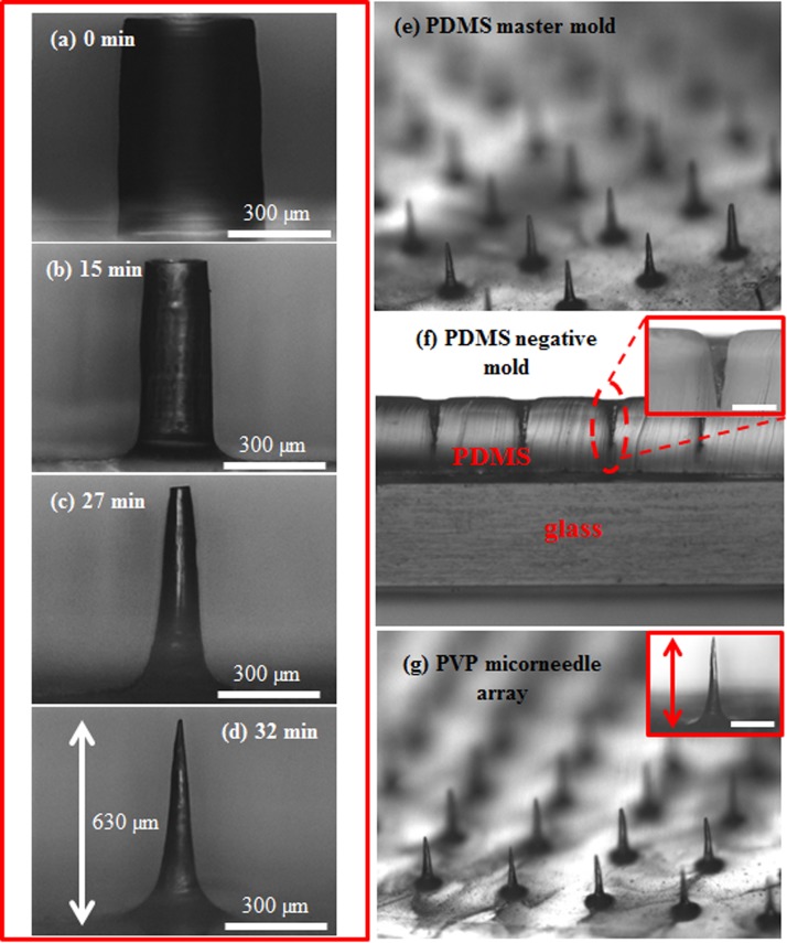
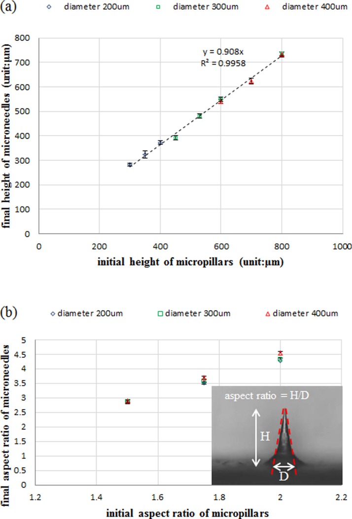
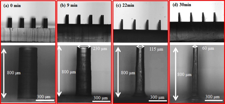
Figures 1a, 1b, 1c, 1d show the time lapsed images of etching PDMS micropillars without agitation. In the beginning, the PDMS micropillars were etched primarily in the radial direction and the diameter of the micropillars decreased uniformly from the top to the bottom as shown in Figure 1b. As the etching time increased, the top side of the micropillars was etched faster than the bottom, resulting in a conical-shape structure (Figure 1c). The difference in the local etching rates in the axial direction could be attributed to no agitation in the etchant solution where removal of the reaction byproduct near the bottom of the micropillars was less efficient, causing the decrease of the local etching rate. Further increasing the etching time leads to the formation of MNs as shown in Figure 1d. Because of the simplicity and robustness of this method, uniform MN array with height around 650 μm shown in Figure 1e can be generated readily and repetitively. Figure 1f shows the cross sectional view of PDMS negative mold peeled from the master mold. The modified master mold can be reused many times without any damage. The polymer MNs were obtained by casting 10 wt. % PVP solution on the negative PDMS mold as shown in Figure 1g. To test the polymer MNs for practical usage, the positive PDMS MNs mold with height around 600 μm and the PVP microneedles were repetitively produced in our lab. The average height of PVP microneedles is around 630 ± 20 μm, indicating robustness and reliability of the proposed method. Figure 2a shows that the final height of the PDMS MNs, which is approximately 90% of the initial height of the micropillars as seen from the trend line. Note that, since the PDMS MNs were obtained by etching PDMS micropillars till the sharp tips were formed and the height will decrease as the etching time is further prolonged, the final height of the MNs needs to be properly defined. In this study, the final height of the MNs is determined when the MNs with sharp tip are initially formed during the etching process. In addition, the aspect ratio of the MNs is positively proportional to that of the initial micropillars as shown in Figure 2b. The aspect ratio is defined as the height of the MNs divided by the base of the MNs, which is determined by the dashed lines shown in the inset of Figure 2b. Besides the above findings, agitation in the etchant solution also plays an important role in determining the etching profile. Figure 3 shows the time lapsed images of etching PDMS micropillars with agitation. In the beginning, the etching profile is similar to that without agitation. As the etching time increased, instead of forming the conical-shape structure, the etching profile remains the same and the micropillars with aspect ratio around 13 were obtained. It is hypothesized that the reaction byproduct generated near the bottom of the micropillars can be removed by action of agitation, which allows replenish of the etchant and the local etching rates can remain relatively constant. It is worthy of mentioning that the etching rate in the axial direction is almost negligible. The PVP micropillars with aspect ratio around 13 could also be produced as shown in Figure S1 in the supplementary material.28 Note that the micropillars with even larger aspect ratio (approximately 25) could be constructed (Figure S2 in the supplementary material28); however, bending of the micropillars occurs due to the lower mechanical strength of PDMS.
Figure 1.
(a) The initial micropillar with 400 μm in diameter and 700 μm in height. The optical images of PDMS micropillars at the etching time (b) 15, (c) 27, and (d) 32 min in the etching process without agitation. (e) The etched PDMS microneedle array. (f) The cross sectional view of the PDMS negative mold. (g) The PVP microneedle array. The scale bar in the insets of (f) and (g) is 300 μm.
Figure 2.
The relationship of (a) height and (b) aspect ratio between the initial PDMS micropillar and the etched PDMS MNs.
Figure 3.
(a) The initial PDMS micropillars with 300 μm in diameter and 800 μm in height. The optical images of PDMS micropillars at the etching time (b) 9, (c) 22, and (d) 30 min in the etching process with agitation (rotation speed of 500 rpm).
CONCLUSIONS
In this study, a relatively fast, simple, robust, and reliable method was demonstrated for fabrication of MNs and high aspect ratio micropillars. From programing CNC micromachining to obtaining the PDMS microneedle array, the turnaround time is less than 2 h and there is no photolithographic process or some expensive equipment involved for ICP-RIE dry etching. The final height and aspect ratio of the MNs can be determined by the dimensions of the initially produced PDMS micropillars. As to fabrication of the micropillars with high aspect ratio, agitation is required during the etching process, and the micropillars with aspect ratio around 13 were obtained.
ACKNOWLEDGMENTS
The authors are grateful for the financial support from the National Science Council (No. NSC 102-2221-E-006-192-MY2) and Chang Gung University (No. CMRPD1C0421) in Taiwan.
References
- Barry B. W., Eur. J. Pharm. Sci. 14(2 ), 101 (2001). 10.1016/S0928-0987(01)00167-1 [DOI] [PubMed] [Google Scholar]
- Williams A. C. and Barry B. W., Adv. Drug Deliv. Rev. 56(5 ), 603 (2004). 10.1016/j.addr.2003.10.025 [DOI] [PubMed] [Google Scholar]
- Henry S., McAllister D. V., Allen M. G., and Prausnitz M. R., J. Pharm. Sci. 87(8 ), 922 (1998). 10.1021/js980042+ [DOI] [PubMed] [Google Scholar]
- Pikal M. J., Adv. Drug Deliv. Rev. 46(1–3 ), 281 (2001). 10.1016/S0169-409X(00)00138-1 [DOI] [PubMed] [Google Scholar]
- Denet A. R., Vanbever R., and Preat V., Adv. Drug Deliv. Rev. 56(5 ), 659 (2004). 10.1016/j.addr.2003.10.027 [DOI] [PubMed] [Google Scholar]
- Folch i Folch A., Introduction to BioMEMS (CRC Press, Boca Raton, 2013), pp. xxxv. [Google Scholar]
- Wilke N., Mulcahy A., Ye S. R., and Morrissey A., Microelectron. J. 36(7 ), 650 (2005). 10.1016/j.mejo.2005.04.044 [DOI] [Google Scholar]
- Hamzah A. A., Abd Aziz N., Majlis B. Y., Yunas J., Dee C. F., and Bais B., J. Micromech. Microeng. 22(9 ), 095017 (2012) 10.1088/0960-1317/22/9/095017. [DOI] [Google Scholar]
- Martanto W., Moore J. S., Couse T., and Prausnitz M. R., J. Controlled Release 112(3 ), 357 (2006). 10.1016/j.jconrel.2006.02.017 [DOI] [PubMed] [Google Scholar]
- Choi S. O., Kim Y. C., Park J. H., Hutcheson J., Gill H. S., Yoon Y. K., Prausnitz M. R., and Allen M. G., Biomed. Microdevices 12(2 ), 263 (2010). 10.1007/s10544-009-9381-x [DOI] [PMC free article] [PubMed] [Google Scholar]
- Park J. H., Yoon Y. K., Choi S. O., Prausnitz M. R., and Allen M. G., IEEE Trans. Biomed. Eng. 54(5 ), 903 (2007). 10.1109/TBME.2006.889173 [DOI] [PubMed] [Google Scholar]
- Yuzhakov V. V., U.S. patent 07,658,728 (9 February 2010).
- Verbaan F. J., Bal S. M., van den Berg D. J., Dijksman J. A., van Hecke M., Verpoorten H., van den Berg A., Luttge R., and Bouwstra J. A., J. Controlled Release 128(1 ), 80 (2008). 10.1016/j.jconrel.2008.02.009 [DOI] [PubMed] [Google Scholar]
- Martanto W., Davis S. P., Holiday N. R., Wang J., Gill H. S., and Prausnitz M. R., Pharm. Res. 21(6 ), 947 (2004). 10.1023/B:PHAM.0000029282.44140.2e [DOI] [PubMed] [Google Scholar]
- Lee K., Lee H. C., Lee D.-S., and Jung H., Adv. Mater. 22(4 ), 483 (2010). 10.1002/adma.200902418 [DOI] [PubMed] [Google Scholar]
- Bowden N., Brittain S., Evans A. G., Hutchinson J. W., and Whitesides G. M., Nature 393(6681 ), 146 (1998). 10.1038/30193 [DOI] [Google Scholar]
- Duffy D. C., McDonald J. C., Schueller O. J. A., and Whitesides G. M., Anal. Chem. 70(23 ), 4974 (1998). 10.1021/ac980656z [DOI] [PubMed] [Google Scholar]
- McDonald J. C., Duffy D. C., Anderson J. R., Chiu D. T., Wu H. K., Schueller O. J. A., and Whitesides G. M., Electrophoresis 21(1 ), 27 (2000). [DOI] [PubMed] [Google Scholar]
- Folch A., Ayon A., Hurtado O., Schmidt M. A., and Toner M., J. Biomech. Eng. -Trans. ASME 121(1 ), 28 (1999). 10.1115/1.2798038 [DOI] [PubMed] [Google Scholar]
- Takayama S., Ostuni E., Qian X. P., McDonald J. C., Jiang X. Y., LeDuc P., Wu M. H., Ingber D. E., and Whitesides G. M., Adv. Mater. 13(8 ), 570 (2001). [DOI] [Google Scholar]
- Balakrisnan B., Patil S., and Smela E., J. Micromech. Microeng. 19(4 ), 047002 (2009) 10.1088/0960-1317/19/4/047002. [DOI] [Google Scholar]
- Ami Y., Tachikawa H., Takano N., and Miki N., J. Micro-Nanolithogr. MEMS MOEMS 10(1 ), 011503 (2011) 10.1117/1.3553393. [DOI] [Google Scholar]
- Nishinaka Y., Jun R., Setia Prihandana G., and Miki N., Jpn. J. Appl. Phys. 52(6 ), 06GL10 (2013) 10.7567/JJAP.52.06GL10. [DOI] [Google Scholar]
- Xin Z. and Yi Z., Sens. Actuators, A 125(2 ), 398 (2006). 10.1016/j.sna.2005.08.032 [DOI] [Google Scholar]
- Padeste C., Ozcelik H., Ziegler J., Schleunitz A., Bednarzik M., Yucel D., and Hasirci V., Microelectron. Eng. 88(8 ), 1836 (2011). 10.1016/j.mee.2010.11.051 [DOI] [Google Scholar]
- Shinohara H., Goto H., Kasahara T., and Mizuno J., Micromachines 4(2 ), 157 (2013). 10.3390/mi4020157 [DOI] [Google Scholar]
- Sniadecki N. J. and Chen C. S., in Methods in Cell Biology, edited by Wang Y.-L. and Discher Dennis E. (Academic Press, 2007), Vol. 83, p. 313. [DOI] [PubMed] [Google Scholar]
- See supplementary material at http://dx.doi.org/10.1063/1.4871038 for casting result of micropillar with aspect ratio of 13 and etched micropillar with aspect ratio of 25.


