Abstract
Nanoscale inorganic electronic synapses or synaptic devices, which are capable of emulating the functions of biological synapses of brain neuronal systems, are regarded as the basic building blocks for beyond-Von Neumann computing architecture, combining information storage and processing. Here, we demonstrate a Ag/AgInSbTe/Ag structure for chalcogenide memristor-based electronic synapses. The memristive characteristics with reproducible gradual resistance tuning are utilised to mimic the activity-dependent synaptic plasticity that serves as the basis of memory and learning. Bidirectional long-term Hebbian plasticity modulation is implemented by the coactivity of pre- and postsynaptic spikes, and the sign and degree are affected by assorted factors including the temporal difference, spike rate and voltage. Moreover, synaptic saturation is observed to be an adjustment of Hebbian rules to stabilise the growth of synaptic weights. Our results may contribute to the development of highly functional plastic electronic synapses and the further construction of next-generation parallel neuromorphic computing architecture.
The coming of the Big Data Era brings about an urgent demand for high-performance computing. However, the enhancement of computing capacity to cope with the complex real-time data environment is severely impeded by the von Neumann bottleneck, which refers to the limited data transfer rate between the central processing unit and the memory in the traditional computing architecture. The feasibility of combining the information storage and processing, eliminating the bottleneck, has been demonstrated in memristors or memristive devices using two paradigms: logic and neuromorphic computing, based on which new parallel computing architectures can be envisioned1,2,3,4. To implement error-free logic functioning, high uniformity of the resistive switching threshold voltage from cycle to cycle and from device to device is required2. However, the device variation cannot be reliably guaranteed for several reasons, for instance, drift during the fabrication process and the randomness of channel creation during the electroforming process. In contrast, its massive parallelism and high robustness against device variation and noise make the neuromorphic approach quite attractive5,6. To perform the human brain's cognitive functions utilising the neuromorphic approach, electronic devices that can mimic biological neurons and synapses are the crucial basic elements. In particular, memristor-based electronic synapses have drawn the bulk of research attention in recent years for two reasons. First, the intrinsic behaviour of memorising the flowing charges manifests as the self-adjustment of the device resistance, which is highly similar to the synaptic weight modification responding to the firing of pre- and postsynaptic neurons7. Second, the large number of transistor-based electronic synapses consume most of the power and area and hinder the further scaling of traditional very-large-scale integrated circuits (VLSI) neuromorphic chips. In view of many advantages, such as ultrafast synaptic function operation8, ultra-low power consumption9, sub-10-nm scalability10, over 1012 endurance11 and high connectivity of up to 4D architecture12, memristor-based neuromorphic chips may provide a promising approach to realize large scale brain-inspired computing.
Activity-dependent synaptic plasticity is fundamental for learning and memory in neuronal systems involving information processing and storage. Two opposite activity-dependent plasticity modifications have been biologically identified: long-term potentiation (LTP) and long-term depression (LTD)13,14. The former means a persistent increase in the synaptic transmission efficacy, whereas the latter is a decrease in the synaptic efficacy. In particular, the correlated activity of the presynaptic spike and postsynaptic firing, including the temporal relation14,15, the spike rate16,17,18, and the voltage18,19,20, may determine the polarity or degree of synaptic change.
Different synaptic functions such as spike-timing dependent plasticity (STDP) and memory consolidation have been demonstrated in various memristors or memristive devices, such as oxides6,21,22, chalcogenides8,23,24,25,26, ferroelectronics27,28, field effect transistors29,30 and carbon nanotubes31,32. In these implementations, two terminals of the device are always regarded as the pre- and postsynaptic sites when inputting the voltage spikes, and the device conductance or resistance represents the synaptic weight that reflects the connection strength of neurons. Biologically, the synaptic weight is analogue plastic, so that the continuous tuning of device conductance by voltage pulses is the key to successfully implementing synaptic functions. Please note that while STDP has been demonstrated in various memristive devices, the rate- and voltage-dependent modification of synaptic efficacy is rarely demonstrated.
In this work, a AgInSbTe (AIST)-based chalcogenide memristor, proposed in our previous study and showing reproducible gradual resistance tuning in both the bipolar and unipolar modes33, was utilised as an electronic synapse. The resistance could be tuned precisely by regulating the polarity, amplitude, width and number of the applied voltage pulses. By designing the applied pulse schemes, we reproduced in the AIST-based electronic synapse the activity-dependent synaptic plasticity of biological synapses, including four STDP forms, spike-rate dependent plasticity (SRDP) and synaptic voltage modulated plasticity. Moreover, synaptic saturation was also accomplished as an adjusting rule for the three type synaptic plastic learning rules.
Results
Memristance with gradual conductance tuning properties
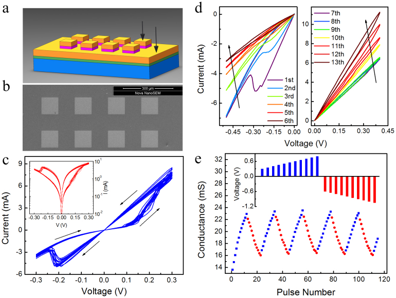
The presented Ag/AgInSbTe/Ag memristor that acts as an inorganic electronic synapse has a simple stacked structure with a 25-nm-AIST thin film (Fig. 1a, see Methods section for fabrication details). Such a simple stacked structure is convenient for building a large-scale synaptic matrix, which facilitates the massive fabrication and integration of neuromorphic circuits. Figure 1b shows a top view of the devices by scanning electron microscope (SEM). The surface uniformity, phase constitution and elemental composition of the AIST thin film were also studied using SEM, X-ray diffraction (XRD) and energy dispersive X-ray spectrum (EDX) (see supplementary Fig. S1–S3). The stable memristive characteristics as the basis of emulating synaptic functions were demonstrated. As shown in Fig. 1c, the typical current-voltage (I-V) relationship indicates a memristive behaviour featuring a conductance jump and drop at approximately 0.15 V and −0.2 V, respectively. The memristive mechanism is ascribed to the coexistence of the intrinsic space charge-limited conduction and the extrinsic electrochemical metallisation effect, which is further discussed in ref. 33. Figure 1d shows that the device conductance continuously increases or decreases due to the consecutive positive or negative voltage sweeps. This gradual conductance tuning property was also implemented in pulse stimulation mode (Fig. 1e), representing the synaptic weight modification in response to a potentiating or depressing stimulus. To achieve stable and repeatable conductance tuning, the pulse scheme was designed as shown in the inset of Fig. 1e. The potentiating pulse amplitudes increased from 0.3 V to 0.8 V with 50 mV steps. The depressing pulse amplitudes increased from −0.6 V to −1.1 V with 50 mV steps. All pulse widths were fixed at 5 μs. Sequences of identical positive and negative voltage pulses were able to gradually tune the conductance repeatably in over 20 different cells (see Supplementary Fig. S4). Notably, here the asymmetry of the potentiating and depressing pulse amplitudes, which may have resulted from the different barriers between the AIST film and the two electrodes due to the fabrication methods, plays a role in designing the pre- and post-synaptic spikes in the following synaptic plasticity experiments.
Figure 1. Memristive behaviours of Ag/AgInSbTe/Ag memristor.
(a) Schematic of the 100 × 100 μm2 Ag (100 nm)/AgInSbTe (25 nm)/Ag (100 nm) stack structures deposited on the Si/SiO2 substrate. (b) A scanning electron microscope image of the devices. (c) I-V characteristics showing bipolar memristive switches. Arrows indicate the voltage-sweep direction. Twenty cycles of operation are shown. (d) Gradual conductance modulation using voltage sweeping. The device conductance, which is equivalent to the synaptic weight, can be continuously increased or decreased by positive or negative voltage sweeps, respectively. (e) Repetitive gradual conductance modulation under pulse stimulation. The conductance variation range is approximately 7 mS. Upper inset: The pulse scheme. The positive and negative pulses correspond to the potentiating and depressing pulses, respectively.
Implementation of STDP
After the characterisation of the basic memristive properties of the AIST-based device, we proceed to demonstrate the activity-dependent plasticity in our electronic synapse. According to Hebb's theory, supported by a wealth of biological experiments, the synaptic efficacy is strengthened by concerted pre- and postsynaptic activity and is conversely weakened by non-coincidental neuronal firing14,34. In other words, the synaptic weight change Δw could be a function of Δt, where Δt represents the difference between the timing of the pre- and postsynaptic spikes. Figure 2 presents four ideal STDP functions used in computational models based on data measured experimentally from biological synapses14. The STDP forms vary due to different spikes or different type of synapses, excitatory or inhibitory. In some cases, the polarity of the synaptic weight change is determined by the temporal order of the pre- and postsynaptic spikes (Fig. 2a–b). In other cases, the polarity of the synaptic weight change depends only on the relative timing of the pre- and postsynaptic spikes, but not on their order (Fig. 2c–d). Generally, the synaptic modification reaches a maximum when the time difference is small because the activation of the pre- and postsynaptic neurons could be considered as synchronous. Exponential functions and Gaussian functions are used to quantify the STDP time window and are applied in computational neuroscience and neuromorphic hardware design.
Figure 2. Ideal STDP learning rules.
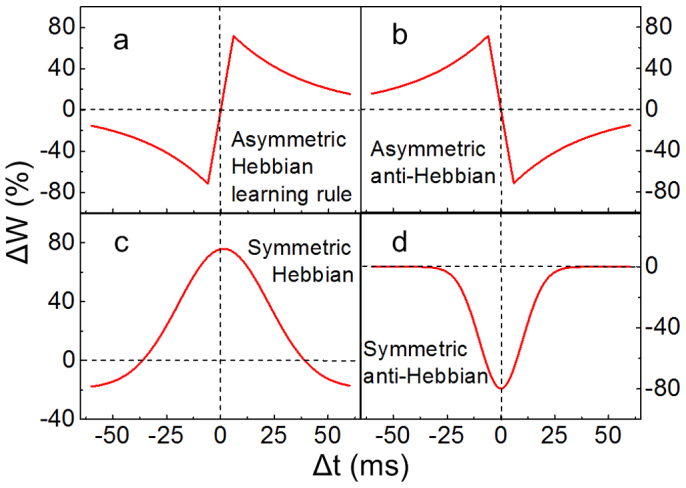
(a) Asymmetric Hebbian learning rule. (b) Asymmetric anti-Hebbian learning rule. (c) Symmetric Hebbian learning rule. (d) Symmetric anti-Hebbian learning rule.
We recently demonstrated these four different STDP forms in a Ge2Sb2Te5-based memristor employing a spike paring protocol, which is also adopted normally in biological synaptic experiments and in other electronic synapses8. In addition, the device conductance is defined as the synaptic weight (w) or synaptic efficacy, which biologically concerns the conductance of calcium ions in the ion channel, and the increase and decrease in synaptic weight represent LTP and LTD, respectively. Here, the same protocol and definition are followed when we design the pre- and postsynaptic spikes to operate the AIST-based synapse.
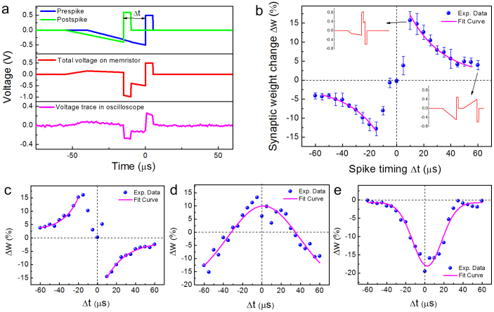
Consider, for instance, the most common asymmetric Hebbian STDP rule, followed by over 80% synapses in neocortical circuits: LTP when Δt > 0 and LTD when Δt < 0. The designed voltage pulse schemes are shown in Fig. 3a. There are threshold voltages, intrinsic to the memristive mechanism, that permit the modification of the synaptic weight and are different for potentiation and depression, as mentioned above. The pre- and postsynaptic spikes were applied to the bottom electrode and top electrode, respectively. The upper part of Fig. 3a shows a pair of pre- and postspikes with a 25 μs negative temporal difference. The total effective voltage on the memristor is Vpre(t) − Vpost(t), and the voltage trace is captured by an oscilloscope (lower part of Fig. 3a). By applying the paired spikes, the STDP learning rule was reproduced in our electronic synapse (Fig. 3b). Strengthening of the synapse occurred if the presynaptic spikes preceded the postsynaptic firing by no more than 70 μs, and presynaptic spikes that followed the postsynaptic spikes produced weakening of the synapse. The largest synaptic weight changes, approximately 15%, occurred when the time difference between the pre- and postsynaptic spikes was small, and there was a sharp transition from strengthening to weakening as the time difference passed through zero. This STDP time window could be fitted by
 |
where Δw is the percentage change in synaptic weight; Δt is the pre/post spike time difference; and A± and τ± are two parameters representing the scaling factor and the time constant of the exponential function, respectively15,35. The experimental data shown in Fig. 3b are well described by this function of Eq. (1) with A± = 24.33/−22.29 and τ± = 24.01/−22.84 μs. Fig. 3c–e show three other STDP forms appearing in biological neural networks, which could also be important supplements to the design of neuromorphic learning systems36 (for the details of pre/post spike pairs, see Supplementary Fig. S5). Note that the effect of synaptic modification could become more pronounced when trains of pre/post spikes are applied to the electronic synapse rather than the single pre/post pair in the above experiment, which is consistence with biological observations8,35. Moreover, by designing the pulse schemes, the time constant could be modulated in a wide temporal range, from the biological millisecond scale down to ultrafast nanoseconds8, providing flexibility for the peripheral neural circuit design and neuromorphic system design.
Figure 3. STDP implementation.
(a) Pulse schemes used to implement STDP. The upper part shows a pair of pre- and postspikes with a 25-μs negative temporal difference. The middle shows the total effective voltage on the memristor, which is Vpre(t) − Vpost(t). The lower part shows the voltage trace captured by an oscilloscope. (b) The asymmetric Hebbian learning STDP rule of memristor. The synaptic weight changes are plotted as a function of the time difference between the presynaptic spikes and postsynaptic spikes. The percentage changes are calculated with respect to the same initial value for all Δt, and the maximum change is approximately 15%. The error bars represent one standard deviation obtained from four measurements. The insets show two effective voltage pulses for Δt = 10 μs and 60 μs, respectively. (c–e) Demonstration of three other biological STDP forms in our memristor.
Implementation of SRDP
Next, we attempted to investigate another central rule of learning, the spike-rate dependent plasticity, which reflects the influence of the synaptic activation frequency on the long-lasting modification16,17.
All spikes are triangle voltage pulses with 5 μs rising time and 5 μs falling time. The voltage amplitudes are 1.2 V for the presynaptic spikes and 0.8 V for the postsynaptic spikes. The postsynaptic mean firing rate is tuned from 10 kHz to 83 kHz, and the presynaptic mean firing rate is fixed at 50 kHz. As shown in Fig. 4a, the efficacy of the synapse is decreased if the postsynaptic activity stays below a critical rate, fθ (50 kHz), and the weight is increased when the level of postsynaptic excitation exceeds the threshold. When the frequencies are 10, 50, 70 kHz, the synaptic weight changes are approximately −20%, 0%, 20%, respectively. The AIST-based device is a voltage-controlled memristor, and the total flux (time integral of voltage) flowing through the device determines the conductance change8,33, and at low postsynaptic frequencies (<50 kHz), the total flux flows from the bottom electrode to the top electrode, leading to long-term depression, whereas high frequencies (>50 kHz) induce long-term potentiation. Here, we used 50 pairs for each plot in Fig. 4a to achieve a relatively repetitive and stable magnitude, and 5 repeated measurements were carried out for statistics. Obviously, the magnitude of the potentiation and depression can be increased by increasing the pair number.
Figure 4. Implementation of SRDP in the inorganic memristor.
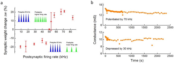
(a) Dependence of synaptic modification on the frequency of the postsynaptic firing rate induced by 50 repetitive stimulations. For postsynaptic firing rates below fθ (50 kHz), the synapse is depressed, while synaptic potentiation can be observed beyond fθ. The presynaptic rate is fixed at 50 kHz. (b) Changes in synaptic conductance following potentiation (upper) or depression (lower) stimulation. The synaptic efficacy remains stable over 2200 s, indicating a long-term modification. In the tests, all spikes are triangle voltage pulses with 5 μs rising time and 5 μs falling time. The voltage amplitudes are 1.2 V for the presynaptic spikes and 0.8 V for the postsynaptic spikes.
To determine whether the induction of potentiation and depression is long-term, the nonvolatile property of synaptic weight is also measured (Fig. 4b). After the 70 and 30 kHz postsynaptic stimulation, the conductance was changed to 15 and 10 mS, indicating that the electronic synapses were potentiated and depressed, respectively. The conductance remained at the same level over 2200 s, proving that the potentiation and depression are long-lasting modifications.
Synaptic voltage dependent plasticity modulation
Some biological experiments further suggest that the bidirectional learning rule could also be controlled by the postsynaptic voltage amplitude, that is, LTD and LTP can be induced by repetitive coincident pre- and postsynaptic stimulation with low and high postsynaptic voltage amplitudes19,20. The paring protocol then is employed to study the voltage-response function for induction of LTD and LTP. The postsynaptic voltage amplitude is tuned from 0.2 to 0.8 V, and the presynaptic voltage is fixed at 1.2 V. The pre- and post- spike frequencies are all 50 kHz. Figure 5a shows that a similar dependence to SRDP was demonstrated in the device. A threshold voltage amplitude (Vθ = 0.52 V) exists and divides the voltage-response function into two parts. LTD is induced when Vpost is more polarised than Vθ, and LTP is generated when Vpost is more depolarised than Vθ.
Figure 5. Bidirectional learning rule as a function of the postsynaptic potential.
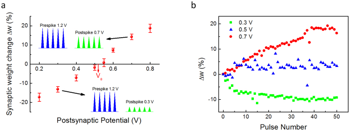
(a) In our memristor, the voltage-response function for the induction of LTD and LTP exhibits two parts: at a postsynaptic potential below Vθ, the synapse is depressed, whereas synaptic potentiation can be observed beyond Vθ. In this case, Vθ is approximately 0.52 V. (b) Dependence of synaptic modification on the pulse number. After approximately 40 coincident stimulations, the synaptic efficacy achieves stability, so 50 pairs of pre- and postsynaptic stimulations are used in each plot measurement of (a).
Synaptic saturation
The above experiments show that the synaptic weight can be modified by the cooperation of pre- and postsynaptic spikes, and the amount of variation relies on an effective flux, which is determined by the spike parameters, including the pulse amplitude, pulse width, pulse number and pulse interval. We further investigated the relationship between the amount of variation and the pulse parameters of the unidirectional square wave spikes applied to the device. Taking LTP as an example, Fig. 6a shows the dependence of the device conductance on the pulse amplitude and pulse number, with the pulse width and interval fixed at 5 μs and 1 s. Figure 6b shows the dependence of the device conductance on the pulse width and pulse number, with the pulse amplitude and interval fixed at 1 V and 1 s. When sustained spikes are applied to the device, the increase rate of the conductance decreases, and the conductance finally reaches an upper limit, which is higher with a larger pulse amplitude or width. In other words, the learning effect is most pronounced early in the exponential learning process, and the synaptic weight is only reinforced and saturated as the learning process continues, which is consistent with biological phenomena37. According to the Hebbian learning rule for LTP, synaptic activity increases the synaptic strength, and the increased synaptic strength leads to more activity and further modification. This positive feedback process may result in the uncontrolled growth of synaptic strengths and excessive neural firing. The synaptic saturation, i.e., the existence of a limited value of synaptic weight, is an inherent imposed constraint to modify the Hebbian rule. When saturation is reached, no further LTP or LTD can be induced, preventing new learning, even when the Hebbian induction criterion is met38. Physically, the saturation can be explained by the mechanism of the Ag/AgInSbTe/Ag memristor proposed in our previous work. During the application of continual spikes, multiple complete Ag filaments are formed, and the charge traps are filled, leading to a stable high-conductance state33.
Figure 6. Synaptic saturation.
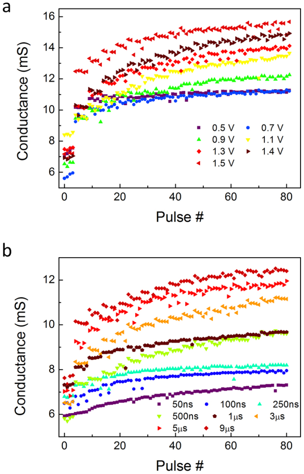
(a) Dependence of the device conductance on the pulse amplitude and pulse number. The pulse width and interval were 5 μs and 1 s, respectively. (b) Dependence of the device conductance on the pulse width and pulse number. The pulse amplitude and interval were 1 V and 1 s, respectively. Continual spikes push the plastic electronic synapse to its maximum strength, preventing further learning.
Discussion
Although synaptic plasticity is governed by a multifactor and multiform rule according to the type or location or function of the synapses, and the interaction between timing- and rate- and voltage-dependent processes is still under intense debate, independent STDP or SRDP function is widely utilised in computational and experimental neural networks to implement more complex cognitive functions, such as associative learning and pattern classification39,40,41.
We see the implementation of activity-dependent synaptic plasticity in an electronic synapse as a solid step toward constructing neuromorphic systems, but these results still call for additional research efforts on large-scale integration42. On the one hand, the performances of electronic synapses, such as power consumption and device scaling, need to be improved43. On the other hand, novel network architectures are urgently demanded44. The coordinated developments of above two aspects would breed the success of memristor-based neuromorphic computing.
In summary, in one Ag/AgInSbTe/Ag structure chalcogenide memristor-based electronic synapse, we have experimentally demonstrated the activity-dependent synaptic plasticity that is the basic phenomenon for learning in various neuronal systems. The spike-timing dependence of the four forms of plasticity were emulated, and long-term synaptic modification depends on the exact timing of the pre-and postsynaptic spikes. Spike-rate dependent changes and voltage-based modifications in synaptic plasticity were also performed, showing that LTP and LTP also depend on stimulation frequency and synaptic voltage. Moreover, synaptic saturation was observed in our electronic synapse, which is a crucial adjustment of Hebbian rules to stabilise the growth of synaptic weights. We believe that the demonstrated synaptic operation in this study, together with the booming development of sub-ns memristive devices with high density and low power consumption, will contribute to the construction of next-generation neuromorphic computing architecture that requires plastic electronic synapses.
Methods
Device fabrication
The electronic synaptic device consists of two 200-nm Ag electrodes with a thin AgInSbTe film with a thickness of 25 nm sandwiched between them. All layers were prepared by DC magnetron sputtering (JZCK-640S) at room temperature. The AIST film, which is the functional layer, was deposited with a 30 W sputtering power and a 0.5-Pa argon pressure. The bottom Ag electrode covers the whole SiO2/Si substrate. The pattern of the upper two layers was formed by photolithography (Karl Suss MJB3) with a dimension of approximately 100 × 100 μm2, followed by a AIST/Ag deposition and lift-off process. The schematic and a SEM (Nova NanoSEM 450) image of the device are shown in Figure 1a and 1b.
AIST film characterisation
For characterisation, 100-nm AIST films were deposited on quartz and silicon substrates and were characterised using X-ray diffraction (X′ Pert PRO Dy2198, Cu K-alpha radiation at a wavelength of 0.15418 nm, scan rate of 0.2°/s) and energy dispersive X-ray spectrum (Nova NanoSEM 450 scanning electron microscopy with EDX analysis). The XRD results for the as-deposited AIST indicate the films are in an amorphous state (supplementary Fig. S2). The EDX spectrum shows that the Ag:In:Sb:Te atom ratio is 4.51:5.89:58.52:31.08 (supplementary Fig. S3).
Device characterisation
A scanning electron microscope, working at room temperature, was used to take an image of the device array. The current-voltage (I-V) characteristics were measured using a four-probe system (Cascade S300) equipped with a semiconductor characterisation system (Keithley 4200-SCS) in the DC voltage sweep mode with a 100-mA current compliance. Pulse mode was utilised to provide pulse stimulus during the gradual conductance modulation, STDP and SRDP tests. The two terminals of the device were regarded as the pre- and post- synaptic locations and connected to two channels of the Keithley 4200, respectively. The various pulse schemes utilised in our test are programming generated by Keithley 4200, and captured with an oscilloscope (Agilent DSO5012A). During the electrical measurements, the positive bias was defined by the current flowing from the top electrode to the bottom one, and a small electrical pulse with low amplitude (10 mV) and short width (5 ms) was used as the read voltage. All measurements were performed at room temperature in air.
Author Contributions
Y.L., Y.Z. and X.M. conceived the idea, designed the experiments and analysed the data. J.Z. and Q.W. contributed to the device fabrication. L.X., H.T. and X.C. contributed to the film deposition and characterisation. Y.Z., Y.L., J.Z. and H.S. contributed to the memristance characterisation and demonstration of synaptic functions. Y.L. drafted the paper. X.M. supervised the project. All authors discussed the results and commented on the manuscript.
Supplementary Material
si_Activity-Dependent Synaptic Plasticity of a AgInSbTe-Based Electronic Synapse for Neuromorphic Systems
Acknowledgments
Financial supports from the National Natural Science Foundation of China (61376130), the Program of International S&T Cooperation (2010DFA11050), the National High-Tech R&D Program (863 Program) of China (2011AA010404), and the Fundamental Research Funds for Central Universities (HUST: 0118182046) are acknowledged. Thanks also to the facility support of the Center for Nanoscale Characterization and Devices of WNLO.
References
- Di Ventra M. & Pershin Y. V. The parallel approach. Nat. Phys. 9, 200–202 (2013). [Google Scholar]
- Borghetti J. et al. ‘Memristive’ switches enable ‘stateful’ logic operations via material implication. Nature 464, 873–876 (2010). [DOI] [PubMed] [Google Scholar]
- Jo S. H. et al. Nanoscale memristor device as synapse in neuromorphic systems. Nano Lett. 10, 1297–1301 (2010). [DOI] [PubMed] [Google Scholar]
- Yang J. J., Strukov D. B. & Stewart D. R. Memristive devices for computing. Nat. Nanotechnol. 8, 13–24 (2012). [DOI] [PubMed] [Google Scholar]
- Poon C.-S. & Zhou K. Neuromorphic silicon neurons and large-scale neural networks: challenges and opportunities. Front. Neurosci. 5, 108 (2011). [DOI] [PMC free article] [PubMed] [Google Scholar]
- Yu S. et al. A low energy oxide-based electronic synaptic device for neuromorphic visual systems with tolerance to device variation. Adv. Mater. 25, 1774–1779 (2013). [DOI] [PubMed] [Google Scholar]
- Linares-Barranco B. & Serrano-Gotarredona T. Memristance can explain spike-time-dependent-plasticity in neural synapses. Nature Precedings (2009). [Google Scholar]
- Li Y. et al. Ultrafast synaptic events in a chalcogenide memristor. Sci. Rep. 3, 1619 (2013). [DOI] [PMC free article] [PubMed] [Google Scholar]
- Wang X. P. et al. Highly compact 1T-1R architecture (4F2 footprint) involving fully CMOS compatible vertical GAA nano-pillar transistors and oxide-based RRAM cells exhibiting excellent NVM properties and ultra-low power operation. Electron Devices Meeting (IEDM), 2012 IEEE Int. 20.26.21–20.26.24 (2012). [Google Scholar]
- Govoreanu B. et al. 10 × 10 nm2 Hf/HfOx crossbar resistive RAM with excellent performance, reliability and low-energy operation. Electron Devices Meeting (IEDM), 2011 IEEE Int. 31.36.31–31.36.34 (2011). [Google Scholar]
- Lee M.-J. et al. A fast, high-endurance and scalable non-volatile memory device made from asymmetric Ta2O5-x/TaO2-x bilayer structures. Nat. Mater. 10, 625–630 (2011). [DOI] [PubMed] [Google Scholar]
- Strukov D. B. & Williams R. S. Four-dimensional address topology for circuits with stacked multilayer crossbar arrays. Proc. Natl. Acad. Sci. USA 106, 20155–20158 (2009). [DOI] [PMC free article] [PubMed] [Google Scholar]
- Feldman D. E. The spike-timing dependence of plasticity. Neuron 75, 556–571 (2012). [DOI] [PMC free article] [PubMed] [Google Scholar]
- Abbott L. F. & Nelson S. B. Synaptic plasticity: taming the beast. Nat. Neurosci. 3, 1178–1183 (2000). [DOI] [PubMed] [Google Scholar]
- Froemke R. C., Debanne D. & Bi G.-Q. Temporal modulation of spike-timing-dependent plasticity. Front. Syn. Neurosci. 2, 19 (2010). [DOI] [PMC free article] [PubMed] [Google Scholar]
- Xu C., Zhao M.-X., Poo M.-M. & Zhang X.-H. GABAB receptor activation mediates frequency-dependent plasticity of developing GABAergic synapses. Nat. Neurosci. 11, 1410–1418 (2008). [DOI] [PubMed] [Google Scholar]
- Kumar A. & Mehta M. R. Frequency-dependent changes in NMDAR-dependent synaptic plasticity. Front. Comput. Neurosci. 5, 38 (2011). [DOI] [PMC free article] [PubMed] [Google Scholar]
- Gerstner W. & Kistler W. M. Spiking neuron models: single neurons, populations, plasticity. (Cambridge Univ. Press, Cambridge, 2002). [Google Scholar]
- Ngezahayo A., Schachner M. & Artola A. Synaptic activity modulates the induction of bidirectional synaptic changes in adult mouse hippocampus. J. Neurosci. 20, 2451–2458 (2000). [DOI] [PMC free article] [PubMed] [Google Scholar]
- Clopath C., Büsing L., Vasilaki E. & Gerstner W. Connectivity reflects coding: a model of voltage-based STDP with homeostasis. Nat. Neurosci. 13, 344–352 (2010). [DOI] [PubMed] [Google Scholar]
- Chang T., Jo S. H. & Lu W. Short-term memory to long-term memory transition in a nanoscale memristor. ACS nano 5, 7669–7676 (2011). [DOI] [PubMed] [Google Scholar]
- Yang R. et al. On-demand nanodevice with electrical and neuromorphic multifunction realized by local ion migration. ACS nano 6, 9515–9521 (2012). [DOI] [PubMed] [Google Scholar]
- Kuzum D., Jeyasingh R. G. D., Lee B. & Wong H.-S. P. Nanoelectronic programmable synapses based on phase change materials for brain-inspired computing. Nano Lett. 12, 2179–2186 (2012). [DOI] [PubMed] [Google Scholar]
- Suri M. et al. Physical aspects of low power synapses based on phase change memory devices. J. Appl. Phys. 112, 054904 (2012). [Google Scholar]
- Ohno T. et al. Short-term plasticity and long-term potentiation mimicked in single inorganic synapses. Nat. Mater. 10, 591–595 (2011). [DOI] [PubMed] [Google Scholar]
- Nayak A. et al. Controlling the synaptic plasticity of a Cu2S gap-type atomic switch. Adv. Funct. Mater. 17, 3606–3613 (2012). [Google Scholar]
- Krzysteczko P., Münchenberger J., Schäfers M., Reiss G. & Thomas A. The memristive magnetic tunnel junction as a nanoscopic synapse-neuron system. Adv. Mater. 24, 762–766 (2012). [DOI] [PubMed] [Google Scholar]
- Chanthbouala A. et al. A ferroelectric memristor. Nat. Mater. 11, 860–864 (2012). [DOI] [PubMed] [Google Scholar]
- Alibart F. et al. An organic nanoparticle transistor behaving as a biological spiking synapse. Adv. Funct. Mater. 20, 330–337 (2010). [Google Scholar]
- Lai Q. et al. Ionic/electronic hybrid materials integrated in a synaptic transistor with signal processing and learning functions. Adv. Mater. 22, 2448–2453 (2010). [DOI] [PubMed] [Google Scholar]
- Zhao W. et al. Nanotube devices based crossbar architecture: toward neuromorphic computing. Nanotechnology 21, 175202 (2010). [DOI] [PubMed] [Google Scholar]
- Shen A. M. et al. Analog neuromorphic module based on carbon nanotube synapses. ACS nano 7, 6117–6122 (2013). [DOI] [PubMed] [Google Scholar]
- Zhang J. et al. AgInSbTe memristor with gradual resistance tuning. Appl. Phys. Lett. 102, 183513 (2013). [Google Scholar]
- Caporale N. & Dan Y. Spike timing-dependent plasticity: a Hebbian learning rule. Annu. Rev. Neurosci. 31, 25–46 (2008). [DOI] [PubMed] [Google Scholar]
- Froemke R. C. & Dan Y. Spike-timing-dependent synaptic modification induced by natural spike trains. Nature 416, 433–438 (2002). [DOI] [PubMed] [Google Scholar]
- Serrano-Gotarredona T., Masquelier T., Prodromakis T., Indiveri G. & Linares-Barranco B. STDP and STDP variations with memristors for spiking neuromorphic learning systems. Front. Neurosci. 7, 2 (2013). [DOI] [PMC free article] [PubMed] [Google Scholar]
- Dayan P. & Abbott L. F. Theoretical neuroscience: Computational and mathematical modeling of neural systems. (MIT Press, Cambridge, Massachusetts, 2001). [Google Scholar]
- Martin S., Grimwood P. & Morris R. Synaptic plasticity and memory: an evaluation of the hypothesis. Annu. Rev. Neurosci. 23, 649–711 (2000). [DOI] [PubMed] [Google Scholar]
- Ziegler M. et al. An electronic version of Pavlov's dog. Adv. Funct. Mater. 22, 2744–2749 (2012). [Google Scholar]
- Bichler O. et al. Pavlov's dog associative learning demonstrated on synaptic-like organic transistors. Neural Comput. 25, 549–566 (2012). [DOI] [PubMed] [Google Scholar]
- Alibart F., Zamanidoost E. & Strukov D. B. Pattern classification by memristive crossbar circuits using ex situ and in situ training. Nat. Commun. 4, 2072 (2013). [DOI] [PubMed] [Google Scholar]
- Jeong D. S., Kim I., Ziegler M. & Kohlstedt H. Towards artificial neurons and synapses: a materials point of view. RSC Adv. 3, 3169 (2013). [Google Scholar]
- Kuzum D., Yu S. & Wong H.-S. P. Synaptic electronics: materials, devices and applications. Nanotechnology 24, 382001 (2013). [DOI] [PubMed] [Google Scholar]
- Indiveri G., Linares-Barranco B., Legenstein R., Deligeorgis G. & Prodromakis T. Integration of nanoscale memristor synapses in neuromorphic computing architectures. Nanotechnology 24, 384010 (2013). [DOI] [PubMed] [Google Scholar]
Associated Data
This section collects any data citations, data availability statements, or supplementary materials included in this article.
Supplementary Materials
si_Activity-Dependent Synaptic Plasticity of a AgInSbTe-Based Electronic Synapse for Neuromorphic Systems


