Abstract
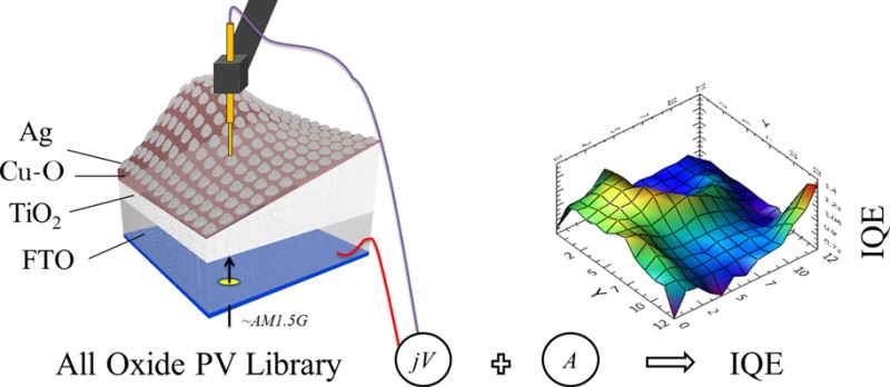
All-oxide-based photovoltaics (PVs) encompass the potential for extremely low cost solar cells, provided they can obtain an order of magnitude improvement in their power conversion efficiencies. To achieve this goal, we perform a combinatorial materials study of metal oxide based light absorbers, charge transporters, junctions between them, and PV devices. Here we report the development of a combinatorial internal quantum efficiency (IQE) method. IQE measures the efficiency associated with the charge separation and collection processes, and thus is a proxy for PV activity of materials once placed into devices, discarding optical properties that cause uncontrolled light harvesting. The IQE is supported by high-throughput techniques for bandgap fitting, composition analysis, and thickness mapping, which are also crucial parameters for the combinatorial investigation cycle of photovoltaics. As a model system we use a library of 169 solar cells with a varying thickness of sprayed titanium dioxide (TiO2) as the window layer, and covarying thickness and composition of binary compounds of copper oxides (Cu–O) as the light absorber, fabricated by Pulsed Laser Deposition (PLD). The analysis on the combinatorial devices shows the correlation between compositions and bandgap, and their effect on PV activity within several device configurations. The analysis suggests that the presence of Cu4O3 plays a significant role in the PV activity of binary Cu–O compounds.
Keywords: heterojunction, thin films, continuous compositional spread, photophysics, nanotechnology, photochemistry
1. Introduction
The ability of photovoltaic (PV) technologies to fulfill the global demand for energy can be addressed by the following criteria: (a) that they are cost efficient, that is, cheap to produce and to maintain, have relatively high solar power conversion efficiency, and are stable during their lifetime, and (b) that they are environmentally friendly in terms of toxicity and carbon footprint. Because of the past decade’s demand for renewable energies, the PV market has shown great growth, facilitated by cost reductions,1−5 and the emergence of novel and promising technologies.6−11 Yet a significant gap between the ultimate PV platform, that addresses the above criteria, and the currently available systems, calls for new PV technologies. Solar cells based on metal oxides have hardly been studied, compared to other technologies, though photovoltaic effects surely exist in this type of semiconductor.12 The abundance of metal oxides, combined with their low toxicity, ease of processing, low energy of processing, and stability can be considered ultimately as the basis for excellent photovoltaic modules.2 Nevertheless, a metal oxide based solar cell that has high power conversion efficiency has not yet been realized.
Figure 1 shows a schematic example of an energy band diagram and a basic working principle of a heterojunction all-oxide PV cell, formed between a layer of TiO2, which is a wide bandgap semitransparent n-Type semiconductor, a layer of Cu–O that serves as a light absorbing layer, silver as the back contact and Fluorine doped Tin Oxide (FTO) as the front contact. Alternative absorbers can be based on Co–O or Fe–O, whereas ZnO, WO3 and NiO are examples of alternative window layers. Doping, alloying or phase mixing between each of these oxides (wide or narrow bandgap), or with a nonconducting wide bandgap metal oxide (e.g., MgO, ZrO), or with metals, can provide novel combinatorial materials that replace the layers shown in Figure 1. In this work we use the configuration shown in Figure 1 as a model system, since most of the cells in this library showed some photovoltaic behavior. Common binary oxides of copper, with Cu–O as the abbreviation, are Cu2O (cuprite or cuprous oxide), CuO (tenorite or cupric oxide) and Cu4O3 (paramelaconite). Schottky junctions,15−17 homojunctions,18−21 heterojunctions,12,22−27 and nanocomposite heterojunctions28−34 based on Cu2O were studied two decades ago and lately started to regain interest. Power conversion efficiencies of ∼4–5% were reported for heterojunctions of Cu2O and ZnO or Ga2O3.25,26,35 To our knowledge, solar cells based on CuO and Cu4O3 have not achieved noticeable photovoltaic performance and have been less studied despite their bandgap being more appropriate for the sun’s spectrum.36 There are some inconsistencies in the measured and calculated bandgaps for these oxides; mainly there are ambiguities about the exact value of the bandgap for pure CuO and to what extent it is a direct or indirect transition.37−40 Overall, it has been said that the bandgap of Cu–O compounds can be tuned between 2.1 and 1.4 eV.41,42 In a recent perspective article, we provide more information and a literature survey about the advantages, limitations, and challenges of all-oxide solar cells, that is, photovoltaic devices based almost entirely on metal oxides.14 We have chosen to confront this challenge using combinatorial material science for the discovery of novel metal oxide absorbers, charge transporting materials, and selective contacts. Generally, combinatorial and high throughput approaches were proven to be useful in the research of medicine, active compounds, materials, and devices.43−56 More relevant are combinatorial studies for the development of photovoltaics, such as bulk heterojunction solar cells,57−60 thin film solar cells,49,61−64 and related optoelectronic and photoelectrochemical devices.44,47,65−70
Figure 1.
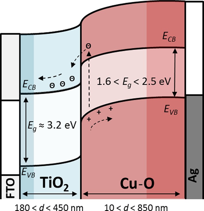
Schematic energy band diagram of a heterojunction PV cell, approximated to form under short circuit conditions. The combinatorial library in this work varies in the thickness, d, of TiO2 and covaries in the thickness, the level of oxidation, and hence the bandgap (Eg) of the copper oxide layer (Cu–O). The level of band bending, the position of the valence band edge (Evb), and the conduction band edge (Ecb) of the Cu–O with respect to the TiO2 are approximations, more information can be found in refs (13 and 14).
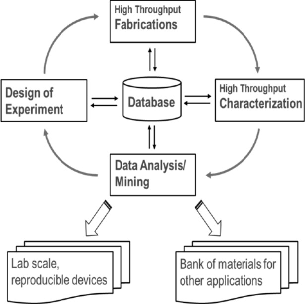
Figure 2 shows the combinatorial development cycle adopted for the all-oxide PV research.50,51 To date, we have accumulated in our database information on hundreds of device libraries and subsets of device libraries. The devices were constructed from various metal oxides and/or combinatorial metal oxides that underwent various treatments. The subsequent libraries have gone through the combinatorial cycle of fabrication, characterization, and analysis steps mentioned in the caption of Figure 2. The design of experiment, the choice of materials, and the supporting techniques used here are based on information from these libraries. Ultimately, this work is concerned with one major photovoltaic device library, consisting of 169 cells, and two additional subset libraries that mirror the components of the major library. The subset libraries are absorber only on glass and sprayed TiO2 only on TCO.
Figure 2.
Combinatorial development cycle for all-oxide PV. High throughput fabrication is performed using the following: spray pyrolysis, pulsed laser deposition, and RF sputtering. For high throughput characterization, (a) thickness measurements with scanning profilometer, optical analysis, and combined focused ion beam (FIB) cross sections analyzed under scanning electron microscopy (SEM). (b) For optical measurements, scanning UV–vis–NIR spectroscopy of total transmission, total reflection, and specular reflection. (c) For device performance, scanning current–voltage measurements under solar simulation. (d) For composition: Raman mapping combined with bandgap analysis. Data analysis: (a) algorithms for current–voltage curves analysis to derive photovoltaic parameters, (b) absorptance calculations, (c) semiautomatic bandgap fitting using thickness and absorptance, and (d) internal quantum efficiency calculations based on absorptance and current–voltage analysis.
The absorber layer in this work is deposited using the pulsed laser deposition technique (PLD). This technique allows for a continuous compositional spread, and hence can enable high throughput detailed material investigations of alloying, doping, thickness gradient, thermal treatment, and controlled atmosphere effects. PLD uses very high intensity pulses of UV laser to deposit subatomic layers from a target of pure material onto a substrate. The thickness and deposition energetics vary as function of position on the substrate, thus several values are convoluted within the composition. Heat treatments, specific atmospheric conditions, and deposition via aperture can be used in order to achieve homogeneous depositions.71−74 In this work, we deposit a thickness-composition gradient from a CuO target under room temperature, with no heat treatment and under low pressure of oxygen. Combining data from Raman measurements and bandgap analysis, we find that the resulting materials are a mixture of the aforementioned oxides of copper, changing as a function of distance from the center of deposition. These two covarying parameters, together with the thickness gradient of the underlying TiO2 layer, provide us with a very large diversity of cells in the library.
The experiment here demonstrates the importance of the Internal Quantum Efficiency technique in the combinatorial development cycle. It shows the critical role that the IQE can play in the cycle, and how it enables to increase the diversity of cells within a library in a controlled fashion. It is critical to understand that in a PV library where there are covarying parameters, the IQE can serve as a normalizing tool that examines the cells with respect to their expected behavior, and not just to their absolute behavior. Parameters that effect the light harvesting efficiency (see section 4) of a PV device, that is, the thicknesses and absorption coefficients of the photoactive layers, and the amount of light that is reflected from the layer stacks, are ruled out by the IQE analysis. Unlike the IQE, the short circuit photocurrent (Jsc) itself only tells about the absolute behavior of a device. Hence, a comparison of cells by Jsc would require optimization of the layer thicknesses and antireflection coating (per cell), a requirement that would tremendously impede the high-throughput fabrication stage. Eventually, as detailed in the discussion below, in any PV system, IQE reflects the charge separation and collection efficiencies of a device. A detailed study using the IQE and layers ratio can provide critical information on charge collection and charge separation properties of the materials themselves, once placed into a device and contacted with other layers. Thus, the combinatorial IQE analysis is expected to vastly reduce the amount of investigation cycles per discovery.
The addition of the IQE method to the characterization suite increases the productivity of the combinatorial investigation cycle (see Figure 2). It relies on optical measurements that are made for several reasons, and not purposely for the IQE analysis. The case is the same for electrical characterization of photovoltaic device performance under solar simulation. The IQE calculations are transparent to the user, running automatically in the background of the framework, and are available for analysis as soon as measurements enter the database. This could not be achieved in the case of the external quantum efficiency (EQE spectrum), also known as incident photon to electron conversion efficiency (IPCE spectrum), that is typically made on single solar cells. The EQE measurement requires scanning excitation wavelengths using a monochromator with long device stabilization time for each scanned wavelength, demanding several minutes of scans per cell. Such an approach would place a serious bottleneck on the PV combinatorial investigation cycle, which relies on high throughput techniques. Nonetheless, IPCE and APCE spectra (i.e., absorbed photon to electron conversion efficiency, that is, IQE spectrum), are valuable techniques that can provide further insights into device physics and should be used at specific points of interest.75−78 In addition to the automation of the IQE method, we also present a combinatorial bandgap analysis which is semiautomatic, and requires users’ monitoring and decision making prior to insertion into the database.
In this work, we show the detailed steps of the combinatorial IQE analysis and the findings that arise from it on the selected model library. We show the fabrication steps of the PV library. We introduce two homemade high throughput scanners, one is an optical scanner which is capable of providing a complete analysis of transmission, absorption, and reflection for each cell in the library, and the second is a solar simulator scanner that provides jV-curves for each of the cells. We then show how we obtain the thickness for the active layers and the composition of the Cu–O. These measurements are complemented with bandgap analysis that correlates the apparent bandgaps fitted from the optical data with the composition data obtained from Raman mapping. We show the IQE calculations and then present the results, first as a library, and then in a multidimensional data representation that discards the cell location in the library and considers primarily the effects of thickness and composition on the IQE. We discuss the results in terms of device physics and highlight the importance of the IQE method for combinatorial PVs, and the important findings that arise from this method for the particular model library and the intrinsic properties of its constituting materials.
2. Experimental Procedures
2.1. Fabrication Techniques
2.1.1. Spray Pyrolysis
Wide bandgap oxide layers with a well-defined thickness profile were prepared by a homemade spray pyrolysis system consisting of a pneumatic spray nozzle (Spraying Systems Co., U.S.), a hot plate (Harry Gestigkeit GmbH, Germany). and a CNC x–y–z scanning system (EAS GmbH, Germany). A precursor solution, 0.2 M Ti(IV)isopropoxide, 0.4 M acetylacetone in ethanol,79 was fed into the nozzle by a syringe pump (Razel Scientific Instruments) while compressed air was used as a carrier gas with a well-defined flow rate. Sprayed layers with linear thickness gradients between 180 and 450 nm were produced using a series of spray cycles with a successively80 decreasing scan area.
2.1.2. Pulsed Laser Deposition (PLD)
CuO was used as the target (Kurt J. Lesker, 99.7%–99.9% Pure) for pulsed laser deposition using a commercial system (Neocera, U.S.). The system (Figure 3) consists of a KrF excimer laser with an emission wavelength of 248 nm and a maximum pulse energy of 400 mJ (Coherent CompexPro102), a linear translation stage for beam scanning, a target carrousel, a substrate heater up to 800 °C, and a 4 in. diameter sample holder with an adapter to accommodate square FTO covered glass substrates with a side length of 71.3 mm. The actual deposition parameters were: energy fluence, ∼227 mJ cm–2; target–substrate distance, 55 mm; O2 pressure ∼3 × 10⁻⁶ Torr; number of pulses, 45 000; temperature, 23 °C. Additional parameters can be found in Table S1 in the Supporting Information.
Figure 3.
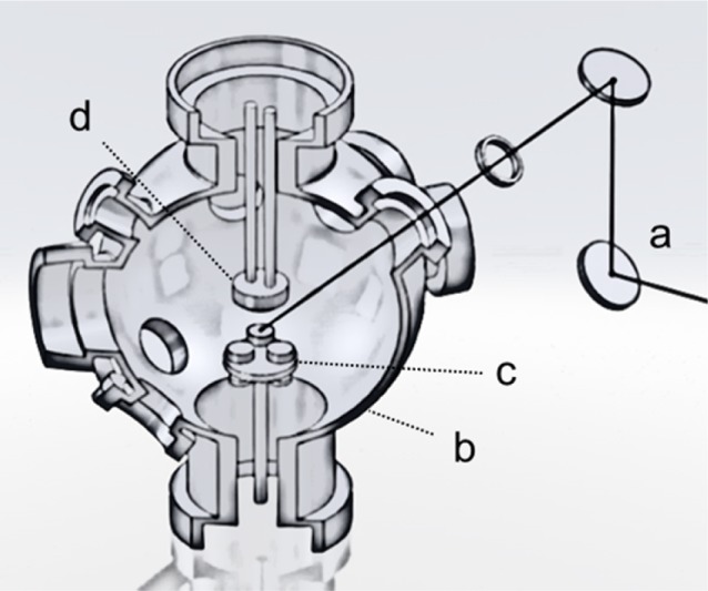
Pulsed laser deposition setup: (a) 248 nm KrF excimer laser, (b) vacuum chamber, (c) a target on the target carrousel, and (d) substrate holder.
2.1.3. Sputtering
Silver (Ag) metal back contacts were deposited by sputtering (BESTEC) from an Ag target (Kurt J. Lesker, 99.99% Pure), with a thickness of ∼100 nm. A custom-made shadow mask was used to define a grid of 13 × 13 round metal contacts, each with a diameter of 1.81 mm and corresponding contact area of 2.6 mm2. The deposition parameters were: preliminary base vacuum pressure, ∼1.5 × 10⁻⁷ Torr; Ar flow, 2.5 sccm; deposition pressure, ∼3.7 × 10⁻³ Torr; dc power, 100 W; coating time, 120 s; substrate rotation, 5 rpm; room temperature.
2.2. Library Preparation
Figure 4 shows the library preparation procedure: a 71.3 × 71.3 mm sized TCO-coated glass (fluorine-doped SnO2, TEC7 from Hartford) was cleaned and prepared for spray pyrolysis of TiO2 (see spray section above). In Figure 4b, the TiO2 layer was deposited in a horizontally spread thickness gradient spanning from 180 to 450 nm. Figure 4c shows the deposition of a Cu–O layer using pulsed laser deposition (PLD). The maximum thickness (∼900 nm) was formed at the center of the PLD deposition. The Cu–O was deposited from a CuO target under the previously mentioned conditions. The characteristically curved thickness profile was formed because of the expansion of the plasma plume in vacuum, distributing a material gradient to the library, which can be modeled by the gas-dynamic equations.71,74 Figure 4d shows the Ag back contacts that were sputtered through the aforementioned shadow mask. Finally, in Figure 4e, a common front contact of Sn/Pb alloy was soldered directly onto the TCO with an ultrasonic soldering iron.
Figure 4.
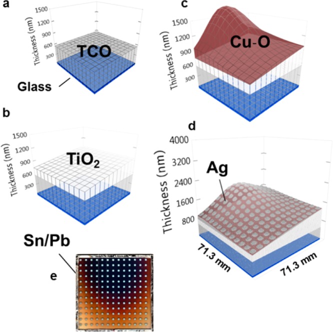
Fabrication of PV combinatorial device library (note that the thickness scale is adjusted to amplify the differences and represents real values as explained below): (a) TCO-coated glass (b) sprayed with a gradual compact TiO2 layer, followed by (c) pulsed laser deposition (PLD) of Cu–O with a characteristic shape originating from the laser plume. (d) Round Ag back contacts sputtered on top of the Cu–O layer with a 13 × 13 mask template, forming a grid of 169 distinct devices. Subsequently (e) a square common front contact is soldered ultrasonically from Sn/Pb directly onto the TCO.
2.3. Measurements and Calculations
2.3.1. Optical Measurements
Figure 5 presents the optical scanner. The scanner is capable of measuring total transmission (TT), total reflection (TR), and specular reflection (SR) with millimeter spatial resolution. The measurements allow the calculation of absorptance, diffuse reflection, light harvest efficiency (ηLH), the integrated internal quantum efficiency (in conjunction with the jV measurements), layer thickness, bandgap, and the nature of bandgap (i.e., direct/indirect), absorption coefficient, refractive indices, and carrier concentration.
Figure 5.
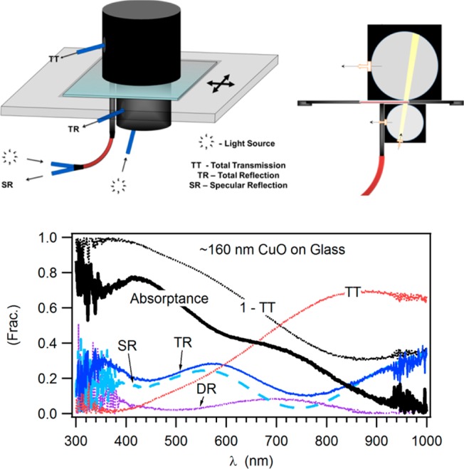
Optical scanner that measures: Total transmission (TT), total reflection (TR), and specular reflection (SR). Top left: Schematic 3D drawing. Top right: Cross-sectional view emphasizing the light distribution going to and from a sample. Bottom: Example of measured and calculated spectra for a single location in a library. Light is incident at a certain angle on a tested library via the inlet fiber of the TR integrating sphere. The transmitted light is collected in the upper integrating sphere, the TT sphere, whereas reflected light is collected in the lower integrating sphere. A SR probe complements the reflection measurements and allows the calculation of the diffuse reflection (DR). The calculated absorptance is = 1 – TT – TR.
Using optical fibers, light from a laser-excited xenon lamp (see LDLS in the solar simulator section) is directed to the SR probe and to the TR lower integrating sphere (QR400-7-VIS-NIR and ISP-30-6-R respectively, from ocean optics). The light from the TR sphere can be collected in the sphere itself or in the TT upper integrating sphere (ISP-80-8-R). The collected light from the probes is directed to a silicon photodiode array spectrophotometer tailored for spectral coverage in the UV-vis-NIR region with appropriate order sorting variable long-pass filters. The TT reference is taken with a bare glass of the same type and thickness as the substrate. TR reference is taken against a diffuse reflection standard comprised of Spectralon (WS-1-SL). Spectra from TR are corrected against the known WS-1-SL calibrated standard reference spectrum, and TT spectra are corrected against the spectrum of the glass part of the substrate, measured separately.
Dedicated software controls the measurement and records the data. First, it records the references, including dark noise of the detectors. Then, using the translational stage, it manipulates the library to the coordinates where back contacts will be deposited later to form the individual combinatorial solar cells. The software saves the data in three separate raw files, one for each measurement, and records details about the measurement in the database (sample name, integration time, number of averages, reference, spectrophotometer, etc.). Each raw file includes details about the scanning coordinates, a reference spectrum, dark reference spectrum, and the individual spectrum taken per coordinate.
2.3.2. Electrical Measurements under Solar Simulator
Current–voltage scans (jV-curves) are performed in the dark and under equivalent illumination of one sun AM1.5G. Automated analysis classifies jV-curves by their nature to photovoltaic or ohmic behavior, or raises cases where a measurement fails. Furthermore, automated analysis obtains the following parameters for each combinatorial cell: 1 sun short circuit photocurrent (Jsc), open circuit photovoltage (Voc), maximum power point (Mpp), fill factor (FF), current and voltage of maximum power point, shunt resistance (Rsh) and, series resistance (Rs).
Figure 6 shows a schematic representation of the solar simulator current–voltage high throughput scanner. A fiber coupled laser driven light source (LDLS), EQ-99FC from ENERGETIQ (a xenon lamp), is attenuated with an AM1.5G filter and neutral density filters, in order to match the spectral distribution and the overall intensity of AM1.5G emission in the region of 380–950 nm. The LDLS fiber outlet is fixed in a constant distance from the scanner stage. The Z arm, located at the center of the incident beam, pushes a spring suspended electric contact against the back contact (BC) of an individual cell. A second electrode is constantly connected to the common front contact (FC). The electrodes are wired to a computer controlled source meter (Keithley 2400 series).
Figure 6.
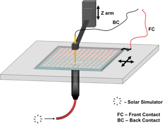
Schematic drawings of the solar simulator current–voltage high throughput scanner. The equivalent illumination of 1 sun, AM1.5G, is incident on the transparent front electrode. A current–voltage curve is measured for each combinatorial cell. The stage automatically scans each cell above the illumination spot via the Z arm. The scanner is capable of measuring libraries with the size of 71.3 × 71.3 mm. A typical cyclic scan of 169 cells takes 120 min for a potential window of 1.2 V, and a sweeping rate of 60 mV s–1, providing 240 points for each ascending-descending curve.
Dedicated homemade software controls the measurement and stores the data. Following prompt calibration, the software tells the stage to move to a set of cell coordinate, lowers the Z arm, and performs a jV scan. Voltage scanning is performed at a rate of 60 mV s–1.
2.3.3. Thickness
TiO2:
To obtain a thickness map of the TiO2 layer, optical measurements (TT and TR) were taken after the TiO2 spray and prior to the Cu–O deposition. The thickness, dTiO2(x, y), is calculated as
| 1 |
where αTiO2(λ) is the absorption coefficient of the sprayed TiO2 at λ = 475 nm. For TiO2, we calculated a value of αTiO2 (475 nm) = 2035 nm–1 using absorptance measurement and specific thickness measurements provided by focused ion beam and high resolution scanning electron microscopy (FIB and HRSEM respectively; see details in Figure S1 in Supporting Information). A(x, y, λ) is the absorptance at λ = 475 nm for each x,y position in the library, calculated with eq 3. Asub(λ) is the measured absorptance of the substrate alone, at the wavelength λ of calculation. Here we used TEC7 as the substrate material; at λ = 475 nm, it had a constant Asub (475 nm) of 9%. This value is common for all members of the library as the substrate is assumed homogeneous on the macroscopic level. This approximation was validated using electron microscopy and appears to provide good values. We note that this approximation works for sprayed TiO2 on TEC7, while some cells around the bottom right corner of the library diverged from the general linear trend of the TiO2 gradient.
Cu–O:
To obtain the Cu–O thickness profile, a second library was deposited directly on glass using the PLD, utilizing the exact deposition parameters as for the device library. Because the PLD sample holder masked the PLD plasma plume from deposition at the substrate edges, a well-defined step remained 1 mm from the edges of the glass substrate. On this remaining step, a sufficient number of measurements of thickness per position were made (see figure S2 in Supporting Information) with a profilometer to solve the following equation, derived from the gas-dynamic equations that describe the expansion of the plasma plume in vacuum:71,74
| 2 |
where dpld(x, y) is the measured or calculated thickness of the deposited material using PLD at a given x and y position (mm). d0 (nm) is the maximum thickness of the library. x0 and y0 (mm) are the position of the center of deposition with respect to the library coordinates. h, in mm, is the target-substrate distance as adjusted for deposition, which is known from the PLD geometry. nx and ny are fitted powers of the cosine.
The resulting deposition constants enable the calculation of the film thickness at any position in the library.
2.3.4. Raman
The low frequency vibrational modes of the oxide layers were characterized by Raman spectroscopy. Micro-Raman measurements were performed using a confocal Raman microscope with 532 nm laser excitation, a 100× objective, a 100 μm confocal pinhole, and an 1800 g/mm grating (LabRAM HR, Horiba Jobin Yvon Corporation). Raman mapping was implemented using autofocusing of the incident laser in order to ensure accurate comparison of scattering intensity across the device library. In particular, the library was exposed to the laser with the room darkened. The full power of the laser was 50 mW, and a neutral density filter of Optical Density 2 (OD2) was inserted in the beam path to prevent optical damage to the oxide layers. The acquisition time was 100 s per scanning interval (∼500 cm–1), with all measurements taken in air at room temperature.
2.3.5. Bandgap
To fit the bandgap of the absorber for all cells in the library as presented in Figure 9, two arrays of Tauc plots,81,82 for direct and indirect bandgap, indexed by cells coordinates, were calculated from absorptance and thickness measurements. A dedicated tool was used in order to group cells that complied with the following rules: a selected energy region (hν) between two cursors, and an r-squared value that is higher than a selected threshold (typically set to R2 > 0.99). The optional fits for each cell were reviewed and either αhν2 or αhν1/2 was selected, then the fit was approved. To ease the interpretation of the large amounts of data points, the resulting bandgaps were clustered into 5 groups in a bandgap histogram. The groups can be viewed in the examples shown in Figure 9b and in Table 2.
Figure 9.
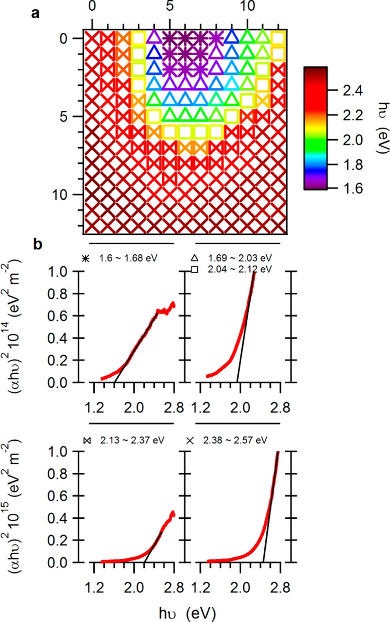
(a) Plot of fitted (direct) apparent bandgaps as a function of cell position, showing narrower bandgaps in the center of deposition, wider bandgaps in the periphery, and a gradual change in between. The bandgaps were calculated from absorptance spectra and the thickness of the absorber for each cell. The symbols of the cells are used to represent the partition of the library into five clusters of cells, having a bandgap in a specific range as shown in panel b. (b) Examples of bandgap fits taken from cells that represent clusters that have a common bandgap, showing also a variation in the absorption coefficient. The range of bandgaps and the representative symbol are shown on top of each example.
Table 2. Qualitative Relations between Cell Bandgap and the Copper-Oxide Composition.
| bandgap range (eV) | CuO | Cu4O3 | Cu2O | symbol |
|---|---|---|---|---|
| 1.6–1.68 | high | high | low | ∗ |
| 1.69–2.03 | low | high | high | Δ |
| 2.04–2.12 | high | high | □ | |
| 2.13–2.37 | low | high | ⋈ | |
| 2.38–2.57 | high | × |
2.3.6. Quantum Efficiency Calculations
Table 1. Symbols and Parameters Used in This Work.
| symbol | description | default value | units |
|---|---|---|---|
| Jsc | short circuit photocurrent | mA cm–2 | |
| Jcalcd | maximum theoretical calculated Jsc | mA cm–2 | |
| TT | total transmission | frac. | |
| TR | total reflection | frac. | |
| A | absorbance | frac. | |
| q | elementary charge of electron | 1.602 × 10⁻¹⁹ | C |
| φ | photon flux | m–2 s–1 |
For internal quantum efficiency calculations per library, spectra from TR and TT raw files are retrieved in parallel for each cell in the library. The absorptance for each cell in the library, A(x, y) is calculated as shown in eq 3:
| 3 |
where TT(x, y) and TR(x, y) are the total transmission and the total reflection (respectively) for each cell location with coordinates x and y. The integrated maximum theoretical short circuit photocurrent, Jcalcd, expected in each coordinate is calculated as shown in eq 4:
| 4 |
the absorbed fraction A(x, y, λ) in each wavelength (λ) is multiplied with φ(λ), the interpolated photon flux density for the same λ. The yield is integrated in the region of interest and multiplied by q, the elementary charge of an electron. The photon flux density spectrum, φ, was recorded after calibration of the solar simulator to reflect changes in light source intensity and in its spectral distribution.
To obtain the internal quantum efficiency per combinatorial cell, eq 5 is used:
| 5 |
where Jsc(x, y) is the 1 sun short-circuit photocurrent extracted from the measured jV curve for the same cell as the Jcalcd(x, y).
3. Results
Figure 7a shows a monochromatic absorptance profile of the stack TEC7|TiO2|Cu–O at a selected wavelength of 570 nm, where all copper oxide compounds absorb light. The profile is constructed from 13 × 13 absorptance spectra calculations made using eq 3. Four examples of calculated absorptance spectra are presented in Figure 7b, with tagged references to their position in the library. The spectra are different from each other because of the amount of deposited Cu–O, because of the resulting oxidation state of the Cu, and slightly because of the underlying TiO2 layer. The substrate contributes equal absorptance to all cells. The strong contribution of the absorber compared to the window layer is due to the higher extinction coefficient at the probed range, and to the larger differences in absorber layer thickness. The thickness gradient of the TiO2 is hardly evident here, as the absorptance difference between the thickest (right side) and thinnest (left) parts of the library is just several percent, while the difference in Cu–O absorptance reaches a delta of more than 80% at this wavelength.
Figure 7.
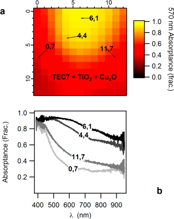
(a) Monochromatic absorptance fraction as a function of cell position, taken prior to back contact deposition. The chosen wavelength of 570 nm is common to all Cu–O compounds. The tagged locations refer to the selected absorptance spectra shown in panel b, highlighting the change in the spectral shape due to the variation in composition, and the change in absorptance fractions due to amount of material deposited.
From the 169 calculated absorptance spectra, the maximum expected photocurrents are calculated using eq 4. The map of maximum theoretical calculated photocurrent (Jcalcd) is presented in Figure 8a. The highest attainable photocurrent is expected in the cell indexed [6,1] with a value of ∼27 mA cm–2. A 100% absorption, at all wavelengths, at the calculated part of the spectrum would yield 34 mA cm–2 in our solar simulator. Thus in principle this absorber exhibits 79% light harvesting efficiency at this location. The lowest expected photocurrent, with a value of 8 mA cm–2, can be found at the bottom left corner of the library.
Figure 8.
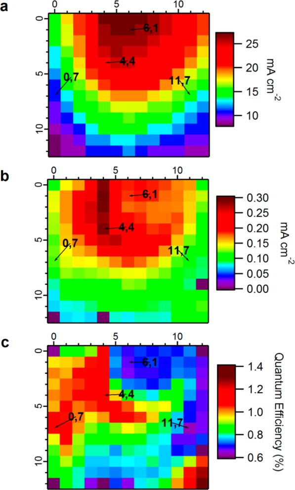
(a) Maximum theoretical short circuit photocurrent (Jcalcd) plotted as a function of cell position, for the solar simulator calibrated emission spectrum. (b) Plot of short circuit photocurrent (Jsc) as a function of cell position, extracted from jV scanning of the library under solar simulation (c) Plot of calculated internal quantum efficiency (IQE) as a function of cell position, showing that preferred PV activity occurs in locations that are not governed only by the amount of deposited absorber, in contrast to the trend shown in panels a and b.
Figure 8b is a map of the measured short circuit photocurrents (Jsc). Generally, the expected Jcalcd and measured Jsc maps have relative similarity. There are however mismatches that require highlighting. (1) the measured values are 2 orders of magnitude lower than the calculated ones, which is apparent from the color scale ranges of the two figures. (2) Cells calculated to generate the highest Jsc are not the ones that actually generate the highest measured Jsc. For example, point [4,4] generates 0.28 mA cm–2, which is 57% more photocurrent than point [6,1], while [6,1] was initially calculated to generate 12.5% more photocurrent than [4,4]. On the other hand, points calculated to generate unnoticeable photocurrent sometimes generate unexpected photocurrent (relatively). For example, point [0,7] with calculated 11 mA cm–2 and [11,7] with calculated 15 mA cm–2, in practice [0,7] generates 33% more photocurrent than [11,7].
Figure 8c is the internal quantum efficiency map. As previously explained, the measured Jsc values are simply divided by the calculated values. Generally, the IQE is in the range of 0.6 to 1.4%, reflecting the 2 orders of magnitude difference between measured and calculated photocurrents. The IQE map reveals that the library contains distinct regions of characteristics which clearly differ from the expected values.
Figure 9a shows the variation in the fitted bandgaps along the library. In the figure, the cells are divided into groups by their bandgap, where each is represented by a different symbol. Figure 9b shows examples of fitted bandgap plots taken from selected cells. The ranges of bandgap that these plots represent are mentioned in the figure and are the key for the symbols map in Figure 9a. Fitting for direct bandgap seemed to provide a better match than fitting for indirect bandgap, for all cells. The direct bandgap correlates with some of the literature values, together with the covariation of the bandgap with the amplitudes of the αhν2.42,83 It is important to note that there are several ambiguities regarding the bandgaps and the nature of the bandgap of copper oxide compounds for both experimental and calculated values found in the literature.
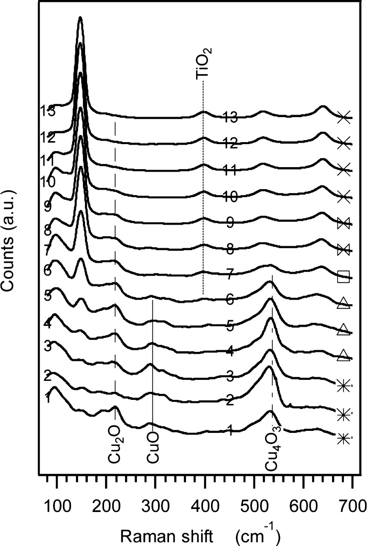
Figure 10 shows Raman spectra taken along the middle vertical, starting from a cell above the absorber’s center of deposition, down to the bottom of the library. Each spectrum in Figure 10 is marked by its vertical index, and is also correlated with the cell’s selected symbol according to Figure 9a. In Figure S3 in the Supporting Information all apparent Raman peak positions of CuO, Cu4O3, Cu2O,42,84,85 and crystalline anatase TiO286,87 were marked on an additional representation of the same data, shown there with no offset between the spectra, and on a logarithmic intensity scale. From both Raman figures, the verticals that are eventually shown in Figure 10 were selected since they provided a unique indication for each of the four dominant marked materials, residing in the library, in locations that show minimum convolution into other peaks. That is, the verticals in Figure 10 cross only spectra that show a signal for the material they represent. Thus from both Raman figures one can conclude the following: (a) The presence of Cu2O along the vertical cross-section is clear. Even when the Cu2O signal diminishes, as the absorber layer gets thinner, its presence is clearly observed in the logarithmic representation. (b) The Cu4O3 and CuO (unlike the Cu2O) are only found in the first 7 and first 6 cells, respectively, counting from the topmost cell along the line. (c) The strongest signal of the CuO is in the center of deposition, spectra taken at 10 and 15 mm from the top, and the Cu2O seems to relatively decrease when the CuO and Cu4O3 increase. (d) The TiO2 signal diminishes as the absorber layer becomes thicker than the penetration depth of the Raman laser beam.
Figure 10.
Raman spectra taken along a vertical line in the center of the library (column 7). The spectra are labeled by their vertical positions in the library (y), and with symbols (right side) that are taken from Figure 9a by their position, suggesting a correlation between composition and bandgap. The tags (CuO, Cu4O3, Cu2O, and TiO2) are unique Raman shifts for each of the materials. The lines cross only spectra that show a peak for a particular material, indicating the presence of Cu2O in all cells, CuO only in the center of deposition, Cu4O3 in a larger area around the center of deposition, and finally the disappearance of the underlying TiO2 underneath the thicker absorber layer. Refer to Figure S3 in the Supporting Information for a detailed representation of the Raman data.
The Raman results suggest that the absorber is a mixture of copper oxide compounds. Combined with the bandgap analysis, these results strengthen the observation that a qualitative compositional analysis, based on the Raman spectra, can be generalized to the groups in Figure 9. In other words, if the composition dictates the resulting observed bandgap, it can be assumed that the bandgap can represent the composition. This correlation is summarized in Table 2. Thus if we examine the groups again, we can conclude at this stage that cells resulting in a bandgap between 1.6 and 1.68 eV, with relatively low absorption coefficient values, are rich in the CuO phase, but still contain some Cu4O3 and Cu2O. On the other side of the library, cells with bandgap values between 2.38 and 2.57 eV, and with the highest absorption coefficient values, are composed almost entirely of a Cu2O phase. Between the two extremes there are three intermediate groups: one with no CuO and low presence of Cu4O3, with bandgaps ranging between 2.13 and 2.37 eV. Another, with no CuO and a higher presence of Cu4O3, and resulting bandgaps ranging between 2.04 and 2.12 eV. The last group, with a low presence of CuO, and a relatively high presence of the other two copper oxide compounds, have a resulting bandgap range between 1.69 and 2.03 eV.
The distinct regions that dominate the Jcalcd, Jsc, and IQE maps are dictated by the underlying thicknesses of the two active layers, the TiO2 and the Cu–O, and by the composition (and the resulting properties) of the last. It is highly informative to follow the thickness and composition contributions by plotting the maps as a function of these properties. Figure 11a–c shows three contour plots for the measured and calculated values presented in Figure 8, plotted as a function of the layers’ thicknesses. Due to multiple dimension representation issue, the composition is represented in a generalized way by the five groups’ symbols suggested above.
Figure 11.
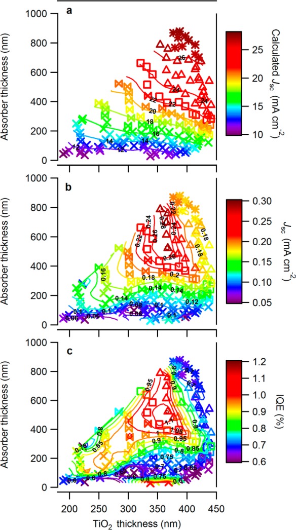
(a) Plot of maximum theoretical short circuit photocurrent (Jcalcd) as a function of TiO2 and Cu–O layer thicknesses. (b) Plot of short circuit photocurrent (Jsc) as a function of layer thicknesses. (c) Plot of calculated internal quantum efficiency (IQE) as a function of layer thicknesses. The symbols represent the bandgap/composition groups, showing that cells containing high levels of Cu4O3 (□ and Δ) have relatively enhanced IQE, whereas cells containing CuO have degraded IQE, and cells with Cu2O shows enhanced IQE only for specific cells.
Figure 11a clearly shows that Jcalcd increases mainly as a function of Cu–O thickness and slightly due to the light absorption of the TiO2, where the last argument is supported by the fact that the contour lines lean toward the right and are not parallel to the X-axis. The contour lines in Figure 11b, of the measured Jsc, show that the addition of Cu–O does tend to increase the photocurrent, but only to some extent. Figure 11c emphasizes the contrast between the two limits; some thin Cu–O cells show high IQE for cells with unnoticed measured Jsc and low Jcalcd, whereas cells calculated to show high Jcalcd had low Jsc and thus low IQE.
4. Discussion
The benefits of the IQE analysis are clearly depicted in Figure 8c and Figure 11c. A number of cells that show relatively low Jsc show relatively high IQE, correlated with the fact that less absorber was deposited in these regions. Overall, the IQE plots differ from the calculated and measured Jsc presented in Figure 8a and b or in Figure 11a and b, which makes these results a good example of the IQE method and how it can provide useful information about the materials and configurations used to fabricate the PV cells in the library. These findings call for a detailed examination of trends within the library which will follow below, but not before we discuss several other issues.
We note first, that due to the nature of the pulsed laser deposition of the Cu–O, under the reported experimental conditions, the library is better categorized by dividing it into clusters or sublibraries that hold similar properties, resulting from compositional mixtures of the 3 binary Cu–O compounds presented previously: CuO, Cu4O3, and Cu2O. To ease the interpretation, we assume that these sublibraries hold common properties such as morphology, level of crystallinity, crystal defect density, and the level of phase mixing. While these properties are not expected to be common for all the cells in the library, it is assumed that they are nearly constant within given regions around the center of deposition, given the expansion of the PLD plasma plume in vacuum. We address the sublibraries as suggested in the combined bandgap-composition analysis that was shown in Figure 9, Figure 10, and summarized in Table 2.
We also wish to emphasize the physical implications of the IQE data. It is the kinetic competitions and thermodynamic driving forces that define the performance of photovoltaic cells. Amid many favorable and unfavorable processes that occur in the cell, the first is the absorption of photons in the active layer. It is quantified as light harvesting efficiency (ηLH), which is the initial theoretical amount of electrons available for the system. The monochromatic short circuit photocurrent, Jsc, can generally be described by the following equation:
| 6 |
where ηCS and ηCol are charge separation and collection efficiencies respectively. Combining eq 6 with eqs 4 and 5 yields: IQE = ηCSηCol. This is a very simplified solution that possesses valuable information about the combinatorial PV devices. Although it does not explain whether losses are due to poor charge separation or collection, as seen below, it does substantially streamline the investigation.
The largest sublibrary, residing at the periphery of the absorber deposition, consists mainly of Cu2O. The bandgaps in this group are the highest, implying the lowest light harvesting efficiency in terms of spectral coverage. Considering that these cells also have the thinnest absorber layer, they are the weakest light harvesting cells in the library. This is expressed by the fact that these cells are at the bottom of the Jcalcd scale in the theoretical photocurrent plots. Furthermore, the weak measured Jsc for these cells makes them un-noticed when plotted together with cells having improved light harvesting efficiency, namely the cells from other sublibraries. On the contrary, the IQE shows that this group of cells performs relatively more efficiently and suggests two trends: 1. that devices with much thicker or, surprisingly, much thinner Cu2O layers relative to the TiO2 layer, actually perform better, and 2. intermediate thickness ratios show the worst performances. To elucidate this argument, the results from Figure 11 are plotted again in Figure S4 in the Supporting Information, this time with logarithmic scale for the absorber thickness, and furthermore the fitted bandgaps from Figure 9a are plotted in the same fashion, i.e. as a function of logarithmic thickness of Cu–O versus linear thickness of TiO2. The logarithmic presentation stretches the scale of the thin part of the Cu–O and parses the cells in this densely populated region. This presentation and the comparison with the adjacent bandgaps plot raise the following suspicion: as mentioned above, since the thickness and bandgap are covarying in this library (bandgap as an expression of composition), it is possible that a several milli-eV drop in the bandgap indicates a composition with an improved IQE. In other words, the thickest cells in this sublibrary could have been related to the next sublibrary, where more cells showed improved IQE, while the remaining cells in this peripheral sublibrary are actually composed of an inefficient absorber, that the less deposition of it, the more pronounced the efficiency of the underlying TiO2.88
The smallest sublibrary, found at the center of the PLD deposition, contains the narrowest bandgaps and the thickest absorbing layers. This potentially should have been the best performing sublibrary, but it is not. This sublibrary consists of all three copper oxide compounds mentioned in the introduction, with the highest presence of CuO. The lowest IQE values in this sublibrary can suggest that the CuO presence harms the PV activity of the other two compounds. However other options should be eliminated first, as discussed further below.
The remaining three sublibraries bridge between the two previously sublibraries. Intriguing observations are: first, that the highest Jsc values are found in one group (triangles), while the highest IQE values are found in another (squares) and both contain high levels of paramelaconite (Cu4O3). The second observation, for all the groups, is the lower ratios of Cu–O:TiO2 within each of these two groups tends to show degraded IQE. To emphasis the last argument, we propose a data representation as in Figure 12.
Figure 12.
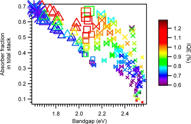
IQE plotted vs bandgap and absorber fraction in the total stack. The sizes of the symbols correlate with the absorber thickness. The figure suggests that the bandgap, the composition and the ratio between the layers play significant roles for the IQE and suggest a correlation between these parameters that may be more significant from the absolute layers thickness representation above.
Figure 12 proposes an alternative representation for the aforementioned discussion. This, however, is limited by a multiple dimension representation issue. The plot shows the changes in IQE as a function of bandgap and of Cu–O:TiO2 ratio (normalized to the overall thickness) and the limit is that it discards the absolute thickness data (even though the Cu–O is represented by the size of the symbols, it is not an ideal quantifiable representation). This representation in some ways is the answer to the schematic energy band diagram shown in Figure 1 in the introduction. The benefit of plotting such figures for several thicknesses is that it may provide information on the source of limit that governs heterojunction solar cell performance. That is, to find whether it is the charge collection, or charge separation that limits the overall IQE to the range of 1%. It is important to emphasize the limitation of this plot in that it can be drawn for many different devices that maintain similar thickness ratios, but have different IQE. Nonetheless, the data, once correlated with Figure 11c, is sufficient to draw the general trend that at a given bandgap (and thus composition), when the Cu–O:TiO2 ratio increases, the IQE increases (becomes red) until a certain ratio is reached, and then it starts to decline. This is apparent down to ∼2.05 eV where below this value there are not enough cells to draw this trend conclusively. Similarly, there are not enough cells to conclude about the aforementioned opposite trend, where for very thin absorber the IQE starts to increase.
In the light of these observations, a sequential design of experiment should consider that future libraries be fabricated with a thinner TiO2 layer or with a different material. Given the fact that the CuO containing cells are at the maximum edge of their light harvesting capabilities, further increasing the Cu–O:TiO2 ratio by thickening the CuO layer seems like an erroneous approach. Furthermore, moving toward pure CuO seems erroneous as well, as this tends to show a decline in the absorption coefficient that will require an even thicker layer of CuO to reach the same light harvesting efficiency while its IQE is already low. Pure or mixed Cu4O3 based libraries are definitely an expected direction as the presence of these materials showed the highest PV activity. As the results are gathered in a database, it is very likely that common measured properties, such as bandgap and composition, can unify libraries or sublibraries (as shown above) into larger data sets that span beyond a single library.
5. Conclusions
Using the combinatorial IQE, bandgap, composition, and thickness techniques we gather several empirical observations that are unique to the binary Cu–O compounds, and are important for the correlation of these materials’ intrinsic properties and their photovoltaic activity, once placed in conjunction with an n-type wide bandgap semiconductor. We observe a continuous variation in bandgap and composition along the pulsed laser deposition profile, changing from 1.6 eV in the center of deposition, toward 2.57 eV at the periphery. The change in bandgap is supported by a change in the composition blend; the narrowest bandgaps are maintained by a higher presence of CuO, whereas the widest bandgaps are almost entirely due to pure Cu2O. The presence of Cu4O3 shifts the bandgaps to a region between 1.6 and 2.12 eV, depending on the other Cu–O compounds present, and shows the preferred photovoltaic activity. These last two facts may contradict some publications claiming to have either CuO or Cu2O in the higher performing heterojunction PV’s with reported bandgaps around 2.1 eV. The purity of CuO in our library was insufficient to observe an indirect bandgap although it did tend to reduce the absorption coefficient of the cells. The presence of the CuO, though, seemed detrimental for the photovoltaic activity of the other two Cu–O compounds, however, this calls for a deeper investigation of the correlation we observed between the bandgap, the layers’-ratio, and the absolute thickness, which suggests that the narrower the bandgap, the higher the Cu–O:TiO2 ratio should be in order to maintain proper charge separation and collection efficiencies. As for the least studied Cu4O3, we find that its presence is favored in terms of PV activity, and should be thoroughly investigated as a single material layer, host or dopant.
The internal quantum efficiency analysis is relatively straightforward, and relies on the basic characterization of solar cells, jV curves under solar simulation, and UV–vis–NIR spectroscopy. The analysis quantifies the light harvesting efficiency as well as the amount of light lost to diffuse/specular reflection and to transmission. From IQE calculations, combined losses due to charge separation and collection can be addressed. As concluded above, the incorporation of this analysis in combinatorial PV research provides a substantial addition to the investigation cycle for device physics and material studies via data representation and data mining.
Acknowledgments
The authors thank Dr. Robert Lovrincic, Dr. Hanoch Senderowitz, and Mr. Avi Yosipof for fruitful discussions, Mr. Udi Nemschitz for support in building the various scanning systems, Mr. Roy Gur Ari for the 3D PLD diagram, and Mr. Shachaf Poran for his assistance in programing the bandgap tool.
Supporting Information Available
Table of PLD deposition parameters, cross-sectional micrographs of TiO2 on TEC7, taken using electron microscopy and sectioned using focused ion beam milling for TiO2 thickness analysis, profilometer results of PLD deposition profile, Raman spectra of a vertical line in the center of the library shown on logarithmic scale with no offsets and with all peaks labeled for CuO, Cu4O3, Cu2O, and TiO2), plots of Jcalcd, Jsc, BG, and IQE as a function of logarithmic absorber and linear TiO2 thicknesses, and plots of cell performance as a function bandgap and the absorber fraction in the total stack. This material is available free of charge via the Internet at http://pubs.acs.org.
This study was funded by the European Commission under the FP7 AllOxidePV project “Novel Composite Oxides by Combinatorial Material Synthesis for Next Generation All-Oxide-Photovoltaics”, number 309018. S.R. acknowledges financial support from the European Union within the FP7 framework (Marie Curie Intra-European Fellowship for Career Development).
The authors declare no competing financial interest.
Supplementary Material
References
- Jäger-Waldau A. Thin Film Photovoltaics: Markets and Industry. Int. J. Photoenergy 2012, 2012, 1–6. [Google Scholar]
- Wadia C.; Alivisatos a. P.; Kammen D. M. Materials Availability Expands the Opportunity for Large-Scale Photovoltaics Deployment. Environ. Sci. Technol. 2009, 43, 2072–7. [DOI] [PubMed] [Google Scholar]
- Nayak P. K.; Bisquert J.; Cahen D. Assessing Possibilities and Limits for Solar Cells. Adv. Mater. 2011, 23252870–2876. [Google Scholar]
- Lewis N. S. Toward Cost-Effective Solar Energy Use. Science 2007, 3155813798–801. [DOI] [PubMed] [Google Scholar]
- Razykov T. M.; Ferekides C. S.; Morel D.; Stefanakos E.; Ullal H. S.; Upadhyaya H. M. Solar Photovoltaic Electricity: Current Status and Future Prospects. Sol. Energy 2011, 8581580–1608. [Google Scholar]
- O’Regan B.; Gratzel M. A Low-Cost, High-Efficiency Solar Cell Based on Dye-Sensitized Colloidal TiO2 Films. Nature 1991, 3536346737–740. [Google Scholar]
- Peter L. M. The Grätzel Cell: Where Next?. J. Phys. Chem. Lett. 2011, 2151861–1867. [Google Scholar]
- Hagfeldt A.; Boschloo G.; Sun L.; Kloo L.; Pettersson H. Dye-Sensitized Solar Cells. Chem. Rev. 2010, 110106595–6663. [DOI] [PubMed] [Google Scholar]
- Rühle S.; Shalom M.; Zaban A. Quantum-Dot-Sensitized Solar Cells. ChemPhysChem 2010, 11, 2290–304. [DOI] [PubMed] [Google Scholar]
- Jørgensen M.; Norrman K.; Gevorgyan S. a.; Tromholt T.; Andreasen B.; Krebs F. C. Stability of polymer solar cells. Adv. Mater. 2012, 24, 580–612. [DOI] [PubMed] [Google Scholar]
- Snaith H. J. Estimating the Maximum Attainable Efficiency in Dye-Sensitized Solar Cells. Adv. Funct. Mater. 2010, 20, 13–19. [Google Scholar]
- Mittiga A.; Salza E.; Sarto F.; Tucci M.; Vasanthi R. Heterojunction Solar Cell with 2% Efficiency Based on a Cu2O Substrate. Appl. Phys. Lett. 2006, 88, 163502. [Google Scholar]
- Bisquert J.; Cahen D.; Hodes G.; Rühle S.; Zaban A. Physical Chemical Principles of Photovoltaic Conversion with Nanoparticulate, Mesoporous Dye-Sensitized Solar Cells. J. Phys. Chem. B 2004, 108248106–8118. [Google Scholar]
- Rühle S.; Anderson A. Y.; Barad H.-N.; Kupfer B.; Bouhadana Y.; Rosh-Hodesh E.; Zaban A. All-Oxide Photovoltaics. J. Phys. Chem. Lett. 2012, 3, 3755–3764. [DOI] [PubMed] [Google Scholar]
- Olsen L. C.; Addis F. W.; Miller W. Experimental and Theoretical Studies of Cu2O Solar Cells. Sol. Cells 1982, 73247–279. [Google Scholar]
- Olsen L. C.; Bohara R. C.; Urie M. W. Explanation for Low-Efficiency Cu2O Schottky-Barrier Solar Cells. Appl. Phys. Lett. 1979, 34147. [Google Scholar]
- Iwanowski R. J.; Trivich D. Enhancement of the Photovoltaic Conversion Efficiency in Cu/Cu2O Schottky Barrier Solar Cells by H+ Ion Irradiation. Phys. Stat. Sol. (a) 1986, 95, 735–741. [Google Scholar]
- Han K.; Tao M. Electrochemically Deposited p–n Homojunction Cuprous Oxide Solar Cells. Sol. Energy Mater. Sol. Cells 2009, 93, 153–157. [Google Scholar]
- McShane C. M.; Choi K.-S. Junction Studies on Electrochemically Fabricated p–n Cu2O Homojunction Solar Cells for Efficiency Enhancement. Phys. Chem. Chem. Phys. 2012, 14, 6112–8. [DOI] [PubMed] [Google Scholar]
- McShane C. M.; Siripala W. P.; Choi K.-S. Effect of Junction Morphology on the Performance of Polycrystalline Cu2O Homojunction Solar Cells. J. Phys. Chem. Lett. 2010, 1, 2666–2670. [Google Scholar]
- Wei H. M.; Gong H. B.; Chen L.; Zi M.; Cao B. Q. Photovoltaic Efficiency Enhancement of Cu2O Solar Cells Achieved by Controlling Homojunction Orientation and Surface Microstructure. J. Phys. Chem. C 2012, 116, 10510–10515. [Google Scholar]
- Herion J.; Niekisch E. A.; Scharl G. Investigation of Metal Oxide/Cuprous Oxide Heterojunction Solar Cells. Sol. Energy Mater. 1980, 41101–112. [Google Scholar]
- Jeong S. S.; Mittiga A.; Salza E.; Masci A.; Passerini S. Electrodeposited ZnO/Cu2O Heterojunction Solar Cells. Electrochim. Acta 2008, 5352226–2231. [Google Scholar]
- Katayama J.; Ito K.; Matsuoka M.; Tamaki J. Performance of Cu2O/ZnO Solar Cell Prepared by Two-Step Electrodeposition. J. Appl. Electrochem. 2004, 347687–692. [Google Scholar]
- Minami T.; Nishi Y.; Miyata T.; Nomoto J.-i. High-Efficiency Oxide Solar Cells with ZnO/Cu2O Heterojunction Fabricated on Thermally Oxidized Cu2O Sheets. Appl. Phys. Express 2011, 4, 062301. [Google Scholar]
- Nishi Y.; Miyata T.; Minami T. Effect of Inserting a Thin Buffer Layer on the Efficiency in n-ZnO/p-Cu2O Heterojunction Solar Cells. J. Vac. Sci. Technol., A 2012, 30, 04D103. [Google Scholar]
- Wijesundera R. P. Fabrication of the CuO/Cu2O Heterojunction Using an Electrodeposition Technique for Solar Cell Applications. Semicond. Sci. Technol. 2010, 25, 045015. [Google Scholar]
- Cui J.; Gibson U. J. A Simple Two-Step Electrodeposition of Cu2O/ZnO Nanopillar Solar Cells. J. Phys. Chem. C 2010, 114, 6408–6412. [Google Scholar]
- Musselman K. P.; Wisnet A.; Iza D. C.; Hesse H. C.; Scheu C.; MacManus-Driscoll J. L.; Schmidt-Mende L. Strong Efficiency Improvements in Ultra-Low-Cost Inorganic Nanowire Solar Cells. Adv. Mater. 2010, 22, E254-8. [DOI] [PubMed] [Google Scholar]
- Musselman K. P.; Marin A.; Wisnet A.; Scheu C.; MacManus-Driscoll J. L.; Schmidt-Mende L. A Novel Buffering Technique for Aqueous Processing of Zinc Oxide Nanostructures and Interfaces, and Corresponding Improvement of Electrodeposited ZnO-Cu2O Photovoltaics. Adv. Funct. Mater. 2011, 21, 573–582. [Google Scholar]
- Musselman K. P.; Marin A.; Schmidt-Mende L.; MacManus-Driscoll J. L. Incompatible Length Scales in Nanostructured Cu2O Solar Cells. Adv. Funct. Mater. 2012, 22, 2202–2208. [Google Scholar]
- Yuhas B. D.; Yang P. Nanowire-Based All-Oxide Solar Cells. J. Am. Chem. Soc. 2009, 131, 3756–61. [DOI] [PubMed] [Google Scholar]
- de Jongh P. E.; Vanmaekelbergh D.; Kelly J. J. Cu2O: Electrodeposition and Characterization. Chem. Mater. 1999, 11, 3512–3517. [Google Scholar]
- Li D.; Chien C.-J.; Deora S.; Chang P.-C.; Moulin E.; Lu J. G. Prototype of a Scalable Core–Shell Cu2O/TiO2 Solar Cell. Chem. Phys. Lett. 2011, 501, 446–450. [Google Scholar]
- Minami T.; Nishi Y.; Miyata T. High-Efficiency Cu2O-Based Heterojunction Solar Cells Fabricated Using a Ga2O3 Thin Film as N-Type Layer. Appl. Phys. Express 2013, 6, 044101. [Google Scholar]
- Shockley W.; Queisser H. J. Detailed Balance Limit of Efficiency of p–n Junction Solar Cells. J. Appl. Phys. 1961, 323510–519. [Google Scholar]
- Koffyberg F. P. A Photoelectrochemical Determination of the Position of the Conduction and Valence Band Edges of p-Type CuO. J. Appl. Phys. 1982, 53, 1173. [Google Scholar]
- Marabelli F.; Parravicini G.; Salghetti-Drioli F. Optical Gap of CuO. Phys. Rev. B 1995, 52, 1433–1436. [DOI] [PubMed] [Google Scholar]
- Tanaka T. Optical Constants of Polycrystalline 3d Transition Metal Oxides in the Wavelength Region 350 to 1200 nm. Jpn. J. Appl. Phys. 1979, 18, 1043–1047. [Google Scholar]
- Ito T.; Yamaguchi H.; Masumi T.; Adachi S. Optical Properties of CuO Studied by Spectroscopic Ellipsometry. J. Phys. Soc. Jpn. 1998, 67, 3304–3309. [Google Scholar]
- Ghijsen J.; Tjeng L.; van Elp J.; Eskes H.; Westerink J.; Sawatzky G.; Czyzyk M. Electronic Structure of Cu2O and CuO. Phys. Rev. B 1988, 381611322–11330. [DOI] [PubMed] [Google Scholar]
- Meyer B. K.; Polity A.; Reppin D.; Becker M.; Hering P.; Klar P. J.; Sander T.; Reindl C.; Benz J.; Eickhoff M.; Heiliger C.; Heinemann M.; Bläsing J.; Krost A.; Shokovets S.; Müller C.; Ronning C. Binary Copper Oxide Semiconductors: From Materials Towards Devices. Phys. Stat. Sol. (b) 2012, 24981487–1509. [Google Scholar]
- Mao S. S. High Throughput Combinatorial Screening of Semiconductor Materials. Appl. Phys. A: Mater. Sci. Process. 2011, 105, 283–288. [Google Scholar]
- Danielson E.; Golden J. H.; McFarland E. W.; Reaves C. M.; Weinberg H. W.; Di Wu X. A Combinatorial Approach to the Discovery and Optimization of Luminescent Materials. Nature 1997, 389, 944–948. [Google Scholar]
- Cui J.; Chu Y. S.; Famodu O. O.; Furuya Y.; Hattrick-Simpers J.; James R. D.; Ludwig A.; Thienhaus S.; Wuttig M.; Zhang Z.; Takeuchi I. Combinatorial Search of Thermoelastic Shape-Memory Alloys with Extremely Small Hysteresis Width. Nat. Mater. 2006, 5, 286–90. [DOI] [PubMed] [Google Scholar]
- Stepanovich A.; Sliozberg K.; Schuhmann W.; Ludwig A. Combinatorial Development of Nanoporous WO3 Thin Film Photoelectrodes for Solar Water Splitting by Dealloying of Binary Alloys. Int. J. Hydrogen Energy 2012, 37, 11618–11624. [Google Scholar]
- Jaramillo T. F.; Baeck S.-H.; Kleiman-Shwarsctein A.; Choi K.-S.; Stucky G. D.; McFarland E. W. Automated Electrochemical Synthesis and Photoelectrochemical Characterization of Zn1–xCo(x)O Thin Films for Solar Hydrogen Production. J. Comb. Chem. 2005, 7, 264–71. [DOI] [PubMed] [Google Scholar]
- Romero J. V.; Smith J. W. H.; Sullivan B. M.; Croll L. M.; Dahn J. R. SO2 and NH3 Gas Adsorption on a Ternary ZnO/CuO/CuCl2 Impregnated Activated Carbon Evaluated Using Combinatorial Methods. ACS Comb. Sci 2012, 14131–37. [DOI] [PubMed] [Google Scholar]
- Kafizas A.; Parkin I. P. Inorganic Thin-Film Combinatorial Studies for Rapidly Optimizing Functional Properties. Chem. Soc. Rev. 2012, 41, 738–81. [DOI] [PubMed] [Google Scholar]
- Potyrailo R.; Rajan K.; Stoewe K.; Takeuchi I.; Chisholm B.; Lam H. Combinatorial and High-Throughput Screening of Materials Libraries: Review of State of the Art. ACS Comb. Sci 2011, 13, 579–633. [DOI] [PubMed] [Google Scholar]
- Potyrailo R. A.; Mirsky V. M. Combinatorial and High-Throughput Development of Sensing Materials: The First 10 Years. Chem. Rev. 2008, 108, 770–813. [DOI] [PubMed] [Google Scholar]
- Takeuchi I.; Lauterbach J.; Fasolka M. J. Combinatorial Materials Synthesis. Mater. Today 2005, 8, 18–26. [Google Scholar]
- Barber Z. H.; Blamire M. G. High Throughput Thin Film Materials Science. Mater. Sci. Technol. 2008, 247757–770. [Google Scholar]
- Finn M. G. Combinatorial Science. J. Phys. Chem. Lett. 2012, 3, 3811–3811. [DOI] [PubMed] [Google Scholar]
- Kolb H. C.; Finn M. G.; Sharpless K. B. Click Chemistry: Diverse Chemical Function from a Few Good Reactions. Angew. Chem., Int. Ed. 2001, 40, 2004–2021. [DOI] [PubMed] [Google Scholar]
- Choi W. C.; Kim J. D.; Woo S. I. Quaternary Pt-Based Electrocatalyst for Methanol Oxidation by Combinatorial Electrochemistry. Catal. Today 2002, 74, 235–240. [Google Scholar]
- Teichler A.; Eckardt R.; Hoeppener S.; Friebe C.; Perelaer J.; Senes A.; Morana M.; Brabec C. J.; Schubert U. S. Combinatorial Screening of Polymer:Fullerene Blends for Organic Solar Cells by Inkjet Printing. Adv. Energy Mater. 2011, 1, 105–114. [Google Scholar]
- Hänsel H.; Zettl H.; Krausch G.; Schmitz C.; Kisselev R.; Thelakkat M.; Schmidt H.-W. Combinatorial Study of the Long-Term Stability of Organic Thin-Film Solar Cells. Appl. Phys. Lett. 2002, 81112106. [Google Scholar]
- Godovsky D.; Chen L.; Pettersson L. The use of combinatorial materials development for polymer solar cells. Adv. Mater. 2000, 54, 47–54. [Google Scholar]
- Lin E.-C.; Cole J. J.; Jacobs H. O. Gas phase electrodeposition: a programmable multimaterial deposition method for combinatorial nanostructured device discovery. Nano Lett. 2010, 10, 4494–500. [DOI] [PubMed] [Google Scholar]
- Haber J.; Gerein N.; Hatchard T.; Versavel M., Combinatorial discovery of new thin film photovoltaics. Photovoltaic Specialists Conference, 2005. Conference Record of the Thirty-first IEEE2005, 155-158.
- Wang Q. Combinatorial Hot-Wire CVD Approach to Exploring Thin-Film Si Materials and Devices. Thin Solid Films 2003, 430, 78–82. [Google Scholar]
- Wang Q.; Liu F.; Han D. High-Throughput Chemical Vapor Deposition System and Thin-Film Silicon Library. Macromol. Rapid Commun. 2004, 25, 326–329. [Google Scholar]
- Wang Q.; Moutinho H.; To B.; Perkins J.; Ginley D.; Branz H. M.; Tessler L. R.; Han D. Combinatorial Approach to Thin-Film Silicon Materials and Devices. Mater. Res. Soc. Symp. Proc. 2003, 762, A9.1. [Google Scholar]
- Jang J. S.; Lee J.; Ye H.; Fan F. R. F.; Bard A. J. Rapid Screening of Effective Dopants for Fe2O3 Photocatalysts with Scanning Electrochemical Microscopy and Investigation of Their Photoelectrochemical Properties. J. Phys. Chem. C 2009, 113, 6719–6724. [Google Scholar]
- Perkins J.; Paudel T.; Zakutayev a.; Ndione P.; Parilla P.; Young D.; Lany S.; Ginley D.; Zunger a.; Perry N.; Tang Y.; Grayson M.; Mason T.; Bettinger J.; Shi Y.; Toney M. Inverse Design Approach to Hole Doping in Ternary Oxides: Enhancing p-Type Conductivity in Cobalt Oxide Spinels. Phys. Rev. B 2011, 84, 1–8. [Google Scholar]
- Zakutayev A.; Paudel T.; Ndione P.; Perkins J.; Lany S.; Zunger A.; Ginley D. Cation off-Stoichiometry Leads to High p-Type Conductivity and Enhanced Transparency in Co2ZnO4 and Co2NiO4 Thin Films. Phys. Rev. B 2012, 85, 085204. [Google Scholar]
- Thelakkat M.; Schmitz C.; Neuber C.; Schmidt H.-W. Materials Screening and Combinatorial Development of Thin Film Multilayer Electro-Optical Devices. Macromol. Rapid Commun. 2004, 251204–223. [Google Scholar]
- Neuber C.; Bate M.; Thelakkat M.; Schmidt H.-W.; Hansel H.; Zettl H.; Krausch G. Combinatorial Preparation and Characterization of Thin-Film Multilayer Electro-Optical Devices. Rev. Sci. Instrum. 2007, 787072216–11. [DOI] [PubMed] [Google Scholar]
- Treharne R. E.; Hutchings K.; Lamb D. A.; Irvine S. J. C.; Lane D.; Durose K. Combinatorial Optimization of Al-Doped ZnO Films for Thin-Film Photovoltaics. J. Phys. D: Appl. Phys. 2012, 45, 335102. [Google Scholar]
- Anisimov S. I.; Bäuerle D.; Luk’yanchuk B. S. Gas Dynamics and Film Profiles in Pulsed-Laser Deposition of Materials. Phys. Rev. B 1993, 481612076–12081. [DOI] [PubMed] [Google Scholar]
- Christen H. M.; Rouleau C. M.; Ohkubo I.; Zhai H. Y.; Lee H. N.; Sathyamurthy S.; Lowndes D. H. An Improved Continuous Compositional-Spread Technique Based on Pulsed-Laser Deposition and Applicable to Large Substrate Areas. Rev. Sci. Instrum. 2003, 7494058. [Google Scholar]
- Ohkubo I.; Christen H. M.; Khalifah P.; Sathyamurthy S.; Zhai H. Y.; Rouleau C. M.; Mandrus D. G.; Lowndes D. H. Continuous Composition-Spread Thin Films of Transition Metal Oxides by Pulsed-Laser Deposition. Appl. Surf. Sci. 2004, 2231–335–38. [Google Scholar]
- Tyunina M.; Leppävuori S. Effects of Laser Fluence, Size, and Shape of the Laser Focal Spot in Pulsed Laser Deposition Using a Multielemental Target. J. Appl. Phys. 2000, 87, 8132. [Google Scholar]
- Barnes P. R. F.; Anderson A. Y.; Koops S. E.; Durrant J. R.; O’Regan B. C. Electron Injection Efficiency and Diffusion Length in Dye-Sensitized Solar Cells Derived from Incident Photon Conversion Efficiency Measurements. J. Phys. Chem. C 2008, 11331126–1136. [Google Scholar]
- Barnes P. R. F.; Anderson A. Y.; Koops S. E.; Durrant J. R.; O’Regan B. C. Electron Injection Efficiency and Diffusion Length in Dye-Sensitised Solar Cells Derived from Incident Photon Conversion Efficiency Measurements. J. Phys. Chem. C 2009, 1132812615–12615. [Google Scholar]
- Halme J.; Boschloo G.; Hagfeldt A.; Lund P. Spectral Characteristics of Light Harvesting, Electron Injection, and Steady-State Charge Collection in Pressed TiO2 Dye Solar Cells. J. Phys. Chem. C 2008, 112145623–5637. [Google Scholar]
- Soedergren S.; Hagfeldt A.; Olsson J.; Lindquist S.-E. Theoretical Models for the Action Spectrum and the Current-Voltage Characteristics of Microporous Semiconductor Films in Photoelectrochemical Cells. J. Phys. Chem. 1994, 98215552–5556. [Google Scholar]
- O’Regan B.; Schwartz D. T. Efficient Dye-Sensitized Charge Separation in a Wide-Band-Gap p–n Heterojunction. J. Appl. Phys. 1996, 8084749–4754. [Google Scholar]
- Rühle S.; Yahav S.; Greenwald S.; Zaban A. Importance of Recombination at the TCO/Electrolyte Interface for High Efficiency Quantum Dot Sensitized Solar Cells. J. Phys. Chem. C 2012, 1163317473–17478. [Google Scholar]
- Tauc J. Optical Properties and Electronic Structure of Amorphous Ge and Si. Mater. Res. Bull. 1968, 3, 37–46. [Google Scholar]
- Tauc J.; Grigorovici R.; Vancu A. Optical Properties and Electronic Structure of Amorphous Germanium. phys. stat. sol. (b) 1966, 15, 627–637. [Google Scholar]
- Pierson J. F.; Thobor-Keck A.; Billard A. Cuprite, Paramelaconite and Tenorite Films Deposited by Reactive Magnetron Sputtering. Appl. Surf. Sci. 2003, 2103–4359–367. [Google Scholar]
- Chrzanowski J.; Irwin J. C. Raman Scattering from Cupric Oxide. Solid State Commun. 1989, 70, 11–14. [Google Scholar]
- Debbichi L.; Marco de Lucas M. C.; Pierson J. F.; Krüger P. Vibrational Properties of CuO and Cu4O3 from First-Principles Calculations, and Raman and Infrared Spectroscopy. J. Phys. Chem. C 2012, 1161810232–10237. [Google Scholar]
- Ohsaka T.; Izumi F.; Fujiki Y. Raman Spectrum of Anatase, TiO2. J. Raman Spectrosc. 1978, 7, 321–324. [Google Scholar]
- Rangel-Porras G.; Ramos-Ramírez E.; Torres-Guerra L. M. Mesoporous Characteristics of Crystalline Indium-Titania Synthesized by the Sol–Gel Route. J. Porous Mater. 2009, 17, 69–78. [Google Scholar]
- Kamat P. V. TiO2 Nanostructures: Recent Physical Chemistry Advances. J. Phys. Chem. C 2012, 1162211849–11851. [Google Scholar]
Associated Data
This section collects any data citations, data availability statements, or supplementary materials included in this article.


