Abstract
We describe a design methodology for on-chip magnetic bead label detectors based on Hall-effect sensors. Signal errors caused by the label-binding process and other factors that limit the minimum detection area are quantified and adjusted to meet typical assay accuracy standards. The methodology is demonstrated by designing an 8192 element Hall sensor array, implemented in a commercial 0.18 μm CMOS process with single-mask postprocessing. The array can quantify a 1% surface coverage of 2.8 μm beads in 30 seconds with a coefficient of variation of 7.4%. This combination of accuracy and speed makes this technology a suitable detection platform for biological assays based on magnetic bead labels.
Index Terms: Assay, biosensor, CMOS, Hall-effect, magnetic bead, magnetic particle
I. Introduction
Biochemical assays are used in medical diagnostic testing for many conditions, including infectious diseases, heart attack, and cancer [1]. There is a growing need for technological solutions that enable diagnostic testing in point-of-care (POC) settings, such as small clinics, physician offices, and even patients’ homes. Laboratory immunoassays based on colorimetric or fluorescent detection methods, such as the enzyme-linked immunosorbent assay (ELISA), are difficult to be used in POC settings due to long incubation times and expensive optical detectors. One approach to implementing assays in a small, inexpensive form factor is to use superparamagnetic microbeads as labels. This facilitates assay protocol integration as magnetic labels can be detected electromagnetically rather than optically, obviating the need for optical components and enabling integration with standard complementary metal-oxide-semiconductor (CMOS) electronics. Magnetic beads are especially suitable as labels since their signals are stable in biological systems and buffer solutions, enabling robust detection and long shelf life.
Fig. 1 shows an example of a sandwich immunoassay utilizing magnetic beads as labels performed on a microchip with integrated magnetic detectors. First, the surface of the chip is functionalized with capture antibodies that specifically bind to a target analyte being detected. In the second step, an aqueous sample containing the target analyte is introduced and the target analyte binds to the surface via the capture antibodies. Subsequently or concurrently, magnetic bead labels are introduced and bind to the target analyte via conjugated detection antibodies specific to another section (i.e., another epitope) of the target analyte. Any non-specifically bound beads may be removed using magnetic forces [2], [3] or hydrodynamic forces if the chip is integrated into a microfluidic system [4]. The remaining specifically bound beads can then be detected and used to infer the initial concentration of target analyte.
Fig. 1.
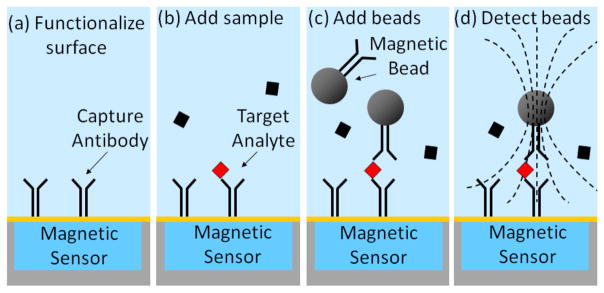
Sandwich immunoassay protocol using magnetic beads as labels. (a) Chip surface is functionalized with capture antibodies specific to the target analyte. (b) Sample is introduced and any target analyte in the sample binds to the surface via the capture antibodies. (c) Magnetic bead labels are introduced; they bind to the surface via the bound target analyte. (d) Bound bead are polarized using external magnetic fields and detected with magnetic sensors below the chip surface.
Several types of magnetic detectors, including giant magnetoresistance (GMR) and spin-valve sensors [5]–[8], inductors [9], and Hall-effect sensors [2], [10]–[19], have been used to detect the magnetic beads. GMR sensors offer excellent sensitivity but usually require an external magnet and are not available in a standard CMOS processes. On-chip inductive sensors offer good sensitivity by utilizing quality-factor amplification but require extensive calibration due to high baseline signals and potential interference from non-magnetic conductors. CMOS-integrated Hall-effect sensors, which are utilized in this work, have relatively poor sensitivity relative to GMR and inductive sensors, but they are not sensitive to conductors and they can be used in conjunction with integrated electromagnets. Further, these sensors can be scaled to several micrometers in size and achieve a signal-to-baseline ratio on the order of 10–100% for magnetic microbeads using relaxation detection techniques [16]–[19]. Hall sensors based on III–V semiconductors can have over ten times the sensitivity of silicon based sensors [11], but they are not available in CMOS processes and would require significant processing overhead to enable sufficiently large detection areas.
One primary difference between standard ELISAs and magnetic label assays is the size of the label. Label size affects label diffusion behavior, binding behavior, and signal strength; changing the size of the label often requires changes in the entire assay protocol and is difficult to analyze beyond experimental means. Small labels, such as enzymes and fluorophores, have dimensions on the order of 5 nm and are widely used in laboratory assays, such as ELISA, respectively. Large labels are much less typical but have the advantage of being easily manipulated via electromagnetic or hydrodynamic forces to enable mixing and to accelerate label sedimentation to the sensor surface, resulting in a faster assay protocol and enabling integrated washing [4], [20]. Table I shows a comparison between typical specifications of commercial ELISAs and two published immunoassays utilizing labels on the order of a micrometer in diameter. The two large-label assays are on average twenty times faster than ELISA and have comparable detection limits, indicating that microlabels are especially suitable in situations where a fast assay protocol is important.
TABLE I.
Comparison of ELISA to Assays Utilizing Microbeads as Labels
Using large magnetic labels in conjunction with CMOS-integrated Hall-effect sensors is particularly advantageous since the larger signals from these labels compensate for the low sensitivity of Hall sensors, enabling sufficiently low detection times and energy consumption levels for POC testing. One particular concern with using microbeads is that only tens to hundreds of magnetic labels may constitute a positive signal, whereas in ELISA the label count is in the millions. A result inferred from such a small number of labels may have significant errors caused by binding statistics and label variations. The aim of this work is to analyze and quantify these errors and demonstrate that clinically accurate measurements can be achieved using CMOS-integrated Hall sensors arrays with detection times and energy consumption levels that meet POC requirements.
II. System Performance Analysis
A. Overview
The primary goal of a POC diagnostic assay is to provide an accurate reading of the concentration of the target analyte under certain constraints. While these constraints vary among different applications, in general, the detection component of a POC tester needs to be inexpensive, battery-powered, and take less than one minute for readout. Thus detection area, energy consumption, and readout time are relevant performance metrics that should be minimized during the design process while maintaining a certain level of readout accuracy.
To quantify accuracy, commercial assay kits commonly provide a user with a standard curve describing the relation between the output signal and the analyte concentration, and a coefficient of variation (CV), which is the standard deviation of the output signal divided by the mean output signal of an assay performed several times with the same concentration of the analyte. In general, it is desirable to achieve a 5–20% CV [21] over a dynamic range of several orders of magnitude of analyte concentration. While the CV is largely dependent on and often limited by the biological reagents used, it is important to ensure that the characteristics of the labels and the detection system do not unnecessarily degrade assay accuracy.
Before discussing error sources contributing to the CV, we need to relate the label signal, defined as the total signal from all labels situated on the sensors, to the analyte concentration being measured. In many assays this relationship is non-linear and, in the region between the limit of detection and saturation, can be described by a power law given by
| (1) |
where [A] is the analyte concentration, n is the number of labels on the surface, and the exponent x is typically between 1–3 for published magnetic bead assays [4], [8], [13]. This non-linearity stems from the non-uniformity of binding affinities between individual analyte-antibody pairs and steric effects associated with the analyte and labels [22]. For small CVs, the non-linearity results in the relationship between CV label and CV [A] of
| (2) |
The non-linearity in the standard curve effectively reduces the accuracy. For example, for a square law relation between labels and analyte concentration (i.e., x = 2), a CV label of 10% results in a CV [A] of 20%.
B. Error Sources
Several error sources are present in label detectors that can significantly impact the CV of the label signal. Some, like electronic noise, are present in all detector systems, whereas errors due to label variations, label binding location variations, and the label binding-process are of particular concern in cases where a small number of labels constitute the final signal. Electronic noise stems from thermal noise and flicker noise generated by sensors and detection electronics. It is desirable to keep the flicker noise corner frequency below the measurement bandwidth and to average or integrate the signal to reduce thermal noise to the required level. Label variations come from variations in label size and/or variations in the signal each label generates (e.g., variations in magnetic content for magnetic labels) and have a standard deviation between 10% and 30% for magnetic beads used in this work. Label binding position variations come from location-dependent sensitivity of the detectors and depend on the sensor design, which is discussed in more detail in sections III and IV.
In general, with a proper detector design, sufficient readout time, and suitable labels, the aforementioned error sources can be kept small. However, signal variations from the label binding process pose a fundamental error source in immunoassays. The binding of a capture antibody to its target analyte is a probabilistic event and follows dynamics that are common to all affinity-based biosensors and are known to generate biological shot noise [23]. Since each capture event is approximately independent of the others and since many such events occur, the number of labels bound to the sensor surface can be described by a Poisson distribution, where the standard deviation of the number of labels is equal to the square root of the mean number of labels. This error source is negligible in assays using large amounts of small labels, such as enzymes or fluorophores, but in the case that only tens to hundreds of labels form the final label signal, the error is significant and is further analyzed below.
Given that the number of labels bound to the surface for a particular analyte concentration has mean n, the standard deviation is then and the Poisson distribution CV(CVP ) is . Thus, the minimum number of labels required to achieve a certain CV P is given by
| (3) |
For example, 400 labels are required to achieve a CV P of 5%. This variation can be reduced only by increasing the number of bound labels, which, for a given analyte concentration, requires an increase of the sample volume and detection area.
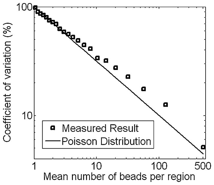
Fig. 2 confirms the above analysis of Poisson error for magnetic bead labels. A magnetic bead immunoassay was performed on a glass substrate using 100 ng/mL of mouse IgG antibodies as the target analyte. The total assay area was divided into multiple, equal-area regions, and the mean, standard deviation, and CV of the number of beads in the regions were calculated. The calculations were then repeated for smaller regions and the CV was plotted versus mean number of beads per region. A close correlation between the measured data and the theoretical Poisson distribution given by (3) can be seen. The experimental results have slightly higher CVs than the theoretical distribution due to other potential sources error, such as non-uniform surface functionalization and non-uniform bead coverage when beads are introduced. Furthermore, approximately 30% of the beads stuck together in clumps of multiple beads due to imperfect assay chemistries, effectively reducing the number of independently binding beads and thus increasing the CV. It is important to note that this analysis effectively treats each region as a separate assay and partially rejects other variations, such as inconsistencies in sample preparation and delivery steps, variations in amounts of biological reagents used, and environmental effects, which would normally occur between different assays and further increase the CV. Thus, the Poisson error sets the lower limit for the CV, and the final CV may be higher due to the aforementioned effects external to the detector system.
Fig. 2.
Graph showing CV versus theoretical and measured mean number of specifically bound beads per region on a glass substrate after an assay was performed.
Now that the error sources have been identified, a formal error analysis may be performed. Let σP, σpos, σsig, σnoise, correspond to the standard deviation due to Poisson error, label binding position variations, label signal variations, and thermal electronic noise, respectively, normalized to the mean signal produced by one label. Assuming the aforementioned error sources are independent and noting that σP = 1, the total CV (i.e., CV label) is given by
| (4) |
where n is the number of labels and N is the total number of sensors forming the detection area. Just like the Poisson error, the errors from label position variations and label signal variations scale with , whereas errors due to electronic noise depend on the total number of sensors and thus are constant for a particular number of sensors and detection time. Assuming electronic noise can be made small by integrating or averaging the sensor signals over a sufficiently long measurement time, the minimum number of labels required to attain a certain CV label and CV [A] is given by:
| (5) |
Recall that x is the exponent in the power law relationship between the number of labels and the analyte concentration, and as expected, (5) reduces to (3) when error sources from label position variations and label variations are negligible. For example, for x = 2 and assuming σpos = 0.3 and σsig = 0.3, which are the approximate values for the sensor array and labels presented in section III, for a CV [A] of 10%, the minimum number of bound labels is n = 435.
C. Minimum Detection Area
The minimum number of labels and the required dynamic range of detection place a constraint on the minimum detection area. The dynamic range (DR[A]), or the ratio of the highest quantifiable concentration to the lowest quantifiable concentration, needs to be between 100 and 10,000 for most immunoassays. Recall that because of the power law relationship in (1), the relationship between the dynamic range of the number of labels (DRlabel) and DR[A] is
| (6) |
For example, if x = 2, a DRlabel of 100 results in a DR[A] of 10,000. The non-linearity of (1) effectively extends the dynamic range of the assay at the cost of decreasing the accuracy (i.e., by increasing the CV).
The minimum detection area can be derived based on (5) and (6). At the lowest quantifiable concentration the assay needs at least n labels to keep Poisson error within a required CV [A], whereas at the highest analyte concentration at least n × DRlabel labels need to be bound to the surface. Assuming that at saturation the surface is approximately fully covered with labels, the required detection area is
| (7) |
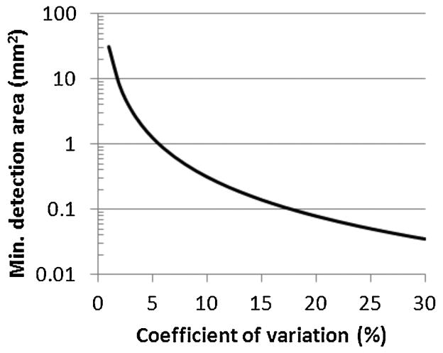
where d is the label diameter. Fig. 3 shows the relationship between detection area A and CV [A] for 2.8 μm diameter labels with x = 2, DR[A] of 10,000, σpos = 0.3, and σsig = 0.3.
Fig. 3.
Minimum detection area for an assay with a DRlabel of 100 utilizing 2.8 μm labels versus desired CV.
Several interesting implications can be derived from (7) and Fig. 3. First, the non-linearity in the standard curve actually helps to reduce the required detection area as the term decreases as x becomes larger for typical values of DR[A]. Second, the detection areas for a high accuracy assays utilizing 2.8 μm labels are on the order of 1 mm2 and are readily attainable on CMOS chips. Labels larger than 10 μm, however, are not suitable for on-chip assays as they would require areas in excess of 10 mm2 just for the sensors, a size that would be impractical due to high chip costs.
The above analysis derives the minimum required detection area as a function of label size and assay accuracy and is not limited to solely magnetic sensors and magnetic labels; it can be applied to any type of sensor or sensor array designed to detect labels, for example, fluorescent or colored beads in conjunction with optical detectors [24]–[26]. Since it is desirable to keep the detection area as small as possible, the errors from non-Poisson error sources should be made smaller or equal to the Poisson error during the design and detection processes. Additionally, the detection time and energy should also be minimized, which, for many sensor types, is most effectively achieved by maximizing the signal detected by each sensor. The next section will apply the analysis provided here to the design and optimization of Hall-effect sensors for the detection of magnetic bead labels.
III. Bead Detector Design
A. Overview
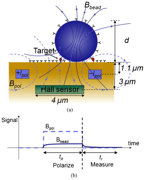
Fig. 4(a) shows a cross section of a CMOS-integrated Hall-effect bead detector and Fig. 4(b) shows the detection method used in this work. A Hall sensor having a length of 4 μm is located at a distance 3 μm below the chip surface. Since magnetic beads are paramagnetic, they need to be polarized by an external field prior to detection. In order to obviate large, high-power external electromagnets, the polarization field generator is integrated on-chip [14]. Wires located at a distance of 1.1 μm below the surface carry an alternating current (+I pol, −I pol) to generate a magnetic field (Bpol) that polarizes the magnetic beads. The polarized bead creates an induced magnetic field, Bbead, that is well modeled by a simple dipole [2] located at a height 3 μm + d/2 above the sensor, where d is the bead diameter. After polarizing the bead for time tp, Bpol is abruptly turned off, leaving a remnant Bbead that relaxes while being measured over time tr. The polarization and measurement steps are repeated many times to reduce thermal noise and correlated double sampling is used to reject flicker noise [17]–[19]. The Hall sensor, which is sensitive to magnetic fields orthogonal to the sensor surface, converts Bbead into an alternating voltage signal of magnitude VH, which appears across two sense contacts placed on opposite sides of the Hall sensor. For the beads used in this work, the detection performance, defined as the total signal-to-noise ratio (SNR) per total measurement time (Tm), has a shallow optimum for polarization frequencies in the range of 1–10 MHz [16], [19]. A polarization frequency of 2 MHz, corresponding to a tp and tr of 125 ns, was chosen and is above the measured 1/f noise corner frequency of 830 kHz [19].
Fig. 4.
(a) Cross-section of a Hall-effect bead detector showing the relevant magnetic fields. (b) Detection method based on magnetic relaxation.
As discussed in the previous section, detection areas on the order of 1 mm2 are required when using microbeads as labels. Unfortunately, millimeter-sized Hall sensors are not sufficiently sensitive to detect hundreds of magnetic beads without resorting to impractically lengthy signal averaging times and complex calibration steps. Although there is considerable local magnetic field arising from a magnetic dipole moment of a single bead, the total magnetic field integrated over the plane of the Hall sensor approaches zero as the plane becomes larger since magnetic field lines always form a closed curve [2]. Only a small Hall sensor can capture the local magnetic field lines from a dipole before they reverse direction. Consequently, large arrays of micrometer-sized Hall sensors are needed to achieve a sufficient detection area for bead quantification. An array implementation is also preferred for polarization field generators as they need to be in close proximity to magnetic beads since magnetic fields from current carrying wires are inversely proportional to distance.
B. Post-Processing
The magnitude of Bbead is asymptotically proportional to the inverse of the cube of the distance between the bead center and the sensor. Thus one of the primary design optimizations is to make this distance as small as possible. In the sensor arrays presented here, the distance between the surface and sensors was reduced from 9 μm to 3 μm by etching of the inter-layer dielectric (ILD) above the sensor area, which results in a 10x – 20x signal strength increase for bead sizes on the order of 1 μm.
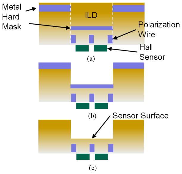
Fig. 5 shows the post-processing flow [15]. Metallization layers, fabricated as part of the CMOS process, were used as a hard mask for the reactive-ion etching of the ILD. Although etching was performed after the CMOS process was completed, this etch step can be readily integrated into the CMOS process by simply lengthening the time of the final passivation etch used to expose the pads. A metal wet etch, which is optional, was performed after the ILD etch to remove the metal hard mask, which brings the beads another 0.5 μm closer to the Hall sensor array. An optional dip in standard clean solution (5:1:1 ratio of H2O, H2O2, and NH3OH) removed the Ti/TiN liner and made the sensors optically visible. After the post-processing is completed, only one metal layer and one polysilicon layer remain for routing signals in the detection area, restricting the architecture of the polarization field generator and the sensor cell to only these two routing layers.
Fig. 5.
Etching steps performed after CMOS chip fabrication to reduce distance between beads and Hall sensors. (a) Chip is fabricated with a metal hard mask defining the sensor region. (b) RIE etch is used to remove ILD over the sensor region. (c) Exposed metal layer over sensor surface is removed with a wet etch.
C. Sensor Array Architecture
The magnetic moment induced on a bead is proportional to the external field Bpol. As a result, placing polarization wires in close proximity of the bead and increasing I pol results in a larger magnetic moment and, larger signal. The ability to place polarization field generators within several micrometers of the label is a critical advantage of fully integrated detectors over ones that resort to external magnets, which typically consume on the order of a 1 W of power [27].
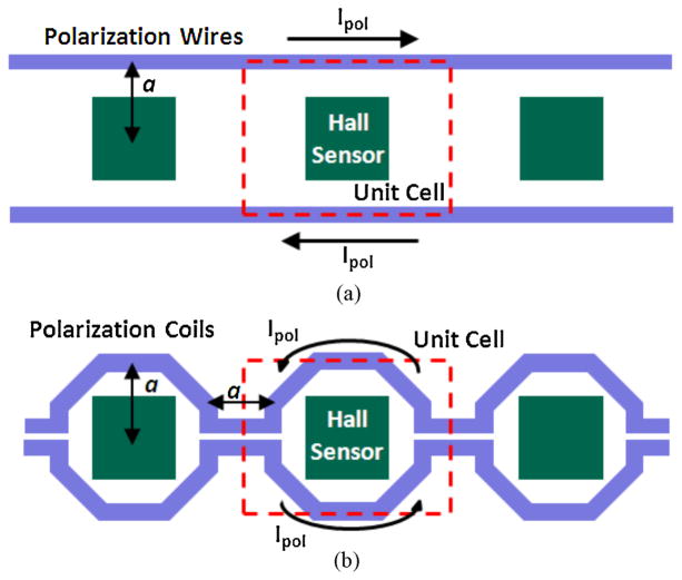
Both integrated wires and micro-coils (Fig. 6) can be used as field generators. Simulations were performed to compare the average bead signal generated by each architecture for the same sensor pitch a. It was found that the average signals from the different architectures are within 20% of the other for bead sizes between 100 nm and 5 μm, with microcoils slightly better for beads below 2 μm in diameter and wires better for beads above 2 μm in diameter. Since wires provide a simpler, more compact layout, and smaller voltage drop per row length, the wire architecture is preferable and was used in the array implementations presented here.
Fig. 6.
Two polarization field generator architectures based on (a) Polarization wires. (b) Polarization coils.
Under a uniform out-of-plane magnetic field B, the Hall voltage signal from a Hall-effect sensor, VH, is given by
| (8) |
L where W and L are the width and length of the Hall plate, respectively, G is a geometric factor between 0 and 1, μH is the hall mobility of the Hall plate and Vbias is the bias voltage across the hall plate. In general, should be set between 0.66 and 1 as in this range the product G is the largest and approximately 0.6 [28].
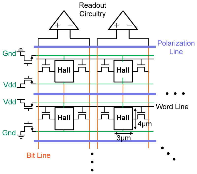
Hall sensors were implemented using an n-well due to its relatively high mobility and sufficient packing density [15]. Fig. 7 shows the architecture of the sensor array showing four sensor unit cells. Each unit cell contains a Hall plate, supply lines (V dd and GND), polarization lines, signal bit lines, and a digital word line that connects to access transistors similar to those in static random-access memory (SRAM). The size of each sensor was chosen to be 3 μm wide and 4 μm long since each dimension is similar to the distance from the sensor to the bead center and thus efficiently captures magnetic field lines from the bead. Larger Hall sensors generate a substantially smaller signal whereas smaller Hall sensors are difficult to implement in the CMOS process used in this work and generate only modest signal gains at the cost of higher sensor offset and larger signal variations. Since the signal strength is proportional to V bias and doubling the signal reduces the averaging time by a factor of four and energy consumed by a factor of two, V bias should be maximized and was set equal to the supply voltage V dd = 2 V, close to the maximum voltage for this process technology.
Fig. 7.
Hall-effect sensor array architecture.
Continuing with Fig. 7, switches at the sides of the array connect the sensor terminals of one row to the supply lines while another set of switches (not shown) turn on the current running through polarization lines next to the enabled sensors to polarize beads in their vicinity. The supply lines and polarization lines are shared between adjacent rows to minimize voltage drop and the polarization current is routed to another array bank during the relaxation phase shown in Fig. 4(b) to save time and energy. The word line is enabled to transfer sensor signal to the bit-lines that carry the signals to the top and bottom of the array to be digitized in parallel by a series of pitch-matched amplifiers and digitizers [18], [19]. The array can be scaled by utilizing multiple array banks or by introducing more rows up to a limit of 64 due to thermal noise arising from the high resistance poly bit lines. The main design problem thus lies in designing the individual row of sensors that makes up the array.
D. Sensor Array Design and Optimization
After selecting a sensor size, the two primary degrees of freedom that remain in designing the sensor array are the number of sensors per row, N row, and the polarization current, I pol. As N row is made larger, more sensors are polarized and read out in parallel and thus the detector array is faster and more energy efficient. Unfortunately, metal lines have finite resistivity, so as N row is made larger, the widths of polarization lines and the supply lines need to be scaled to maintain a suitably low voltage drop. Wide lines effectively add area overhead to the sensor unit-cell by creating regions in the unit-cell where beads are far away from Hall sensors, resulting in a small signal in those regions. Consequently, the mean bead signal drops and bead location error σpos increases, eventually decreasing performance despite the parallelization benefit.
Consider next the choice of the polarization current Ipol. The detector total current consumption can be written as
| (9) |
where Isens is the current due to the Hall sensors and Ireadout is the current due to the readout circuitry. In most cases, doubling Ipol doubles the bead signal, and, therefore, reduces measurement time by a factor of four in the case thermal noise dominates, as is the case for the detectors presented here. At the same time, power consumption increases by less than two times and, therefore, energy consumption is reduced by more than two fold. The maximum I pol that may be used is nevertheless limited by three effects:
First, as in the case of increasing N row, the polarization wire width must be increased with increasing I pol, eventually leading to reduced performance for the same reasons as described above for scaling N row.
Second, there is a critical magnetic field Bcrit, such that for fields larger than Bcrit, the relationship between polarization field and bead magnetic moment becomes substantially nonlinear and the bead signal begins to saturate. Increasing the polarization field beyond Bcrit provides incremental improvements in the signal strength and eventually degrades energy consumption. Bcrit was measured for several beads and is on the order of 3–10 mT [5], [29], which roughly corresponds to I pol values of 64 mA to 256 mA in the sensor arrays implemented in this work.
Third, device heating may become problematic with increasing current. The total temperature at the surface of the chip comes from global heating of the entire system (i.e., chip, fluid, and printed-circuit-board) over the time a measurement is performed and from local heating just above a polarization line that is turned on. Thermal simulations show that localized heating dominates and global heating can be kept substantially lower with standard printed circuit board (PCB) packaging techniques. Polarization wires carry large currents and are not connected to the silicon substrate at any point within the array, contributing most of the surface temperature rise of the chip. Proteins and protein-to-protein bonds degrade rapidly at temperatures above 60–70°C [30], [31]. Although detection takes place after the other assay steps are already performed, total surface heating over 20–30°C may denature antibodies in seconds and may substantially weaken antibody-antigen binding forces, potentially breaking specific bonds and causing beads to move away from the sensors to skew the signal.
To find the optimal sensor array structure, the array was simulated for a range of values N row and I pol to obtain the detection time, energy dissipated, and detection area for each array instance. Effects of magnetic field saturation were ignored for this simulation and were found to be negligible in section IV. For this particular example, a Poisson CV of CV P = 5% was chosen along with a dynamic range of DRlabel = 100, which at the lowest detectable concentration, corresponds to 400 beads covering 1% of the array. The mean signal and label position error σpos were calculated using a finite element method (FEM) simulator that was verified experimentally [15]. Total time was computed such that the total thermal noise CV was set equal to the Poisson error CV (i.e., CV noise = CV P = 5%), which resulted in an approximately optimal performance yielding a final CV label of 7.4%. Energy was computed by taking the product of the time and the average power dissipated. Finally, since time, energy, and area are important parameters for a POC system, the figure-of-merit (FOM) was chosen to be:
| (10) |
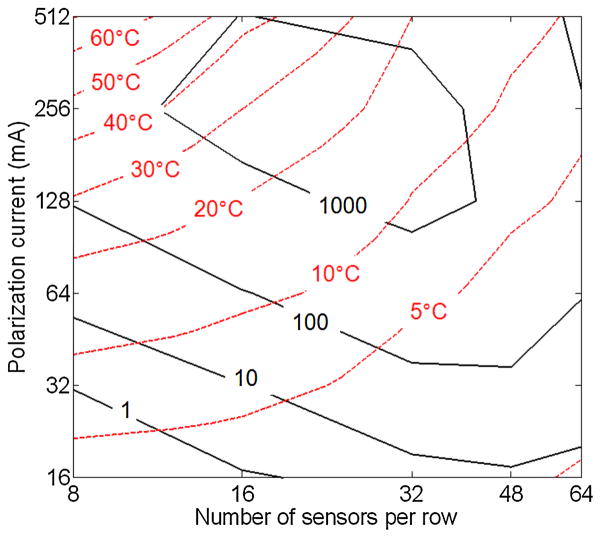
Fig. 8 shows a graph of the FOM (black contours) for different array instances having different values of I pol and N row. The optimal range lies for I pol between 128 mA and 512 mA, and N row between 16 and 48. At low I pol and N row, the signal is small and the array does not take advantage of potential parallelization. At high I pol and N row, the wiring overhead is so large that the average signal drops and position-dependent error increases beyond the Poisson error, reducing the performance.
Fig. 8.
Contour plots of FOM and maximum surface temperature rise for various values of polarization current and number of sensors per row.
The optimal currents suggested above are relatively high and cause substantial surface temperature rise. In order to quantitatively characterize the surface heating, thermal FEM simulations were performed by modeling the sensor row as an infinitely long structure. The maximum surface temperature is overlaid on Fig. 8 (red contours). In general, the more current is used the more heat is generated, whereas the smaller the N row is made, the narrower the polarization lines become and the less efficiently the heat is transferred to the silicon substrate, resulting in a larger temperature rise. The simulation shows that at I pol = 128 mA and N row = 32 the FOM is within 30% of the maximum value and heating is below 10°C, yielding a good safety margin from a maximum rise of 20°C, and, hence, this is the preferred point of operation.
IV. Results
A. Sensor Characterization
Two test arrays were implemented and measured to characterize the Hall sensors: one with rows of sensors designed for I pol = 32 mA and N row = 32 and one for row of sensors designed for I pol = 128 mA and N row = 32. Each sensor row implementation was tested using 4.5 μm M450 beads as they can be positioned accurately using a micromanipulator. Table II lists several parameters and measurement results obtained for each Hall sensor implementation. The 128 mA sensors were measured up to 106 mA due to current routing limitations. Since no degradation of signal due to bead signal saturation or temperature rise was seen, the results of the 106 mA measurement were extrapolated to I pol = 128 mA. The 128 mA polarization wires generate 3.2 times larger signals than those generated by the 32 mA polarization wires. Sensor sensitivity was measured by measuring sensor response to the vertical component of the polarization field Bpol, which itself was calculated using Ampere’s law from I pol. The off-center bead signal was simulated across the sensor surface and the simulations were verified by measuring beads at the top, bottom, and corner of each unit-cell [15]. Despite the substantially wider polarization lines needed to deliver a 128 mA polarization current, bead signals are still relatively uniform within the 128 mA sensor unit cell with a σpos of 0.20 for 4.5 μm beads and σpos of 0.47 for 1 μm beads. Even in the worst case of σpos = 0.47, a 5% CV label due to Poisson error would be increased by (12 + 0.472)1/2 = 10% to get a CV label of 5.5%, which is a relatively small increase in error. Thermal noise spectral density was found to be 260 nT/Hz1/2.
TABLE II.
Summary of Sensor Parameters for 32 mA Sensors and 128 mA Sensors. Optical Images and Sensitivity Heat Maps for Each Implementation are Also Shown for 4.5 μm Beads
| Parameter | 32 mA sensor | 128 mA sensor |
|---|---|---|
| Polarization current Ipol (mA) | 32 | 128 |
| Width of polarization lines (μm) | 1.6 | 6 |
| Width of supply lines (μm) | 1 | 1 |
| Unit-cell dimensions, width by height (μm) | 8 by 7.9 | 8 by 12.3 |
| Max. vertical polarization field (mT) | 3 | 9.6 |
| Max. field from 4.5 μm bead (μT) | 17 | 53 |
| Bias voltage (V) | 2 | 2 |
| Sensitivity (V/V/T) | 0.025 | 0.025 |
| Max. Hall voltage from 4.5 μm bead (μV) | 0.85 | 2.7 |
| Noise spectral density (nT/Hz1/2) | 260 | 260 |
| Label pos. error σpos for 4.5 μm beads | 0.13 | 0.20 |
| Label pos. error σpos for 2.8 μm beads | 0.27 | 0.37 |
| Label pos. error σpos for 1 μm beads | 0.34 | 0.47 |
| Top-view optical image of sensor unit-cell (left) and corresponding sensitivity heat map (i.e., relative signal from a bead that lands in the corresponding position). |

|

|
Sensitivity variations between different sensors in the array were measured to have a standard deviation of 1.4%, adding negligible signal error. To evaluate the variations in beads (σsig), signals from several individual 2.8 μm and 4.5 μm beads were measured and the standard deviation was computed to be σsig = 0.096 for 4.5 μm beads and σsig = 0.31 for 2.8 μm, in both cases much smaller than the Poisson error, indicating that variations in these labels do not substantially degrade accuracy.
B. Array Characterization
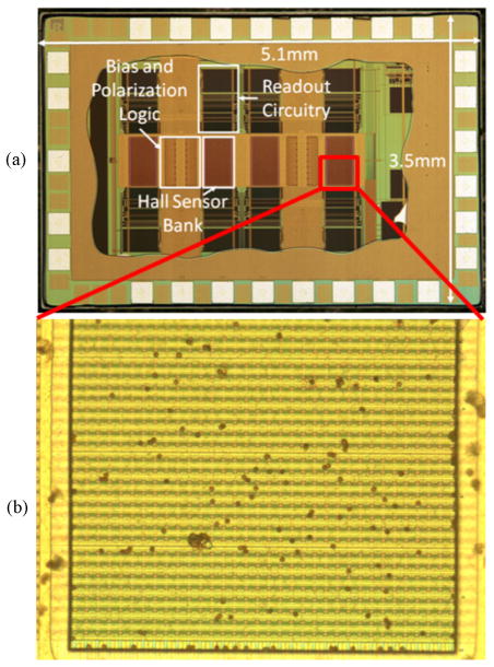
A large Hall-effect sensor array was designed and implemented for quantifying microbeads on its surface with high accuracy. The detection area was chosen based on (7) for 2.8 μm beads, a DRlabel of 100, and CV label of 5%, which, for a power law relationship of (1) with x = 2, gives assay parameters of DR[A] = 10,000 and CV label = 10%. A minimum number of n = 400 beads is required to overcome Poisson error and a maximum number of n × DRlabel = 40,000 beads need to be fitted within the detection area, which evaluates to 0.31 mm2. We designed and implemented an 8192-sensor array that has a detection area of 0.52 mm2 [18], [19] to meet these specifications. In order to ensure robust operation, this version of the array was designed for a current I pol = 32 mA array and has 32 active sensors per row (N row = 32). The array consists of 4 banks of 2048 active sensors each and is shown in Fig. 9.
Fig. 9.
(a) Optical image of the sensor chip containing 4 banks with 2048 active sensors each. (b) One half of a 2048 Hall sensor array bank with M280 beads covering approximately 2% of the surface.
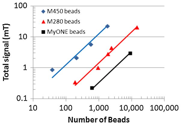
For the sensor array to function as bead detector, it must display a known and preferably linear transfer function between the number of beads on the array and the sum of the signals of all sensors in the array. Fig. 10 shows the relationship between the number of beads placed on the array versus the total relaxation signal obtained from the sensors in the array for three different beads, 4.5 μm M450, 2.8 μm M280, and 1 μm MyOne beads from Invitrogen Corp. Two of the array banks and a total of 4096 sensors, spanning approximately 0.26 mm2, were used to perform this measurement. The response is linear with R > 0.99 for all three bead types, and one 4.5 μm bead produces an eight times and 20 times greater signal than one 2.8 μm and one 1 μm bead, respectively.
Fig. 10.
Sum of all bead signals from all sensors versus number of beads placed on the array for the 32 mA sensor array architecture and measurement parameters presented in Table II.
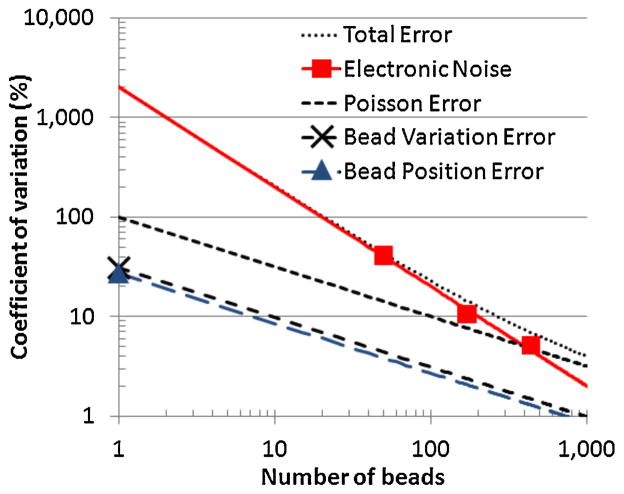
Fig. 11 depicts errors from various sources, including the expected Poisson error and the measured thermal noise, as a function of the number of beads on the array. The CV due to thermal noise decreases with the inverse of the number of beads since the total signal directly increases while thermal noise stays constant. Bead signal variations, bead position variations, and Poisson error increase in an uncorrelated fashion as the number of beads increases; consequently their CVs decrease with the inverse of the square root of the number of beads. Since these errors are approximately independent, the total error CV is the root mean square value of all the errors. The measured values for a single bead for bead position variations and bead variations derived above are indicated as points in Fig. 11. To verify that the array can make accurate measurements, three experiments with 50, 170, and 440 beads placed on the array, respectively, were performed by measuring the total signal several times and calculating the CV of the measured signals. Each measurement took 480 ms per sensor and 30 s for the entire array. For the case of 440 beads, which corresponds to approximately 1% bead coverage of the array and is essentially the worst case dynamic range (i.e., 100), this array was designed for the error due to thermal noise results in a CV of 5.3% and the total error has a CV of 7.4%. At 440 beads, only 0.3% of the 7.4% error is contributed from bead variations σsig and from bead position variations σpos; consequently these errors are insignificant compared to the Poisson and thermal noise errors.
Fig. 11.
Coefficient of variation versus number of beads 2.8 μm beads placed on the array for various error sources. Points indicate measured results and lines indicate simulated or calculated values. Thermal noise CV error is given for a measurement time of 480 ms per sensor (30 s for the entire array).
Based on the measured signal values for each of the beads and the measured thermal noise of the array, the detection time, energy, and the required area to achieve a CV P = CV noise = 5% = > CV label = 7.1% and DRlabel = 100 are derived for M450, M280, and MyOne beads and are shown in Table III. Larger beads require larger areas but generate larger signals, thus requiring a shorter measurement. For all the beads the detection times are below one minute and the energy requirements are well below those supplied by small batteries. Interestingly, MyOne beads have the highest FOM since they require a comparably small detection area while generating a relatively large signal due to a high magnetic content and the fact that their bead centers are closer to the Hall sensors than those of the larger beads.
TABLE III.
Time, Energy, Required Detection Area, and FOM for Various Bead Sizes Required to Obtain a CVlabel = 7.1% and DR = 100 for a Hall Sensor Array Implementation With Ipol = 32 mA and Nrow = 32
| Bead | Area | Time | Energy | FOM |
|---|---|---|---|---|
|
| ||||
| M450® | 0.81 mm2 | 8.5 s | 1.3 J | 320 |
| M280® | 0.34 mm2 | 40 s | 6.2 J | 35 |
| MyOne® | 0.045 mm2 | 13 s | 2.1 J | 2,500 |
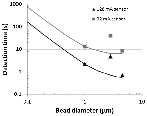
Fig. 12 shows the detection time versus bead size of the three types of beads measured in Fig. 10 for a CV label = 5% and a DRlabel = 100, equivalent to 400 beads covering 1% of a sensor array, for both a 32 mA sensor architecture and a 128 mA sensor architecture. The detection time is also extrapolated (solid lines) for all beads between 100 nm and 4.5 μm diameter from the measured signal of the 1 μm MyOne bead. The 2.8 μm beads fit the solid curve poorly due to their substantially lower magnetic content per volume (12% for 2.8 μm beads versus 26% for 1 μm beads) and thus result in a lower than expected signal and larger than expected measurement time. For the array architecture having I pol = 32 mA and N row = 32, magnetic beads having a diameter of 500 nm can be accurately detected in less than one minute. The results are further extrapolated to an architecture based on 128 mA polarization currents measured in Table II. Using the 128 mA architecture, microbeads can be quantified within 5 seconds and 200 nm beads can be accurately quantified in less than one minute. Beads larger than 4.5 μm provide little signal gain since their centers become significantly far removed from the polarization lines and Hall sensors, diminishing the signal.
Fig. 12.
Required detection time to achieve a CVlabel of 7.4% and DRlabel of 100 versus bead diameter for sensor types in Table II. The points show values from Table III for 1 μm, 2.8 μm, and 4.5 μm Dynal beads while solid lines extrapolate detection time to other bead sizes based on the magnetic density of the 1 μm Dynal bead.
C. Signal Demodulation Using Thresholding
In the analyses and measurements presented above, the total array signal is obtained by summing the signals from the individual Hall sensors. This method has a drawback in that uncorrelated thermal noise from all the sensors in the array is also added together, doubling the total noise voltage every time the array is made four times larger. Measurement times for each individual sensor can be increased to counter this effect, but this increases the total detection time, which is limited to one minute for POC applications. Because of this addition of noise, the dynamic range for microbead labels on the Hall sensor array presented here is limited to about DRlabel = 100–300, corresponding to 0.3–1% bead area coverage. While this range is sufficient for many assay applications, in some assays, especially those where there is a linear or nearly linear relationship between the number of magnetic labels and the analyte concentration [20], a larger dynamic range is preferred.
An alternative method for demodulating the signal can be used with this architecture. Since microbeads generate relatively large, spatially concentrated signals, a single bead positioned over a 3 μm by 4 μm Hall sensor can be detected with an SNR of 20 dB in less than 100 ms [17]. Since, at low bead concentrations, it is unlikely that two or more beads bind to the surface of a single sensor, a single threshold level can be used to decide whether a bead lies above the sensor or not. At SNR of 20 dB, false positive and false negative decisions for beads positioned in the center of a sensor occur with a probability less than 1 in 1 million, enabling very large dynamic ranges. These individual decisions can then be added up in the digital domain without adding up noise.
Despite the clear advantages, thresholding demodulation has several drawbacks specific to Hall sensor arrays. First, bead signals vary with position over a sensor and no matter what value a threshold is set to, a bead may land in a position where its signal is close to the threshold, producing a large variance in decisions in the presence of thermal noise. Second, beads landing in between two sensors, which are still partially counted using summing demodulation, will not be detected for thresholding demodulation using reasonable thresholds, effectively decreasing the total array signal and increasing position dependent error σpos.
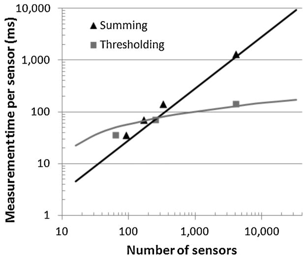
To quantify the performance of thresholding demodulation versus summing demodulation, an experiment using 13 M450 beads placed on the 4096 sensor array was performed. Each sensor was measured for 35 ms, 70 ms, 140 ms, and 1120 ms, generating an SNR per bead of 14 dB, 17 dB, 20 dB, and 29 dB, respectively. As in the experiment in reference to Fig. 11, measurements for the whole array were repeated multiple times to collect statistical information. The bit error rate (BER) of a bead placed in a random position on the sensor unit cell using the aforementioned SNR values was simulated and a threshold level that minimizes the CV was empirically found. This threshold level was then used to count the beads for experimental measurement using thresholding detection. A CV noise of 15% was achieved for the thresholding demodulation for the 140 ms per sensor measurement time whereas for summing demodulation the CV noise was measured to be 55%, nearly four times larger. To depict how thresholding modulation allows for scaling a sensor array to a large number of sensors, the results of the experiment are presented in Fig. 13 where the horizontal axis is the number of sensors and the vertical axis is converted into the required measurement time per sensor to obtain a CV noise of 15%. The points represent measured results and the solid lines represent the expected value from the statistical simulations. To measure effectively less than the 4096 sensors of the array, for each measurement the sensors under and in the vicinity of the 13 beads were measured and a variable amount of additional sensors were also measured, simulating a variable size array. As more sensors are added, more noise is added to the signal and proportionally more averaging time per sensor is required for summing demodulation to obtain a constant CV noise. For thresholding, the required time also initially increases approximately linearly as bit errors proportionally decrease with extra measurement time for low SNR values. However, as measurement time increases and SNR approaches 20 dB, bit errors become very rare and the additional measurement time per additional sensor added to the array becomes sub-linear. The 13 beads, covering only 0.1% area of the array, are detected in 9 s total using the thresholding detection method. Extrapolating this result shows that an array with 30,000 sensors can readout 13 beads in 60 s with a CV noise of 15% (assuming N row = 32), showing that the thresholding technique can achieve dynamic ranges in excess of DRlabel = 5000.
Fig. 13.
Measurement time per sensor required to quantify 13 beads with CVnoise of 15% versus number of sensors in the array for summing and thresholding demodulation methods.
V. Conclusion
Magnetic beads are excellent candidates as labels for biological assays that are performed on integrated platforms. We demonstrated that magnetic bead labels on the order of 1 μm in diameter can be quantified with accuracies sufficient for biological assays in detection areas small enough to fit on CMOS chips and with a detection time and energy requirements suitable for POC settings. A 0.26 mm2 Hall-sensor array implemented in a 0.18 μm CMOS process can quantify a 1% surface coverage of magnetic microbeads with a worst case CV of 7.4% within 1 minute while dissipating less than 10 J of energy, less than 0.1% of the energy stored on a typical smartphone battery. Utilizing thresholding demodulation, a feature of this implementation due to the inherent array design, beads covering only 0.1% of the detection area were detected in just a few seconds with high accuracy. Thus robust and compact detection platforms based on CMOS Hall-effect sensors and magnetic microbead labels are suitable as detectors for high accuracy point-of-care assays.
Acknowledgments
This work was supported by the trans-NIH Genes, Environment and Health Initiative, Biological Response Indicators of Environmental Systems Center, under Grant U54 ES 016115-01.
Biographies

Karl Skucha received the B.S. and M.S. degrees in electrical engineering and the Ph.D. degree from the University of California, Berkeley, CA, USA, in 2006, 2009, and 2012, respectively. He was an Intel Robert Noyce fellow and his doctoral work was focused on CMOS-integrated magnetic particle detectors for diagnostic applications.

Simone Gambini received the Laurea Specialistica degree from University of Pisa and Sant’Anna School of Advanced Studies, Pisa, Italy, in 2004, and the Ph.D. degree in electrical engineering from the University of California, Berkeley, CA, USA, in 2009. His doctoral research was developed at the Berkeley Wireless Research Center and was partially funded by an Intel fellowship.
In 2010, he was with Telegent Systems, where he designed RF circuits for highly integrated mobile TV tuners. From 2011 to 2012, he was affiliated with the Berkeley Sensor and Actuator Center, where he conducted research on biosensors and MEMS interfaces. He is currently a Lecturer with the Electrical Engineering Department of the University of Melbourne, Parkville, Australia. His current research interests include the application of low-power electronics to create microsystems integrating sensing and communication, and the development of circuit design techniques for post-CMOS devices.

Paul Peng Liu received the B.S. degree in microelectronics from Peking University, Beijing, China, the M.S. degree in electrical engineering from North Carolina University, and the Ph.D. degree in electrical engineering from the University of California, Berkeley, CA, USA.
Prior to joining Berkeley in 2007, he was a Staff Design Engineer with Xilinx Inc. working on high-speed serial link transceivers. His current research interests include CMOS/MEMS sensors and analog/mixed-signal integrated circuit design.

Mischa Megens received the Ph.D. degree in physics from the Van der Waals-Zeeman Institute, University of Amsterdam, The Netherlands, in 1999.
In 2001, he joined Philips Research, where he worked in such diverse fields as biosensors for point-of-care diagnostics, GaN photonic crystal LED light extraction, soft imprint lithography, polymer OLEDs, electrowetting-based beam steering, and ultrasound for cardiac ablation monitoring. He is currently a Senior Research Scientist with the University of California, Berkeley, CA, USA, where he is currently working on high-speed optical beam steering using phased arrays of lightweight high-contrast grating mirrors.

Jungkyu Kim is an Assistant Professor of mechanical engineering at Texas Tech University, Lubbock, TX, USA. His research expertise includes lab-on-a chip devices that require a variety of microfluidic components for complex chemical/biomedical assays. His work has involved the development of microfluidic control systems, microfluidic sample processing, nucleic acid sample preparation and on-chip amplification, protein microarrays, CNT biosensors, and immunomagnetic detection. At UC Berkeley, he conducted research in microsystems for carcinogen detection from human blood, development of 3-D hydrogel-based microarrays, and point-of-care devices for TB detection. Prior to that, at the Center of Excellence for Biomedical Microfluidics at the University of Utah, he conducted research in carbon nanotube based lab-on-a-chip development for water safety, development of biochips for personalized medicine, and integrated microfluidic systems. He has authored or coauthored more than 50 peer-reviewed journal and conference publications, one book chapter, and eight patents issued or pending in the area of microfluidics, biosensors, and cell/tissue engineering. He has been a recipient of numerous awards, including the Best Paper Award from the Korea Orthopedic Research Society, the National Research Foundation fellowship, and the Pierre-Lassonde entrepreneur fellowship.

Bernhard Boser (F’03) received the Ph.D. degree from Stanford University, Stanford, CA, USA, in 1988.
He was a member of Technical Staff with Bell Laboratories. In 1992, he joined the faculty of the Electrical Engineering and Computer Science Department, University of California, Berkeley, CA, USA. His current research interests include the area of analog and mixed signal circuits, with special emphasis on ADCs and micromechanical sensors and actuators.
Dr. Boser has served on the program committees of ISSCC, VLSI Symposium, Transducers, and was the President of the IEEE Solid-State Circuits Society. He is a co-founder of SiTime, a fabless semiconductor company.
Contributor Information
K. Skucha, Email: kskucha@eecs.berkeley.edu, Electrical Engineering Department, University of California, Berkeley, CA 94720 USA
S. Gambini, Email: sssimone@eecs.berkeley.edu, Electrical and Electronic Engineering Department, University of Melbourne, Parkville, Vic. 3010, Australia
P. Liu, Email: paulliu99@gmail.com, Microsensor Labs, Chicago, IL 60629 USA
M. Megens, Email: megens@eecs.berkeley.edu, Electrical Engineering Department, University of California, Berkeley, CA 94720 USA
J. Kim, Email: jungkyu.kim@berkeley.edu, Mechanical Engineering Department, Texas Tech University, Lubbock, TX 79401 USA
BE Boser, Email: boser@eecs.berkeley.edu, Electrical Engineering Department, University of California, Berkeley, CA 94720 USA.
References
- 1.Myers F, Lee L. Innovations in optical microfluidic technologies for point-of-care diagnostics. Lab Chip. 2008 Dec;8(12):2015–2031. doi: 10.1039/b812343h. [DOI] [PubMed] [Google Scholar]
- 2.Aytur T, Anwar M, Ishikawa T, Beatty PR, Boser BE. An immunoassay platform based on CMOS Hall sensors. Proc. Dig. Tech. Papers Solid-State Sensors Actuators Microsyst. Workshop; Jun. 2002; pp. 126–129. [Google Scholar]
- 3.Florescu O, Wang K, Au P, Tang J, Harris E, Beatty PR, Boser BE. On-chip magnetic separation of superparamagnetic beads for integrated molecular analysis. J Appl Phys. 2010 Mar;107(5):054702. doi: 10.1063/1.3272779. [DOI] [PMC free article] [PubMed] [Google Scholar]
- 4.Kim J, Jensen E, Megens M, Boser BE, Mathies R. Integrated microfluidic processor for solid phase capture immunoassays. Lab Chip. 2011 Jul;11(18):3106–3112. doi: 10.1039/c1lc20407f. [DOI] [PubMed] [Google Scholar]
- 5.Baselt D, Lee G, Natesan M, Metzger S, Sheehan P, Colton R. A biosensor based on magnetoresistance technology. Biosens Bioelectron. 1998 Dec;13(7–8):731–739. doi: 10.1016/s0956-5663(98)00037-2. [DOI] [PubMed] [Google Scholar]
- 6.Ferreira H, Graham D, Freitas P, Cabral J. Biodetection using magnetically labeled biomolecules and arrays of spin valve sensors. J Appl Phys. 2003 May;93(10):7281–7286. [Google Scholar]
- 7.Rife J, Miller M, Sheehan P, Tamanaha C, Tondra M, Whitman L. Design and performance of GMR sensors for the detection of magnetic microbeads in biosensors. Sensor Actuators A-, Phys. 2003 Nov;107(3):209–218. [Google Scholar]
- 8.Gaster R, Hall D, Nielsen C, Osterfeld S, Yu H, Mach K, Wilson R, Murmann B, Laio J, Gambhir S, Wang S. Matrix-insensitive protein assays push the limits of biosensors in medicine. Nature Medicine. 2009 Oct;15:1327–1332. doi: 10.1038/nm.2032. [DOI] [PMC free article] [PubMed] [Google Scholar]
- 9.Wang H, Chen Y, Hassibi A, Scherer A, Hajimiri A. A frequency-shift CMOS magnetic biosensor array with single-bead sensitivity and no external magnet. Proc. ISSCC Dig. Tech. Papers; Feb. 2009; p. 438. [Google Scholar]
- 10.Besse P, Boero G, Demierre M, Pott V, Popovic R. Detection of a single magnetic microbead using a miniaturized silicon Hall sensor. Appl Phys Lett. 2002 Jun;80(22):4199–4201. [Google Scholar]
- 11.Mihajlovic G, Xiong P, von Molńar S, Ohtani K, Ohno H, Field M, Sullivan G. Detection of single magnetic bead for biological applications using an InAs quantum-well micro-Hall sensor. Appl Phys Lett. 2009 May;87(11):112502. [Google Scholar]
- 12.Sandhu A, Kumagai Y, Lapicki A, Sakamoto S, Abe M, Handa H. High efficiency Hall effect micro-biosensor platform for detection of magnetically labeled biomolecules. Biosens Bioelectron. 2006 Sep;22(9):2115–2120. doi: 10.1016/j.bios.2006.09.021. [DOI] [PubMed] [Google Scholar]
- 13.Aytur T, Foley J, Anwar M, Boser BE, Harris E, Beatty PR. A novel magnetic bead bioassay platform using microchip-based sensors for infectious disease diagnosis. J Immunol Meth. 2006 Jul;314(1–2):21–29. doi: 10.1016/j.jim.2006.05.006. [DOI] [PubMed] [Google Scholar]
- 14.Florescu O, Mattman M, Boser BE. Fully integrated detection of single magnetic beads in complementary metal-oxide-semiconductor. J Appl Phys. 2008 Feb;103(4):046101. [Google Scholar]
- 15.Skucha K, Liu P, Megens M, Kim J, Boser BE. A compact Hall-effect sensor array for the detection and imaging of single magnetic beads in biomedical assays. Proc. Dig. 16th Int. Conf. Solid-State Sensors Actuators; 2011; pp. 1833–1836. [Google Scholar]
- 16.Liu P, Skucha K, Megens M, Boser BE. A CMOS Hall-Effect sensor for the characterization and detection of magnetic nanoparticles for biomedical applications. IEEE Trans Magn. 2011 Oct;47(10):3449–3451. doi: 10.1109/TMAG.2011.2158600. [DOI] [PMC free article] [PubMed] [Google Scholar]
- 17.Liu P, Skucha K, Duan Y, Megens M, Kim J, Izyumin I, Gambini S, Boser BE. Magnetic relaxation detector for microbead labels. IEEE J Solid-State Circ. 2012 Apr;47(4):1056–1064. doi: 10.1109/jssc.2012.2185339. [DOI] [PMC free article] [PubMed] [Google Scholar]
- 18.Gambini S, Skucha K, Liu P, Kim J, Krigel R, Mathies R, Boser BE. A CMOS 10K pixel baseline-free magnetic bead detector with column parallel readout for miniaturized immunoassays. Proc. IEEE Int. Solid-State Circ. Conf. Dig. Tech. Papers; Feb. 2012; pp. 126–128. [Google Scholar]
- 19.Gambini S, Skucha K, Liu P, Kim J, Krigel R. A 10K pixel CMOS Hall sensor array with baseline suppression and parallel readout for immunoassays. IEEE J Solid-State Circuits. 2013 Jan;48(1):302–317. [Google Scholar]
- 20.Bruls DM, Evers TH, Kahlman JAH, van Lankvelt PJW, Ovsyanko M, Pelssers EGM, Schleipen JJHB, de Theije FK, Verschuren CA, van der Wijk T, van Zon JBA, Dittmer WU, Immink AHJ, Nieuwenhuis JH, Prins MWJ. Rapid integrated biosensor for multiplexed immunoassays based on actuated magnetic nanoparticles. Lab Chip. 2009 Oct;9(24):3504–3510. doi: 10.1039/b913960e. [DOI] [PubMed] [Google Scholar]
- 21.Jager W, Rijkers GT. Solid-phase and bead-based cytokine immunoassay: A comparison. Methods. 2006 Mar;38(4):294–303. doi: 10.1016/j.ymeth.2005.11.008. [DOI] [PubMed] [Google Scholar]
- 22.Atassi MZ, van Oss CJ, Absolom DR. Molecular Immunology: A Textbook. New York, NY, USA: Marcel Dekker; 1984. pp. 337–360. [Google Scholar]
- 23.Hassibi A, Zahedi S, Navid R, Dutton RW, Lee TH. Biological shot-noise and quantum-limited signal-to-noise ratio in affinity-based biosensors. J Appl Phys. 2005 Apr;97(8):084701. [Google Scholar]
- 24.Mulvaney SP, Mattoussi H, Whitman LJ. Incorporating fluorescent dyes and quantum dots into magnetic microbeads for immunoassays. BioTechnology. 2004 Apr;36(4):602–609. doi: 10.2144/04364BI01. [DOI] [PubMed] [Google Scholar]
- 25.Hall M, Kazakova I, Yao Y. High sensitivity immunoassays using particulate fluorescent labels. Anal Biochem. 1999 Aug;272(2):165–170. doi: 10.1006/abio.1999.4155. [DOI] [PubMed] [Google Scholar]
- 26.Zhao X, Liu Z, Yang H, Nagai K, Zhao Y, Gu Z. Uniformly Colorized Beads for Multiplex Immunoassay. Chem Mater. 2006 Apr;18(9):2443–2449. [Google Scholar]
- 27.Gaster RS, Hall DH, Wang SX. nanoLAB: An ultraportable, handheld diagnostic laboratory for global health. Lab Chip. 2011 Jan;11(5):950–956. doi: 10.1039/c0lc00534g. [DOI] [PubMed] [Google Scholar]
- 28.Popovic RS. Hall-Effect Devices. Bristol, U.K: Inst. Phys; 2004. [Google Scholar]
- 29.Fonnum G, Johansson C, Molteberg A, Morup S, Aksnes E. Characterization of Dynabeads® by magnetization measurements and Mössbauer spectroscopy. J Magn Magn Mater. 2005 May;293(1):41–47. [Google Scholar]
- 30.Vermeer AW, Norde W. The thermal stability of immunoglobulin: Unfolding and aggregation of a multi-domain protein. Biophys J. 2000 Jan;78(1):394–404. doi: 10.1016/S0006-3495(00)76602-1. [DOI] [PMC free article] [PubMed] [Google Scholar]
- 31.Schwesinger F, Ros R, Strunz T, Anselmetti D, Guntherodt H-J, Honegger A, Jermutus L, Tiefenauer L, Pluckthun A. Unbinding forces of single antibody-antigen complexes correlate with their thermal dissociation rates. Proc Nat Acad Sci. 2000 Aug;97(18):9972–9977. doi: 10.1073/pnas.97.18.9972. [DOI] [PMC free article] [PubMed] [Google Scholar]


