Abstract
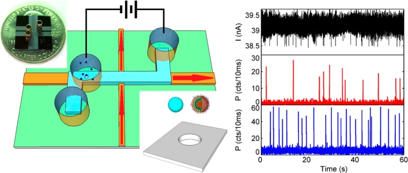
The analysis of individual biological nanoparticles has significantly advanced our understanding of fundamental biological processes but is also rapidly becoming relevant for molecular diagnostic applications in the emerging field of personalized medicine. Both optical and electrical methods for the detection and analysis of single biomolecules have been developed, but they are generally not used in concert and in suitably integrated form to allow for multimodal analysis with high throughput. Here we report on a dual-mode electrical and optical single-nanoparticle sensing device with capabilities that would not be available with each technique individually. The new method is based on an optofluidic chip with an integrated nanopore that serves as a smart gate to control the delivery of individual nanoparticles to an optical excitation region for ensemble-free optical analysis in rapid succession. We demonstrate electro-optofluidic size discrimination of fluorescent nanobeads, electro-optical detection of single fluorescently labeled influenza viruses, and the identification of single viruses within a mixture of equally sized fluorescent nanoparticles with up to 100% fidelity.
Keywords: Nanopores, optofluidics, single virus detection, correlated detection, lab-on-a-chip, fluorescence spectroscopy
Optofluidic integration has recently garnered a lot of attention.1−3 The combination of integrated optics with microfluidics on a single-chip-scale system promises novel instruments and devices based on dynamic reconfiguration4 as well as integration of both fluidic and optical functionalities toward a complete lab-on-a-chip.2 A number of approaches have been used to incorporate waveguide-based optical guiding with fluidic devices, including photonic crystal waveguides, slot waveguides, and optofluidic ring resonators.5−7 Liquid-core antiresonant reflecting optical waveguides (ARROWs) are the basis of a self-contained optofluidic platform in which solid-core and liquid-core waveguides can be interfaced in a planar fashion to deliver and collect light from the fluidic waveguide channel (see Figure 1a). In this approach, particles inside the channel experience the full intensity of the waveguide mode, and the orthogonal waveguide intersection creates small excitation volumes that result in single-particle optical detection sensitivity.8,9 However, this basic layout leaves some ambiguity regarding the exact number of particles causing individual fluorescence bursts. In addition, it does not allow for controlled delivery and analysis of a single particle to the excitation point, which is important for single-molecule analysis. A nanopore (i.e., a nanoscopic opening in a biological or solid-state membrane) can provide such a gating capability. Moreover, nanopores have become quite popular as single-molecule electrical sensors because each particle that moves through the opening under an applied field produces a characteristic current blockade signature.10 This electrical detection principle has been vigorously pursued for rapid and low-cost de novo sequencing as well as analysis of proteins and other small molecules.11−16 Recently, nanopore detection has been combined with microscope-based fluorescence imaging to visualize particle translocations and track particle movement around the nanopore.17−21 However, the availability of two independent particle-characteristic signals opens additional analytic capabilities, in particular for more complex solutions with multiple particle types. Moreover, full electro-optofluidic integration of fluidic, optical, and electrical control on a single chip has not been demonstrated.22
Figure 1.
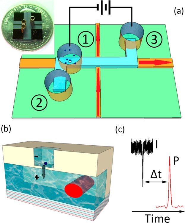
Nanopore-gated optofluidic device. (a) Schematic view of intersecting solid-core (orange) and liquid-core (blue) optical waveguides on a silicon chip with particles and electrodes in metal reservoirs. The inset shows a photograph of chip. (b) Schematic view of particle translocation through a nanopore milled into the bottom of a silicon dioxide layer; the red area shows the optical excitation volume defined by the fwhm area of the optical waveguide mode traversing the liquid core. (c) Principle of dual-mode electro-optical single-molecule detection, in which each particle produces two characteristic signals, a transient current decrease and a fluorescence spike, separated by a characteristic time Δt.
Here we present the first demonstration of multimodal electro-optical analysis of single nanoparticles on an optofluidic chip with optical sensitivity to individual fluorescently labeled nanoparticles and biomolecules. A solid-state nanopore23,24 is incorporated as a “smart gate” that not only ensures controlled delivery of individual particles for optical detection but also provides a characteristic electrical signal for further analysis. The integrated device can identify fluorescent nanoparticles according to their size, determine on-chip flow speed by cross-correlation of optical and electrical signals, unambiguously detect single fluorescently labeled influenza viruses, and identify single viruses within a mixture of equally sized fluorescent particles. Particle identification occurs in rapid succession with up to 100% fidelity, suggesting that an electro-optofluidic chip can form the basis of a high-throughput particle analysis platform.
Results.Setup and Operating Principle. Figure 1a shows a schematic view of the electro-optical sensing device. It is based on solid-core (orange) and liquid-core (blue) ARROWs that form an orthogonal intersection with an optical excitation/detection volume of ∼100 fL, enabling single-bioparticle fluorescence detection using planar optical integration.8,9 The device is constructed on a silicon wafer using standard micromachining techniques, and optical confinement is provided by alternating thin films of silicon dioxide and tantalum oxide. A nanopore is added to this device by a two-step focused ion beam milling process: first, a 2 μm × 2 μm microscale well is opened in the thick top oxide over the liquid-core ARROW; second, the nanopore is formed in the remaining SiO2 membrane of ∼170 nm thickness.
Details, including images of the waveguide structure, the optical modes, nanopore top and side views, and the electric field distribution in the micropore/nanopore construct can be found in the Supporting Information. Fluid reservoirs (∼6 μL volume) are attached over the ends of the liquid-core channel and over the nanopore, as shown in Figure 1. Solutions containing nanoparticles are introduced into reservoir 1, and individual particles are drawn through the nanopore into the waveguide channel by a voltage applied between reservoirs 1 and 3. Once inside the channel, particles can be moved toward the optical excitation spot either electrokinetically9 or by pressure applied between reservoirs 2 and 3. In the present study, particle movement along the liquid-core waveguide channel was created with hydrostatic pressure created by unequal filling of reservoirs 2 and 3. The Figure 1a inset shows a photograph of the entire ∼1 cm2 chip, and Figure 1c illustrates the operational principle of the dual-mode single-particle analysis device. Upon translocation through the nanopore into the ARROW channel, nanoparticles generate a particle-dependent, characteristic current blockade [a dip in the ionic current I(t)]. They then pass through the optical excitation spot and generate a second specific signal, a spike in the optical signal P(t) that is collected at the chip edge with a photodetector. Ideally, the two signals originate from single particles and should be highly correlated, providing both optical and electrical information. It should be noted that the optical beam path runs in the plane of the chip and that the waveguide mode is confined in the channel below the nanopore (Figure 1b). This means that particles can be excited only after they pass through the nanopore, even if the nanopore is placed directly above the optical excitation spot. This arrangement eliminates inadvertent photobleaching of fluorescent labels before the particle moves through the pore and ensures that the detection of an optical signal identifies a complete translocation event.
Electro-optical Analysis of a Nanobead Mixture. In order to demonstrate the ability of the nanopore device to act as a smart gate with optical and electrical single-particle resolution, we introduced a mixture of fluorescent nanoparticles with different diameters (100 and 200 nm) to a 250 nm pore (Figure 2a). All of the aqueous solutions were filtered with a 10 nm filter (Whatman Antop 10). The nanoparticles (TetraSpeck Microspheres 0.2 μm/0.1 μm, FluoSpheres Carboxylate-Modified Microspheres 0.1 μm) were suspended in 0.01 M potassium chloride solution (20 mM BICINE, pH 7.6, 0.01% v/v Triton X-100), and the final concentrations of 200 and 100 nm nanobeads were 7.48 × 10⁻¹² and 6.05 × 10⁻¹¹ M, respectively. An Axon Axopatch 200B patch-clamp amplifier was used to apply a voltage across the nanopore. After the analog signal was filtered by an on-board 10 kHz low-pass Bessel filter, it was digitized by an Axon Digidata 1440A digitizer at 250 kHz. A He–Ne laser (632.8 nm) and an argon laser (488 nm) were used as the excitation light sources. The optical signal was spectrally filtered and collected by two avalanche photodiodes. Before the voltage was applied across the nanopore, a synchronizing TTL signal generated by the digitizer was sent to a time-correlated single-photon counting board (Picoquant, TimeHarp 200) to trigger the optical recording. We verified that this method leads to very uniform pressure and velocities over the duration of an experiment. The electrical current I(t) (top) and optical fluorescence P(t) (bottom) were then recorded for an applied voltage of 3 V and are displayed in Figure 2b. Clear signals can be observed in both traces, and the signals are highly correlated in time. This correlation was verified by computing the cross-correlation C(τ) between I(t) and P(t) (Figure 2c). Because of the different shapes and durations of the electrical and optical signals, the raw optical and electrical signals were replaced with normalized pulses at the peak positions for cross-correlation calculations. C(τ) was then calculated using the normalized signals with the crosscorr function in MATLAB. The cross-correlation C(τ) between I(t) and P(t) exhibits a single, well-defined peak at τ = 5.8s. This corresponds to the time required for the particles to travel from the nanopore to the optical excitation spot under the applied pressure. Since all of the physical dimensions are known, we can immediately extract the velocity as 270 μm/s, in excellent agreement with the value expected from the temporal width of the optical pulses (Figure 2b inset) and the width of the waveguide mode. No spurious optical peaks without corresponding electrical current blockades were observed, confirming the absence of simultaneous translocations of multiple particles through the nanopore.
Figure 2.
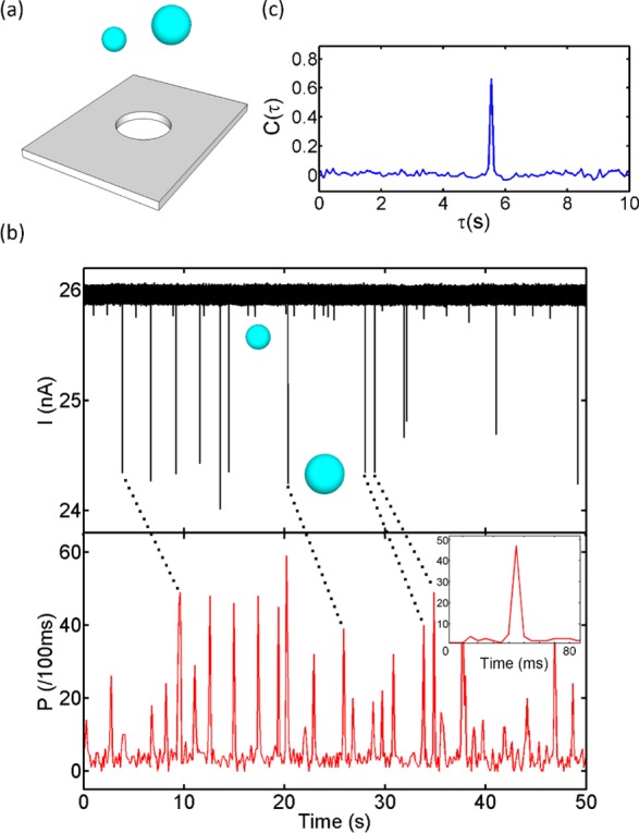
Gated electro-optical detection of single nanobeads. (a) Fluorescent nanobeads of two different diameters (100/200 nm) are translocated through a 250 nm nanopore. (b) Electrical blockade (top) and optical fluorescence (bottom) signals showing correlated single-particle detection events (four examples are highlighted with dashed lines). The inset shows a zoomed-in view of the optical signal with average width of 8 μs. (c) Cross-correlation of the electrical and optical signals, C(τ), which shows a single peak that enables accurate determination of the flow velocity in the waveguide channel. The particle translocation rate was 35.6 particles/min, but rates in excess of 1000 particles/s are possible.25
Figure 3a shows the distribution of the optically detected signal amplitudes. Ideally one would expect two subpopulations corresponding to the larger/brighter and smaller/darker nanobeads, respectively. However, this information is almost completely lost as a result of statistical variations in the particle brightness and the exact location within the optical excitation volume. The electrical signal depicted in Figure 3b, on the other hand, shows two well-separated subpopulations, allowing for identification of particle size by the depth of the current blockade. Because of their 1:1 correspondence, the optical and electrical signals can be combined as shown in Figure 3c, which plots the optical brightness versus the blockade amplitude for each detected particle. This clarifies the distribution of optical signals, and the optical properties can be analyzed for each particle size. While the larger particles are indeed generally brighter (Pave = 591 counts/s, σ = 18.9 counts/s) compared with the smaller ones (Pave = 238 counts/s, σ = 9.9 counts/s), there is a brightness region (indicated by the dashed lines) in which the particle subpopulations cannot be resolved using the optical signal alone. Because single nanoparticles can be detected both electrically and optically, the nanopore gate enables direct extraction of the flow speed as well as unambiguous particle discrimination and resolution of the optical fluorescence statistics.
Figure 3.
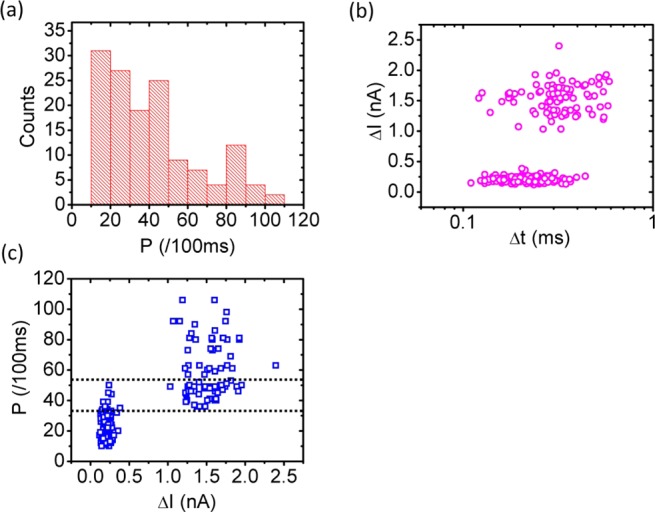
Identification of nanobead subpopulations. (a) Fluorescence intensity histogram. (b) Scatter plot of electrical blockades revealing the two subpopulations by current blockade depth. (c) Multiparameter analysis enabling assignment of optical properties to bead subpopulations. The dashed lines show the optical signal range with ambiguous particle size assignment.
Electro-optical Detection of Single Influenza Viruses. In order to demonstrate that dual-mode single-molecule analysis is applicable to biologically relevant nanoparticles, we fluorescently labeled influenza A H1N1 viruses (80–120 nm diameter) and introduced them to a d =157 nm pore (Figure 4a). Purified human influenza A/PR/8/34 (H1N1) was obtained from Advanced Biotechnologies. The viral concentration was specified at 5.3 × 10¹¹ virus particles/mL prior to inactivation. The viral capsids were labeled using monoreactive Cy5 dye (Amersham) according to the manufacturer instructions. The labeled virus was separated from unreacted dye using a PD midiTrapTM G-25 column (GE Healthcare). The first eluted fraction (flow through) was used for subsequent testing. Figure 4b shows a subset of the electrical and optical signals obtained at an applied voltage of 4 V. The apparent correlation between the signals is again obvious from the raw data traces. Figure 4c shows very uniform blockade depths and durations, suggesting that individual virus particles are detected during translocation. This was unambiguously confirmed by the cross-correlation (Figure 4d), which again shows a single peak without any measurable delay since the nanopore was placed directly on top of the optical excitation spot (see the Supporting Information). All of the viruses were detected with 100% fidelity (each current blockade had a corresponding optical peak and vice versa) as a result of the close proximity of the nanopore and the optical excitation region. While false readings due to incomplete labeling or particle adhesion on the wall can occur in principle, very high detection fidelity and correlation can be consistently expected. These results represent the first unambiguous optical detection of single virus particles on a chip and the simultaneous characterization of their electrical blockade properties.
Figure 4.
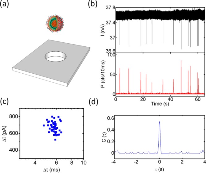
Electro-optical detection of single H1N1 influenza A viruses. (a) Schematic view of 120 nm virus particles and the 157 nm nanopore. (b) Electrical blockade (top) and optical fluorescence (bottom) signals showing correlated single-virus detection events. (c) Scatter plot of electrical signals showing narrowly distributed blockade depths and dwell times. (d) Cross-correlation of the optical and electrical virus detection signals.
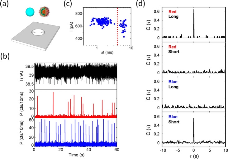
Electro-optical Identification of a Virus Subpopulation from a Nanoparticle Mixture. Finally, we introduced a mixture of almost equally sized nanobeads (100 nm, fluorescing at 515 nm) and labeled virus particles (80–120 nm, fluorescing at 670 nm) to the same nanopore (Figure 5a). Here the fluorescence was routed through a dichroic mirror and then spectrally filtered for the two colors used. The electrical signal trace in Figure 5b shows clear blockade events of the same magnitude as in Figure 4, albeit somewhat noisier, and a detection rate of 22.4 particles/min. The particles can be identified cleanly with the help of the optical signal, which is shown for both the red (virus) and blue (nanobead) channels. Again, a 1:1 correspondence with 100% detection fidelity is observed for a total of 144 nanoparticles.
Figure 5.
Identification of influenza viruses within a heterogeneous particle mixture. (a) Schematic view of the virus/nanobead mixture and nanopore. (b) Electrical blockade (top) and spectrally resolved optical fluorescence signals from viruses (center; red fluorescence) and nanobeads (bottom; blue). (c) Scatter plot of electrical signals suggesting nearly identical blockade depths but particle-dependent dwell times. (d) Cross-correlations of the optical and electrical virus detection signals for various combinations of dwell-time/spectral subpopulations, enabling unambiguous identification and assignment of viruses to long (>4 ms) dwell times.
The scatter plot for the electrical signal (Figure 5c) shows very uniform blockade depths, as would be expected given the almost identical particle sizes, and a relatively continuous distribution of the dwell times. However, the additional information provided by the spectral assignment of the optical signal allows for clear distinction of the electrical particle properties. When the electrical signal was separated into two dwell-time subpopulations (short and long) by the vertical dashed line and cross-correlated with the optical channels (red and blue), the four cross-correlation signals shown in Figure 5d were obtained. These immediately identify all of the particles, showing that viruses (red) have long dwell times (>4 ms) while the nanobeads (blue) have shorter dwell times (<4 ms) as a result of their different physical properties such as surface charge and mass. We note that this assignment is error-free, as is evident from the complete absence of correlations in the (red, short) and (blue, long) cases. These results show that we can both count and identify labeled pathogens unambiguously from a particle mixture using the combination of electrical and optical signal channels.
Discussion. Electro-optical analysis combining a smart nanopore gate and optical fluorescence detection on a planar optofluidic chip is a new approach for studying single nanoparticles that is more powerful than either method alone. For example, the 1:1 correspondence between the electrical and optical signals confirms the single-particle source of each signal and rules out spurious events such as transient blockades of the nanopore or optical noise. A variety of nanoparticles were identified using different combinations of optical and electrical parameters (fluorescence intensity, wavelength, current blockade depth, and dwell time). The results show that specific subpopulations can be identified within a complex, heterogeneous mixture. In particular, we were able to count and identify individual viruses both optically and electrically. This ability has a number of applications, such as direct counting of viruses and viral subpopulations; assessment of the degree of protein binding in an analyte as different sized clusters move through the nanopore and fluid channels at different rates; and the measurement of electrophoretic velocities of single molecules without any ensemble effects. Moreover, the device can easily be adapted to other optical methods such as Raman scattering or Rayleigh scattering. The method can also be extended to add a feedback mechanism that lowers the applied voltage upon detection of a blockade event. This would introduce one, and only one, nanoparticle into the channel for prolonged optical analysis. In combination with single-particle trapping methods,26,27 a powerful, high-throughput instrument for single-molecule analysis would be created. Finally, the implementation of both electrical and optical single-molecule analysis techniques on a single chip that can be easily integrated with microfluidic sample processing and delivery28 suggests that this approach can quickly find its way to both a large number of research laboratories and clinical applications.
Acknowledgments
We thank M. Rudenko for fruitful discussions and T. Yuzvinsky for assistance with ion beam milling and scanning electron microscopy imaging. We acknowledge support by the W. M. Keck Center for Nanoscale Optofluidics at UC Santa Cruz, the NSF (Grants ECS-0528714 and ECS-0528730), and the NIH (Grants R01EB006097 and R21EB008802).
Supporting Information Available
Chip fabrication and waveguide structure, nanopore drilling and characterization, optical excitation waveguide characterization, nanopore fabrication on the thick top SiO2 layer, implementation of delay-free correlated optoelectrical detection, top and side views of a 157 nm wide nanopore, and electric potential and electric field distributions around a nanopore. This material is available free of charge via the Internet at http://pubs.acs.org.
The authors declare no competing financial interest.
Funding Statement
National Institutes of Health, United States
Supplementary Material
References
- Fan X.; White I. M. Nat. Photonics 2011, 5, 591–597. [DOI] [PMC free article] [PubMed] [Google Scholar]
- Schmidt H.; Hawkins A. R. Nat. Photonics 2011, 5, 598–604. [Google Scholar]
- Erickson D.; Sinton D.; Psaltis D. Nat. Photonics 2011, 5, 583–590. [Google Scholar]
- Psaltis D.; Quake S. R.; Yang C. Nature 2006, 442, 381–386. [DOI] [PubMed] [Google Scholar]
- Mandal S.; Goddard J. M.; Erickson D. Lab Chip 2009, 9, 2924–2932. [DOI] [PubMed] [Google Scholar]
- Yang A. H. J.; Moore S. D.; Schmidt B. S.; Klug M.; Lipson M.; Erickson D. Nature 2009, 457, 71–75. [DOI] [PubMed] [Google Scholar]
- Fan X.; Yun S.-H. Nat. Methods 2014, 11, 141–147. [DOI] [PMC free article] [PubMed] [Google Scholar]
- Yin D.; Deamer D. W.; Schmidt H.; Barber J. P.; Hawkins A. R. Opt. Lett. 2006, 31, 2136–2138. [DOI] [PubMed] [Google Scholar]
- Yin D.; Lunt E. J.; Rudenko M. I.; Deamer D. W.; Hawkins A. R.; Schmidt H. Lab Chip 2007, 7, 1171–1175. [DOI] [PubMed] [Google Scholar]
- Kasianowicz J. J.; Brandin E.; Branton D.; Deamer D. W. Proc. Natl. Acad. Sci. U.S.A. 1996, 93, 13770–13773. [DOI] [PMC free article] [PubMed] [Google Scholar]
- Nakane J. J.; Akeson M.; Marziali A. J. Phys.: Condens. Matter 2003, 15, R1365–R1393. [Google Scholar]
- Clarke J.; Wu H.-C.; Jayasinghe L.; Patel A.; Reid S.; Bayley H. Nat. Nanotechnol. 2009, 4, 265–270. [DOI] [PubMed] [Google Scholar]
- Branton D.; Deamer D. W.; Marziali A.; Bayley H.; Benner S. A.; Butler T.; Di Ventra M.; Garaj S.; Hibbs A.; Huang X.; Jovanovich S. B.; Krstic P. S.; Lindsay S.; Ling X. S.; Mastrangelo C. H.; Meller A.; Oliver J. S.; Pershin Y. V.; Ramsey J. M.; Riehn R.; Soni G. V.; Tabard-Cossa V.; Wanunu M.; Wiggin M.; Schloss J. A. Nat. Biotechnol. 2008, 26, 1146–1153. [DOI] [PMC free article] [PubMed] [Google Scholar]
- Manrao E. A.; Derrington I. M.; Laszlo A. H.; Langford K. W.; Hopper M. K.; Gillgren N.; Pavlenok M.; Niederweis M.; Gundlach J. H. Nat. Biotechnol. 2012, 30, 349–353. [DOI] [PMC free article] [PubMed] [Google Scholar]
- Nivala J.; Marks D. B.; Akeson M. Nat. Biotechnol. 2013, 31, 247–250. [DOI] [PMC free article] [PubMed] [Google Scholar]
- Wei R.; Gatterdam V.; Wieneke R.; Tampé R.; Rant U. Nat. Nanotechnol. 2012, 7, 257–263. [DOI] [PubMed] [Google Scholar]
- Heron A. J.; Thompson J. R.; Cronin B.; Bayley H.; Wallace M. I. J. Am. Chem. Soc. 2009, 131, 1652–1653. [DOI] [PubMed] [Google Scholar]
- Keyser U. F.; Koeleman B. N.; van Dorp S.; Krapf D.; Smeets R. M. M.; Lemay S. G.; Dekker N. H.; Dekker C. Nat. Phys. 2006, 2, 473–477. [Google Scholar]
- Kurz V.; Nelson E. M.; Shim J.; Timp G. ACS Nano 2013, 7, 4057–4069. [DOI] [PubMed] [Google Scholar]
- Thacker V. V.; Ghosal S.; Hernández-Ainsa S.; Bell N. A. W.; Keyser U. F. Appl. Phys. Lett. 2012, 101, 223704. [DOI] [PMC free article] [PubMed] [Google Scholar]
- Soni G. V.; Singer A.; Yu Z.; Sun Y.; McNally B.; Meller A. Rev. Sci. Instrum. 2010, 81, 014301. [DOI] [PMC free article] [PubMed] [Google Scholar]
- Craighead H. Nature 2006, 442, 387–393. [DOI] [PubMed] [Google Scholar]
- Li J.; Stein D.; McMullan C.; Branton D.; Aziz M. J.; Golovchenko J. A. Nature 2001, 412, 166–169. [DOI] [PubMed] [Google Scholar]
- Dekker C. Nat. Nanotechnol. 2007, 2, 209–215. [DOI] [PubMed] [Google Scholar]
- Rudenko M. I.; Holmes M. R.; Ermolenko D. N.; Lunt E. J.; Gerhardt S.; Noller H. F.; Deamer D. W.; Hawkins A.; Schmidt H. Biosens. Bioelectron. 2011, 29, 34–39. [DOI] [PubMed] [Google Scholar]
- Cohen A. E.; Moerner W. E. Proc. Natl. Acad. Sci. U.S.A. 2006, 103, 4362–4365. [DOI] [PMC free article] [PubMed] [Google Scholar]
- Fields A. P.; Cohen A. E. Proc. Natl. Acad. Sci. U.S.A. 2011, 108, 8937–8942. [DOI] [PMC free article] [PubMed] [Google Scholar]
- Parks J. W.; Cai H.; Zempoaltecatl L.; Yuzvinsky T. D.; Leake K.; Hawkins A. R.; Schmidt H. Lab Chip 2013, 13, 4118–4123. [DOI] [PMC free article] [PubMed] [Google Scholar]
Associated Data
This section collects any data citations, data availability statements, or supplementary materials included in this article.


