Significance
Coherence of electronic states is crucial for quantum manipulation through light–matter interactions. To achieve coherence in conventional solid-state systems, extreme conditions such as cryogenic temperatures are required, which is a long-term challenge for practical applications. The emerging atomically thin transition metal dichalcogenides provide an unprecedented platform to explore the interplay of quantum states of spin and valley. In this paper, we demonstrate room-temperature valley coherence and valley polarization in bilayer WS2 with polarization-resolved photoluminescence measurements. The robustness of the valley coherence and valley polarization is understood as the consequence of the coupling of spin, layer, and valley degrees of freedom in bilayer WS2. It inspires new perspectives on quantum manipulations in 2D solid-state systems.
Keywords: valleytronics, spin–valley coupling, valley quantum control
Abstract
We report the observation of anomalously robust valley polarization and valley coherence in bilayer WS2. The polarization of the photoluminescence from bilayer WS2 follows that of the excitation source with both circular and linear polarization, and remains even at room temperature. The near-unity circular polarization of the luminescence reveals the coupling of spin, layer, and valley degree of freedom in bilayer system, and the linearly polarized photoluminescence manifests quantum coherence between the two inequivalent band extrema in momentum space, namely, the valley quantum coherence in atomically thin bilayer WS2. This observation provides insight into quantum manipulation in atomically thin semiconductors.
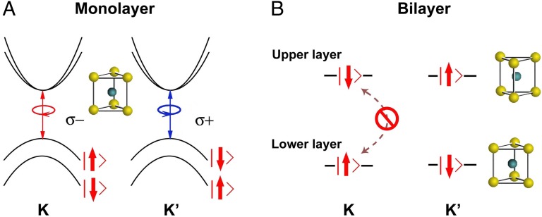
Tungsten sulfide WS2, part of the family of group VI transition metal dichalcogenides (TMDCs), is a layered compound with buckled hexagonal lattice. As WS2 thins to atomically thin layers, WS2 films undergo a transition from indirect gap in bulk form to direct gap at monolayer level with the band edge located at energy-degenerate valleys (K, K′) at the corners of the Brillouin zone (1–3). Like the case of its sister compound, monolayer MoS2, the valley degree of freedom of monolayer WS2 could be presumably addressed through nonzero but contrasting Berry curvatures and orbital magnetic moments that arise from the lack of spatial inversion symmetry at monolayers (3, 4). The valley polarization could be realized by the control of the polarization of optical field through valley-selective interband optical selection rules at K and K′ valleys as illustrated in Fig. 1A (4–6). In monolayer WS2, both the top of the valence bands and the bottom of the conduction bands are constructed primarily by the d orbits of tungsten atoms, which are remarkably shaped by spin–orbit coupling (SOC). The giant spin–orbit coupling splits the valence bands around the K (K′) valley by 0.4 eV, and the conduction band is nearly spin degenerated (7). As a result of time-reversal symmetry, the spin splitting has opposite signs at the K and K′ valleys. Namely, the Kramer’s doublet and is separated from the other doublet and by the SOC splitting of 0.4 eV. The spin and valley are strongly coupled at K (K′) valleys, and this coupling significantly suppresses spin and valley relaxations as both spin and valley indices have to be changed simultaneously.
Fig. 1.
(A) Schematic of valley-dependent optical selection rules and the Zeeman-like spin splitting in the valence bands of monolayer WS2. (B) Diagram of spin–layer–valley coupling in 2H stacked bilayer WS2. Interlayer hopping is suppressed in bilayer WS2 owing to the coupling of spin, valley, and layer degrees of freedom.
In addition to the spin and valley degrees of freedom, in bilayer WS2 there exists an extra index: layer polarization that indicates the carriers’ location, either up-layer or down-layer. Bilayer WS2 follows the Bernal packing order and the spatial inversion symmetry is recovered: each layer is 180° in plane rotation of the other with the tungsten atoms of a given layer sitting exactly on top of the S atoms of the other layer. The layer rotation symmetry switches K and K′ valleys, but leaves the spin unchanged, which results in a sign change for the spin–valley coupling from layer to layer (Fig. 1B). From the simple spatial symmetry point of view, one might expect that the valley-dependent physics fades at bilayers owing to inversion symmetry, as the precedent of bilayer MoS2 (8). Nevertheless, the inversion symmetry becomes subtle if the coupling of spin, valley, and layer indices is taken into account. Note that the spin–valley coupling strength in WS2 is around 0.4 eV (the counterpart in MoS2 ∼ 0.16 eV), which is significantly higher than the interlayer hopping energy (∼0.1 eV); the interlayer coupling at K and K′ valleys in WS2 is greatly suppressed as indicated in Fig. 1B (7, 9). Consequently, bilayer WS2 can be regarded as decoupled layers and it may inherit the valley physics demonstrated in monolayer TMDCs. In addition, the interplay of spin, valley, and layer degrees of freedom opens an unprecedented channel toward manipulations of quantum states.
Here we report a systemic study of the polarization-resolved photoluminescence (PL) experiments on bilayer WS2. The polarization of PL inherits that of excitations up to room temperature, no matter whether it is circularly or linearly polarized. The experiments demonstrate the valley polarization and valley coherence in bilayer WS2 as a result of the coupling of spin, valley, and layer degrees of freedom. Surprisingly, the valley polarization and valley coherence in bilayer WS2 are anomalously robust compared with monolayer WS2.
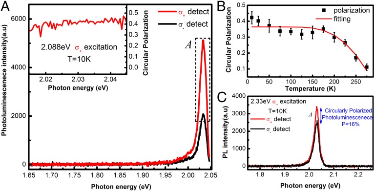
For comparison, we first perform polarization-resolved photoluminescence measurements on monolayer WS2. Fig. 2A shows the photoluminescence spectrum from monolayer WS2 at 10 K. The PL is dominated by the emission from band-edge excitons, so-called “A” exciton at K and K′ valleys. The excitons carry a clear circular dichroism under near-resonant excitation (2.088 eV) with circular polarization as a result of valley-selective optical selection rules, where the left-handed (right handed) polarization corresponds to the interband optical transition at K (K′) valley. The PL follows the helicity of the circularly polarized excitation optical field. To characterize the polarization of the luminescence spectra, we define a degree of circular polarization as , where I(σ±) is the intensity of the right- (left-) handed circular-polarization component. The luminescence spectra display a contrasting polarization for excitation with opposite helicities: P = 0.4 under σ+ excitation and P = −0.4 under σ− excitation on the most representative monolayer. For simplicity, only the PL under σ+ excitation is shown. The degree of circular polarization P is insensitive to PL energy throughout the whole luminescence as shown in Fig. 2A, Inset. These behaviors are fully expected in the mechanism of valley-selective optical selection rules (3, 4). The degree of circular polarization decays with increasing temperature and drops to 10% at room temperature (Fig. 2B). It decreases as the excitation energy shifts from the near-resonance energy of 2.088 to 2.331 eV as illustrated in Fig. 2C. The peak position of A exciton emission at band edges shifts from 2.04 eV at 10 K to 1.98 eV at room temperature. The energy difference between the PL peak and the near-resonance excitation (2.088 eV) is around 100 meV at room temperature, which is much smaller than the value 290 meV for the low temperature off-resonance excitation at 2.331 eV. However, the observed polarization for off-resonance excitation at 10 K (P = 16%) is much higher than the near-resonance condition at room temperature (P = 10%). It clearly shows that the depolarization cannot be attributed to single process, namely the off-resonance excitation or band-edge phonon scattering only (10).
Fig. 2.
Photoluminescence of monolayer WS2 under circularly polarized excitation. (A) Polarization resolved luminescence spectra with σ+ detection (red) and σ− detection (black) under near-resonant σ+ excitation (2.088 eV) at 10 K. Peak A is the excitonic transition at band edges of K (K′) valleys. Opposite helicity of PL is observed under σ− excitation. Inset presents the degree of the circular polarization at the prominent PL peak. (B) The degree of the circular polarization as a function of temperature. The curve (red) is a fit following a Boltzmann distribution where the intervalley scattering by phonons is assumed. (C) Photoluminescence spectrum under off-resonant σ+ excitation (2.33 eV) at 10 K. The red (black) curve denotes the PL circular components of σ+ (σ−).
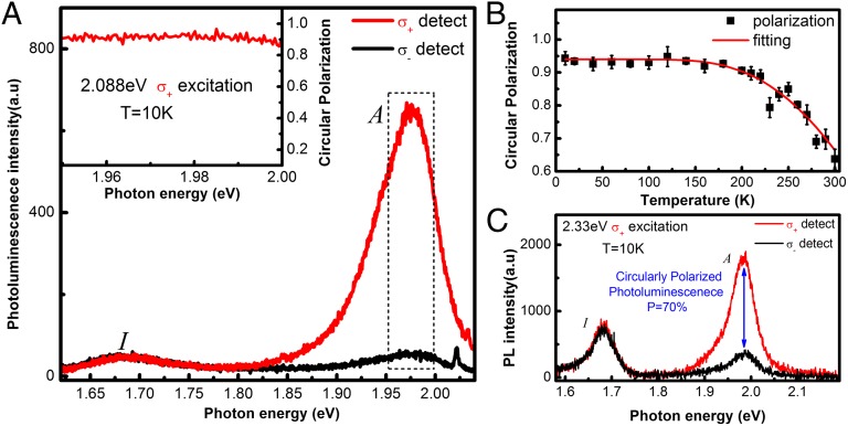
Next we study the PL from bilayer WS2. Fig. 3 shows the PL spectrum from bilayer WS2. The peak labeled as “I” denotes the interband optical transition from the indirect band gap, and the peak A corresponds to the exciton emission from direct band transition at K and K′ valleys. Although bilayer WS2 has an indirect gap, the direct interband optical transition at K and K′ valleys dominates the integrated PL intensity as the prerequisite of phonon/defect scattering is waived for direct band emission and the direct gap is just slightly larger than the indirect band gap in bilayers. Fig. 3A displays surprisingly robust PL circular dichroism of A exciton emission under circularly polarized excitations of 2.088 eV (resonance) and 2.331 eV (off resonance). The degree of circular polarization of A exciton emission under near-resonant σ± excitation is near unity (around 95%) at 10 K and preserves around 60% at room temperature. In contrast, the emission originating from indirect band gap is unpolarized in all experimental conditions.
Fig. 3.
Photoluminescence of bilayer WS2 under circularly polarized excitations. (A) Polarization-resolved luminescence spectra with components of σ+ (red) and σ− (black) under near-resonant σ+ excitation (2.088 eV) at 10 K. Peak A is recognized as the excitonic transition at band edge of direct gap. Peak I originates from the indirect band-gap emission, showing no polarization. Inset presents the circular polarization of the A excitonic transition around the PL peak. Opposite helicity of PL is observed under σ− excitation. (B) The degree of circular polarization as a function of temperature (black). The curve (red) is a fit following a Boltzman distribution where the intervalley scattering by phonons is assumed. (C) Photoluminescence spectrum of components of σ+ (red) and σ− (black) under off-resonance σ+ excitation (2.33 eV) at 10 K. A nonzero circular polarization P is only observed at emissions from A excitons.
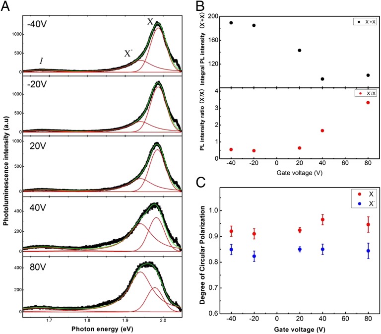
To exclude the potential cause of charge trapping or substrate charging effect, we study the polarization-resolved PL of bilayer WS2 with an out-plane electric field. Fig. 4A shows the evolution of PL spectra in a field-effect-transistor-like device under circularly polarized excitations of 2.088 eV and an electric gate at 10 K. The PL spectra dominated by A exciton show negligible change under the gate bias in the range of −40 to 20 V. The electric-conductance measurements show that the bilayer WS2 stays at the electrically intrinsic state under the above bias range. The PL spectra can be safely recognized as emissions from free excitons. As the gate bias switches further to the positive side (>20 V), the PL intensity decreases, and the emission from electron-bounded exciton “X−,” the so-called trion emerges and gradually raises its weight in the PL spectrum (11, 12). The electron–exciton binding energy is found to be 45 meV. Given only one trion peak in PL spectra, the interlayer trion (formed by exciton and electron/hole in different layers) and intralayer trion (exciton and electron/hole in the same layer) could not be distinguished due to the broad spectral width (13). Both the free exciton and trion show slight red shifts with negative bias, presumably as a result of quantum-confined stark effect (14). At all of the bias conditions, the degree of circular polarization of the free exciton and trion stays unchanged within the experiment sensitivity as shown in Fig. 4C.
Fig. 4.
Electric-doping-dependent photoluminescence spectrum of bilayer WS2 field-effect transistor. (A) Luminescence spectra of bilayer WS2 at different gate voltage under near-resonant σ+ excitation (2.088 eV) at 10 K. X and X− denote neutral exciton and trion, respectively. Green curve is a fitting consisting of two Lorentzian peak fits (peak I and X−) and one Gaussian peak fit (peak X). (B) Intensity of exciton and trion emissions versus gate. (Upper) The gate-dependent integral PL intensity consisting of exciton (X) and trion (X−). (Lower) The ratio of the integral PL intensity of exciton versus that of trion, as a function of the gate voltage. (C) Degree of circular polarization of exciton (X, red) and trion (X−, blue) versus the gate.
It is also unlikely that the high polarization in bilayers results from the isolation of the top layer from the environments, as similar behaviors are observed in monolayer and bilayer WS2 embedded in polymethyl methaccrylate (PMMA) matrix or capped with a 20-nm-thick SiO2 deposition. The insensitivity of the circular-polarization degree on bias and environments rules out the possibility that the effects of Coulomb screening, charge traps, or charge transfers with substrates are the major causes for the robust circular dichroism in bilayers against monolayers.
One potential cause may result from the shorter lifetime of excitons at K (K′) valley for bilayer system. The band gap shifts from K and K′ points of the Brillouin zone in monolayers to the indirect gap between the top of the valence band at Γ points and the bottom of the conduction band in the middle of K and Γ points in bilayers. Combining our time-resolved pump-probe reflectance experiments (Supporting Information) and the observed relative PL strength between monolayer and bilayer (10:1), we infer the exciton lifetime at K (K′) valleys around 10 ps, a fraction of that at monolayers. If we assume (i) the PL circular polarization , where P0 is the theoretical limit of PL polarization, and τk and τ denote the valley lifetime and exciton lifetime respectively; and (ii) the valley lifetime is the same for both monolayers and bilayers, the shorter exciton lifetime will lead to significantly higher PL polarization. However, the difference in exciton lifetime between bilayers and monolayers is not overwhelming enough to be the major cause of robust polarization observed in the time-integrated PL in bilayers.
In monolayer WS2 under circularly polarized resonant excitations, the depolarization mainly comes from the intervalley scattering. In bilayers, the depolarization could be either via intervalley scattering within the layer in a similar way as in monolayers, or via interlayer hopping, which also requires spin flip. As we discussed above, the interlayer hopping at K valley is suppressed in WS2 as a result of strong SOC in WS2 and spin–layer–valley coupling, which were experimentally proved by the circular dichroism in PL from bilayers. The robust polarization in bilayers implies that the intervalley scattering within a layer is diminished compared with that in monolayers. There are two prerequisites for intervalley scattering within layers: conservation of crystal momentum and spin flip of holes. The crystal momentum conservation could be satisfied with the involvement of phonons at K points in the Brillouin zone or atomic size defects, presumably sharing the similar strength in monolayers and bilayers. Spin-flip process could be realized by three different spin scattering mechanisms, namely D’yakonov–Perel (DP) mechanism (15), Elliot–Yaffet (EY) mechanism (16), and Bir–Aronov–Pikus (BAP) mechanism (17, 18). The DP mechanism acts through a Lamor precession driven by electron wavevector k dependent spin–orbit coupling. It is thought to be negligible for spin flip along out-plane direction as the mirror symmetry with respect to the plane of W atoms secures a zero out-plane crystal electric field. Another possible driving force behind the DP mechanism could be the asymmetry owing to the interface with the substrate. This can be excluded by the similar behaviors, where the monolayers and bilayers WS2 are embedded in PMMA matrix or capped with a thin layer of SiO2. The negligible effect of electric gating on polarization also implies that the DP mechanism is weak in monolayer and bilayer WS2; the EY mechanism originates from scattering with phonons and defects. Its strength in bilayers and monolayers is likely to be at similar scale, and bilayers even have more low-frequency collective vibrational modes (19). Therefore, EY mechanism is unlikely to be the cause here; the BAP mechanism originates from the electron–hole exchange interaction. In monolayer and bilayer TMDCs, the optical features are dominated by the Wannier type, yet giant excitonic effect, and the exciton-binding energy in such intrinsic 2D semiconductors is estimated to be 0.6 ∼ 1 eV (20, 21). This giant exciton-binding energy indicates a mixture of electron and hole wavefunctions and, consequently, strong exchange interaction, which may contribute to the spin flip and intervalley scattering (5, 22). As the conduction band has a band mixing at K points, the spin flip of the electron would be a quick process. An analogous scenario is that the spin of holes relaxes in hundreds of femtoseconds or fewer in GaAs as a result of band mixing and spin–orbit coupling. The electron spin flip could lead to hole spin flip via strong exchange interaction accompanying intervalley scattering, which is realized by the virtual annihilation of a bright exciton in the K valley and then generation in the K′ valley or vice versa (22). This non-single-particle spin relaxation leads to valley depolarization instead of the decrease of luminescence intensity that results from coupling with dark excitons. Generally, the exciton-binding energy decreases with the relaxation of spatial confinement. However, first principle calculation shows that monolayer and bilayer WS2 share the similar band dispersion and effective masses around K valley in their Brillouin zone as a result of spin–valley coupling (7). It implies that the binding energy of excitons around K valley in bilayer WS2 is similar to or slightly less than that in monolayer WS2. As the exchange interaction is roughly proportional to the square of exciton binding energy, the spin-flip rate and consequently intervalley scattering via exciton exchange interactions is presumably comparable or smaller to some extent in bilayer WS2 (Supporting Information). Nevertheless, this is unlikely the major cause of the anomalously robust valley polarization in bilayer WS2.
Another possibility includes extra spin-conserving channels via intermediate intervalley-interlayer scatterings in bilayer WS2, which are absent in monolayers (23). The extra spin-conserving channel may compete with the spin-flip process and reduce the relative weight of spin-flip intervalley scattering to some extent. However, the mechanism and the strength are unclear so far. Overall, the robust circular polarization in bilayers likely results from combined effects of the shorter exciton lifetime, smaller exciton-binding energy, extra spin-conserving channels, and the coupling of spin, layer, and valley degrees of freedom, indicating the relatively weak intervalley scattering in bilayer system. Further quantitative study is necessary to elaborate the mechanism.
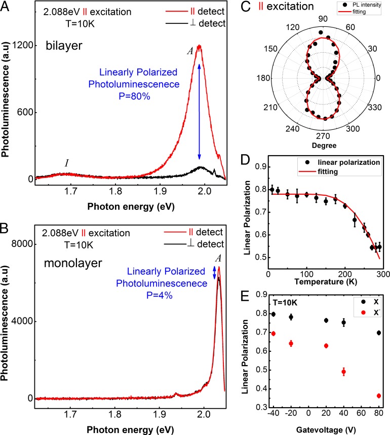
We also investigated the PL from bilayer WS2 under a linearly polarized excitation. A linearly polarized light could be treated as a coherent superposition of two opposite-helicity circularly polarized lights with a certain phase difference. The phase difference determines the polarization direction. In semiconductors, a photon excites an electron–hole pair with the transfer of energy, momentum, and phase information. The hot carriers energetically relax to the band edge in a quick process around 10−1 ∼ 101 ps through runs of inelastic and elastic scatterings, e.g., by acoustic phonons. During the quick relaxation process, generally the phase information randomizes and herein coherence fades. In monolayer TMDCs, the main channel for carrier relaxation is through intravalley scatterings including Coulomb interactions with electron (hole) and inelastic interactions with phonons, which are valley independent and preserve the relative phase between K and K′ valleys (24). In bilayer WS2, the suppression of intervalley scattering consequently leads to the suppression of inhomogeneous broadening in carrier’s phase term. Subsequently, the valley coherence demonstrated in monolayer WSe2 (24) is expected to be enhanced in bilayers (13). The valley coherence in monolayer and bilayer WS2 could be monitored by the polarization of PL under linearly polarized excitations.
Fig. 5A shows the linearly polarized components of PL under a linearly polarized excitation of 2.088 eV at 10 K. The emission from indirect band gap is unpolarized and A exciton displays a pronounced linear polarization following the excitation. The degree of linear polarization is around 80%, where I(∥)(I(⊥)) is the intensity of PL with parallel (perpendicular) polarization with respect to the excitation polarization. In contrast, the linear polarization is much weaker in monolayer samples (4% under the same experimental conditions, as shown in Fig. 5B). As presented in Fig. 5C, the polarization of A exciton is independent of crystal orientation and exactly follows the polarization of excitations. The degree of the linear polarization in bilayer WS2 slightly decreases with the increased temperature and drops from 80% at 10 K to 50% at room temperature (Fig. 5D). This is the paradigm of the robust valley coherency in bilayer WS2.
Fig. 5.
Linearly polarized excitations on monolayer and bilayer WS2. (A) Linear-polarization-resolved luminescence spectra of bilayer WS2 under near-resonant linearly polarized excitation (2.088 eV) at 10 K. Red (black) presents the spectrum with parallel (cross) polarization with respect to the linear polarization of excitation source. A linear polarization of 80% is observed for exciton A, and the indirect gap transition (I) is unpolarized. (B) Linear-polarization-resolved luminescence spectra of monolayer WS2 under near-resonant linearly polarized excitation (2.088 eV) at 10 K. Red (black) denotes the spectrum with the parallel (cross) polarization with respect to the linear polarization of excitation source. The linear polarization for exciton A in monolayer WS2 is much weaker, with a maximum value of 4%. (C) Polar plot for intensity of the exciton A in bilayer WS2 (black) as a function of the detection angle at 10 K. Red curve is a fit-following cos2(θ). (D) The degree of linear polarization of exciton A in bilayer WS2 (black) as a function of temperature. The curve (red) is a fit following a Boltzmann distribution where the intervalley scattering by phonons is assumed. (E) Electric doping dependence of the linear polarization of exciton A in bilayer WS2 at 10 K.
The linear polarization of both exciton and trion in bilayer, contrasting to the circular polarization, which is insensitive to the electric field in the range, shows a weak electric gating dependence as shown in Fig. 5E. The PL linear polarization, presenting valley coherence, decreases as the Fermi level shifts to the conduction band. It does not directly affect intervalley scattering within individual layers and makes negligible change in circular dichroism. Nevertheless, the electric field between the layers induces a layer polarization and slightly shifts the band alignments between the layers by different amounts in conduction and valence bands (13, 25), although the shift is indistinguishable in the present PL spectra due to the broad spectral width. The layer polarization and the shift of band alignments may induce a relative phase difference between two layers and therefore affect the PL linear polarization via interference. Further study is needed to fully understand the mechanism.
In summary, we demonstrated anomalously robust valley polarization and valley polarization coherence in bilayer WS2. The valley polarization and valley coherence in bilayer WS2 are the direct consequences of giant spin–orbit coupling and spin valley coupling in WS2. The depolarization and decoherence processes are greatly suppressed in bilayer, although the mechanism is ambiguous. The robust valley polarization and valley coherence make bilayer WS2 an intriguing platform for spin and valley physics.
Methods
Atomically thin WS2 films were fabricated by mechanical exfoliation from a synthetic single crystal, and the sample thickness was identified with optical microscope, photoluminescence spectroscopy, and second harmonic generation (7). The inversion symmetry of bilayer WS2 was confirmed by second harmonic generation experiments (7, 26, 27). All samples were mounted on heavily doped silicon substrates capped with 300-nm-thick oxide. Polarization-sensitive photoluminescence experiments was carried out with a confocallike setup, and the details can be found in ref. 6. The carrier dynamics measurement was carried out using the time-resolved pump-probe technique and the details can be found in the Supporting Information.
Supplementary Material
Acknowledgments
The authors thank Prof. Wang Yao and Prof. Ming-Wei Wu for helpful discussion. H.Z. acknowledges the support of Direct Grant for Research 2013/14 (P/4053082) in Chinese University of Hong Kong. J.D. acknowledges support from National Natural Science Foundation of China (11204184). The work is supported by Area of Excellency (AoE/P-04/08), University of Hong Kong (HKU) Strategic Research Themes (SRT) on New Materials, and Collaborative Research Fund of Hong Kong Research Grant Council (HKU9/CRF/13G).
Footnotes
The authors declare no conflict of interest.
This article is a PNAS Direct Submission.
This article contains supporting information online at www.pnas.org/lookup/suppl/doi:10.1073/pnas.1406960111/-/DCSupplemental.
References
- 1.Mak KF, Lee C, Hone J, Shan J, Heinz TF. Atomically thin MoS₂: A new direct-gap semiconductor. Phys Rev Lett. 2010;105(13):136805. doi: 10.1103/PhysRevLett.105.136805. [DOI] [PubMed] [Google Scholar]
- 2.Splendiani A, et al. Emerging photoluminescence in monolayer MoS2. Nano Lett. 2010;10(4):1271–1275. doi: 10.1021/nl903868w. [DOI] [PubMed] [Google Scholar]
- 3.Xiao D, Liu G-B, Feng W, Xu X, Yao W. Coupled spin and valley physics in monolayers of MoS2 and other group-VI dichalcogenides. Phys Rev Lett. 2012;108(19):196802. doi: 10.1103/PhysRevLett.108.196802. [DOI] [PubMed] [Google Scholar]
- 4.Cao T, et al. Valley-selective circular dichroism of monolayer molybdenum disulphide. Nat Commun. 2012;3:887. doi: 10.1038/ncomms1882. [DOI] [PMC free article] [PubMed] [Google Scholar]
- 5.Mak KF, He K, Shan J, Heinz TF. Control of valley polarization in monolayer MoS2 by optical helicity. Nat Nanotechnol. 2012;7(8):494–498. doi: 10.1038/nnano.2012.96. [DOI] [PubMed] [Google Scholar]
- 6.Zeng H, Dai J, Yao W, Xiao D, Cui X. Valley polarization in MoS2 monolayers by optical pumping. Nat Nanotechnol. 2012;7(8):490–493. doi: 10.1038/nnano.2012.95. [DOI] [PubMed] [Google Scholar]
- 7.Zeng H, et al. Optical signature of symmetry variations and spin-valley coupling in atomically thin tungsten dichalcogenides. Sci Rep. 2013;3:1608. doi: 10.1038/srep01608. [DOI] [PMC free article] [PubMed] [Google Scholar]
- 8.Wu S, et al. Electrical tuning of valley magnetic moment through symmetry control in bilayer MoS2. Nat Phys. 2013;9(3):149–153. [Google Scholar]
- 9.Gong Z, et al. Magnetoelectric effects and valley-controlled spin quantum gates in transition metal dichalcogenide bilayers. Nat Commun. 2013;4:2053. doi: 10.1038/ncomms3053. [DOI] [PubMed] [Google Scholar]
- 10.Kioseoglou G, et al. Valley polarization and intervalley scattering in monolayer MoS2. Appl Phys Lett. 2012;101(22):221907. [Google Scholar]
- 11.Ross JS, et al. Electrical control of neutral and charged excitons in a monolayer semiconductor. Nat Commun. 2013;4:1474. doi: 10.1038/ncomms2498. [DOI] [PubMed] [Google Scholar]
- 12.Mak KF, et al. Tightly bound trions in monolayer MoS2. Nat Mater. 2013;12(3):207–211. doi: 10.1038/nmat3505. [DOI] [PubMed] [Google Scholar]
- 13.Jones AM, et al. Spin-layer locking effects in optical orientation of exciton spin in bilayer WSe2. Nat Phys. 2014;10(2):130–134. [Google Scholar]
- 14.Miller DAB, et al. Band-edge electroabsorption in quantum well structures: The quantum-confined stark effect. Phys Rev Lett. 1984;53(22):2173–2176. [Google Scholar]
- 15.Dyakonov MI, Perel VI. Spin orientation of electrons associated with interband absorption of light in semiconductors. J Exp Theor Phys. 1971;33:1053. [Google Scholar]
- 16.Yafet Y. Calculation of the g factor of metallic sodium. Phys Rev. 1952;85(3):478–478. [Google Scholar]
- 17.Bir GL, Aronov AG, Pikus GE. Spin relaxation of electrons due to scattering by holes. J Exp Theor Phys. 1975;42:705–712. [Google Scholar]
- 18.Maialle MZ, Sham LJ, de Andrada e Silva EA. Exciton spin dynamics in quantum wells. Phys Rev B Condens Matter. 1993;47(23):15776–15788. doi: 10.1103/physrevb.47.15776. [DOI] [PubMed] [Google Scholar]
- 19.Zeng H, et al. Low-frequency Raman modes and electronic excitations in atomically thin MoS2 films. Phys Rev B. 2012;86(24):241301. [Google Scholar]
- 20.Cheiwchanchamnangij T, Lambrecht WRL. Quasiparticle band structure calculation of monolayer, bilayer, and bulk MoS2. Phys Rev B. 2012;85(20):205302. [Google Scholar]
- 21.Shi H, Pan H, Zhang Y-W, Yakobson BI. Quasiparticle band structures and optical properties of strained monolayer MoS2 and WS2. Phys Rev B. 2013;87(15):155304. [Google Scholar]
- 22.Yu T, Wu MW. Valley depolarization due to intervalley and intravalley electron-hole exchange interactions in monolayer MoS2. Phys Rev B. 2014;89(20):205303. [Google Scholar]
- 23.Song Y, Dery H. Transport theory of monolayer transition-metal dichalcogenides through symmetry. Phys Rev Lett. 2013;111(2):026601. doi: 10.1103/PhysRevLett.111.026601. [DOI] [PubMed] [Google Scholar]
- 24.Jones AM, et al. Optical generation of excitonic valley coherence in monolayer WSe2. Nat Nanotechnol. 2013;8(9):634–638. doi: 10.1038/nnano.2013.151. [DOI] [PubMed] [Google Scholar]
- 25.Yuan H, et al. Zeeman-type spin splitting controlled by an electric field. Nat Phys. 2013;9(9):563–569. [Google Scholar]
- 26.Kumar N, et al. Second harmonic microscopy of monolayer MoS2. Phys Rev B. 2013;87(16):161403. [Google Scholar]
- 27.Li Y, et al. Probing symmetry properties of few-layer MoS2 and h-BN by optical second-harmonic generation. Nano Lett. 2013;13(7):3329–3333. doi: 10.1021/nl401561r. [DOI] [PubMed] [Google Scholar]
Associated Data
This section collects any data citations, data availability statements, or supplementary materials included in this article.


