Abstract
Ring resonator modulators (RRM) combine extreme compactness, low power consumption and wavelength division multiplexing functionality, making them a frontrunner for addressing the scalability requirements of short distance optical links. To extend data rates beyond the classically assumed bandwidth capability, we derive and experimentally verify closed form equations of the electro-optic response and asymmetric side band generation resulting from inherent transient time dynamics and leverage these to significantly improve device performance. An equivalent circuit description with a commonly used peaking amplifier model allows straightforward assessment of the effect on existing communication system architectures. A small signal analytical expression of peaking in the electro-optic response of RRMs is derived and used to extend the electro-optic bandwidth of the device above 40 GHz as well as to open eye diagrams penalized by intersymbol interference at 32, 40 and 44 Gbps. Predicted peaking and asymmetric side band generation are in excellent agreement with experiments.
To support fast growing port counts of short distance optical links in data- and high-performance computing centers, integrated electro-optic (E/O) modulators and transceiver subsystems need to be low power and compact in addition to supporting high data rates. RRMs1 and their implementation in silicon technology2 combine extreme compactness and low power consumption3 with very high modulation speeds4,5,6 and may thus become an important building block in future interconnect systems. As mass-manufacturable optical interconnect technologies mature and become more affordable, their field of application penetrates to ever smaller architecture levels. After servicing ultra-high-speed links over distances down to a few meters, optical technologies may be applied to even smaller architectural levels within individual servers and supercomputers. Novel architectures such as optically enabled silicon interposers7 may enable ultra-high-speed intra-server chip-to-chip connectivity and support emerging applications such as RAM databases or massively parallelized solid-state memories driven by Big Data applications. Silicon Photonics has developed into an integrated E/O technology platform that can address these needs8.
Following the initial demonstration of silicon based RRMs with phase shifters based on forward biased PIN junctions2 and improvement of demonstrated data rates with pre-emphasis9, implementation with reverse biased P(I)N phase shifters has allowed reaching very high modulation speeds. With dimensions on the order of 10 μm, RRMs are not only extremely compact relative to non-resonant devices such as travelling wave Mach-Zehnder modulators10,11, but also combine modulation with frequency selectivity, thus allowing the realization of wavelength domain multiplexed (WDM) transmitters by cascading multiple RRMs on a single waveguide bus12 without requiring additional WDM multiplexers. Suitable compact light sources generating a complete comb of optical carriers with sufficiently narrow linewidth and low relative intensity noise have been realized, e.g., in the form of single section semiconductor comb lasers13,14 in which the spectrum of a Fabry-Perot laser is stabilized by means of mode-locking, or in the form of on-chip frequency conversion in monolithically integrated optical parametric oscillators15,16,17. Both classes of light sources have proven to be compatible with multi-channel high-speed communication, the latter supporting even demanding data formats such as complex coherent encoding18. Since their first demonstration in silicon technology2, RRMs have also been used for phase encoding19 or as phase shifters embedded in linear modulators20,21. Implementations with novel phase shifters such as silicon-organic hybrid slot waveguides22 as well as device implementation in a bulk CMOS compatible process flow23 have proven them to be versatile and widely applicable devices.
Due to their small dimensions, the capacitance (C) of RRMs is small compared to longer linear devices. Since the energy per bit associated with switching a lumped element load24 with a drive voltage V is given by CV2/4, this directly results in a much reduced RF power consumption, down to a few fJ/bit demonstrated so far25. While RRMs are also resonant devices with a narrow passband that need to be actively temperature stabilized, recent progress has been made in reducing the associated power consumption either by reducing the thermal sensitivity of the devices, e.g., by means of optical materials with opposing thermooptic coefficients26, or by increasing the power efficiency of the temperature tuning, e.g., by undercutting the structures27. With less than 100 fJ/bit added to the RF power consumption at 25 Gb/s in ref. 27, the energy efficiency of RRMs approaches that of much more exotic and challenging to integrate devices such as hybrid plasmonic-polymer phase modulators28.
The RF power enhancement can be predicted by a simple metric, the finesse F of the cavity given by the ratio of the free spectral range (the spectral distance between adjacent resonances) with the linewidth of the cavity. A reduced linewidth, and thus a higher quality factor (Q-factor), reduce the refractive index modulation required to achieve a given optical signal level. A smaller cavity, and thus a larger free spectral range, reduce the capacitance that has to be driven by the voltage source. It can be simply derived that a critically coupled RRM with a finesse F has 1.3F/π the power efficiency of a short lumped element modulator. Thus, while the latter can reach essentially the same small signal response (within a factor 2, see supplementary information), a RRM can be much more power efficient. Very small RRMs have been realized, with recent results reaching cavities as small as a few microns across25,29. The Q-factor on the other hand is typically limited by the required bandwidth of the device, so that electro-optic modulation efficiency and modulation bandwidth can be traded off against each other by statically or dynamically adjusting the Q-factor30,31.
Novel RRM configurations, for example with travelling wave electrodes32 or with modulation of the coupling strength to the bus waveguide33 have been proposed in order to increase the allowable Q-factor at high data rates. So far, however, lumped-element RRMs with resonant wavelength modulation (fig. 1) have found the widest reaching applicability. In these devices, the maximum Q-factor, and thus the resonant enhancement factor, are limited by the required E/O bandwidth. Simplified models assume it to be independently limited by two factors: The RC time constant of the phase shifter, resulting in one first order filter, and the lifetime τa of photons in the cavity, resulting in a second first order filter with a bandwidth 1/2πτa. The latter limits the maximum Q-factor that can be implemented, and thus ultimately the highest resonant enhancement that can be reached. Peaking in the transient modulator response arising from more complex time dynamics in the optical domain has been observed in several experimental studies6,9,12,34,35 with models of varying levels of complexity reported in the literature36,37,38. Here, we show that this transient response can be used to extend the frequency range of operation of RRMs beyond the cutoff predicted by the photon lifetime, extending the range of operation to higher data rates or, conversely, increasing the allowable Q-factor and reducing the RF power consumption. While this bandwidth improvement also comes at the cost of a reduced DC modulation efficiency, it provides an alternate and simpler path to reconfiguring optical transmitters. Moreover, a moderate improvement of the overall device performance can be achieved35.
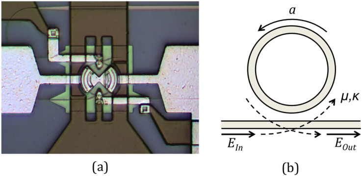
Figure 1. Micrograph of the fabricated device.
(a) Actual device, (b) Illustration of the symbols referred to in the text.
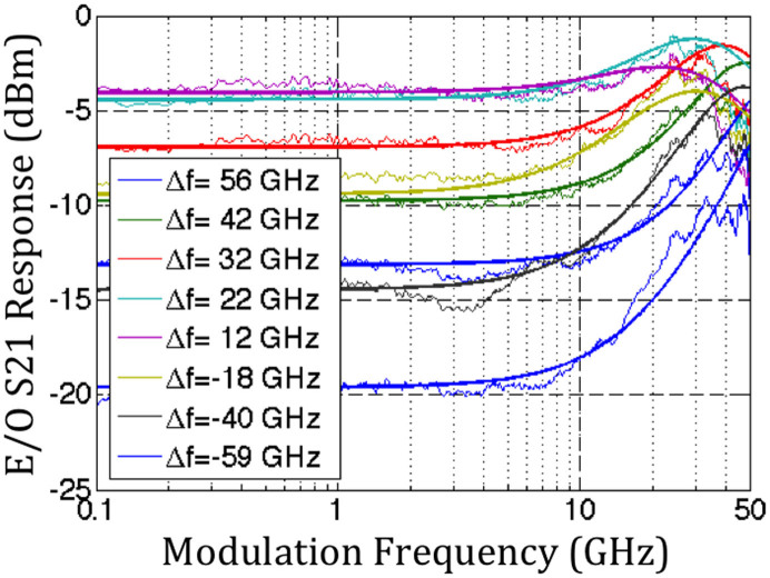
We apply a first order perturbation theoretical treatment to the differential equations used to describe the time dynamics in36,38 and derive a closed form expression of the frequency dependent small signal response of the modulator (E/O S-parameter) that matches very closely our measurements (fig. 2). Predicted asymmetric sideband generation is also verified experimentally (fig. 3), further confirming the model. After a theoretical investigation of peaking based enhancement (fig. 4), experimental characterization of optical links incorporating the RRM at 32, 40 and 44 Gbps demonstrates the capability of RRM peaking enhancement to enable high-speed optical links and to compensate for intersymbol interference (ISI) occurring elsewhere in the link (fig. 5). In order to make it straightforward for system architects not familiar with the intricacies of RRMs to leverage the peaking in communication systems, we show the modulator response to be equivalent to an amplifier with inductive peaking enhancement commonly used in high-speed communication architectures (fig. 6).
Figure 2. Recorded and predicted E/O S-parameters.
The E/O S21 of the RRM were recorded for different laser detunings (labeled in the legend) and compared to the model given by equation (3). Excellent agreement is seen up to 35 GHz modulation frequency (beyond 35 GHz, back reflections from the probe tips at the RF output port of the chip have a significant impact on the recorded S21). Note that in the complete absence of dynamic waveguide losses, detuning the laser in either direction from the resonance would result in identical S21. The asymmetry of the two families of curves is adequately modeled by taking into account dynamic losses necessarily arising from the modulation of the free carrier density. Measurements were taken with 2 Vpp and include DC photoreceiver responsivity and DC transimpedance amplifier gain (but with the frequency dependence of the receiver responsivity and cable losses de-embedded). It should be noted that this ring was fabricated with implants optimized for travelling wave Mach-Zehnder modulators (as opposed to the results published in ref. 35) so that 2 Vpp resulted in a small resonance shift of 5.5% of the resonance full width at half maximum (FWHM), well within the small signal regime.
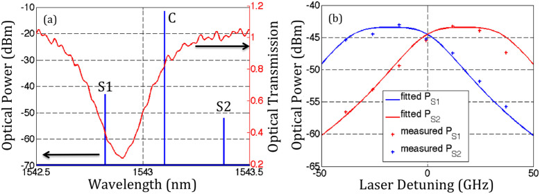
Figure 3. Recorded and predicted side bands generated by 35 GHz RF modulation at different laser detunings.
(a) shows an example of spectrum recorded with a high-resolution OSA at a laser detuning of -24.6 GHz. The carrier (C) and two asymmetric sidebands (S1 and S2) are clearly visible. The plot is overlaid with the optical transmission spectrum of the ring to illustrate that the enhanced sideband is closer to the resonance. (b) Summary of the power generated in the sidebands as a function of laser detuning. Modulation with a detuned RRM results in asymmetric side bands adequately modeled by equation (4).
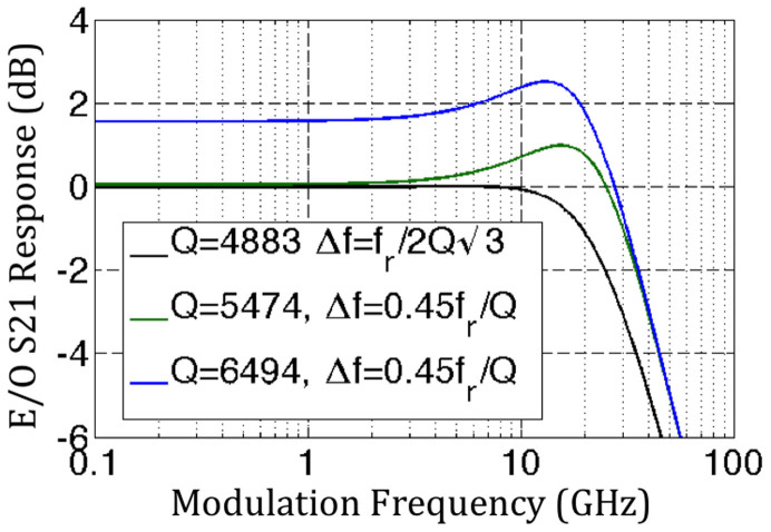
Figure 4. Comparison between calculated S-parameters for different Q-factors and laser detunings.
The black curve corresponds to the laser detuning expected to be the optimum based on a quasi-static analysis of the RRM, while the green and blue curves correspond to enhancement of either the bandwidth (green curve) or the modulation efficiency (blue curve) reoptimized taking peaking into account. All curves are normalized relative to the DC modulation efficiency of the black curve. Assumed Q-factors and laser detunings are indicated in the legend.
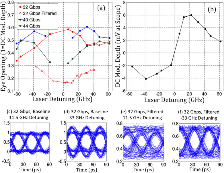
Figure 5. Recorded RRM eye diagrams evidencing peaking enhancement.
(a) Eye openings for different laser detunings at 32, 40 and 44 Gbps. At 32 Gbps, a second dataset was taken with additional penalization of the link (“filtered link”) introduced by a long, low grade SMA cable (−8 dB attenuation at 16 GHz modulation frequency). Eye openings are normalized to unit DC modulation efficiency. (b) summarizes the recorded DC modulation efficiency at different laser detunings. (c–f) show examples of individual eye diagrams in a penalized and non-penalized 32 Gbps link at low laser detuning (and thus small peaking) and moderate laser detuning (and high peaking). Here too, signal levels are normalized to unit DC modulation efficiency. Eye diagrams were recorded with PRBS 7 signals and 2 Vpp. Maximum signal levels in (e–f) are below one since the longest strings of consecutive zeros and ones were too short to fully reach stabilized DC levels. Eye diagrams are pattern lock averaged with a trigger generated every time the PRBS sequence is restarted, correctly representing ISI but averaging out receiver noise extrinsic to the RRM.
Figure 6. Circuit diagram of an idealized peaking amplifier with identical transfer function as the RRM.
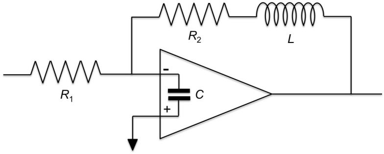
Corresponding values of the lumped electrical elements for the transfer functions shown in fig. 2 are given in the supplementary information. Since peaking amplifiers are a commonly used building block in high-speed communication systems, this equivalent circuit makes the characteristics of the RRMs directly accessible to system architects.
Results
Analytical modeling and experimental verification of peaking and asymmetric sideband generation
The investigated RRM (fig. 1) has a radius of 10.3 μm and is constituted out of a 400 nm wide ridge waveguide partially etched into the 220 nm thick silicon device layer of a silicon-on-insulator wafer with a remaining silicon slab height of 90 nm around the waveguide. A reversed biased PIN junction with nominal implant concentrations p− = 3e17 cm−3 and n− = 1e17 cm−3 overlapping by 50 nm serves as phase shifter. Electrical connectivity is obtained via highly doped regions with p+ and n+ = 1e20 cm−3. The total junction capacitance is 17 fF at −1 V bias and the series resistance 215Ω, resulting in an electrically limited RC-bandwidth of 43 GHz (details of the phase shifter can be found in ref. 11).
In order to derive the optical response of the modulator, we start with the equations introduced in refs. 36,38
 |
 |
where a is the amplitude of the field travelling inside the resonator, ωr the (angular) resonant frequency of the resonator, τa the 1/e decay time of the field amplitude (including both waveguide and coupling losses), μ the coupling strength between the resonator and the bus waveguide and t the time. EIn and EOut are the amplitude of the waveguide mode incoming towards and outgoing from the modulator (fig. 1(b)). The time-domain coupling parameter μ verifies μ2 = κ2νg/L, where κ is the waveguide coupling parameter at the junction to the resonator, vg the group velocity of the waveguide constituting the ring and L its circumference. By applying the sinusoidal drive voltage δV·sin(ωmt) the resonant frequency of the resonator is shifted to ωr + δωr·sin(ωmt), where the nonlinearity of the transfer function is neglected since we are deriving the small signal S-parameter. We do assume however that δωr is a complex number with the imaginary part taking into account the modulation of the free-carrier induced losses that necessarily accompanies the index modulation39. The inclusion of this effect is necessary to describe the asymmetry of the recorded S21 for laser detuning to the left versus to the right of the ring resonance (fig. 2).
Equation (1) implies that a resonant frequency shift applied to the resonator is tracked by the light stored inside the resonator, i.e., preexisting light inside the resonator oscillates within the latter at its natural resonance frequency in the absence of additional light coupled from the waveguide (in analogy to a driven harmonic oscillator with damping ratio 1/τaωr, the incoming optical carrier playing the role of the driving force). The corresponding wavelength change is allowed by the broken time invariance of the externally driven resonator40, an effect that has been experimentally verified41. By assuming δV and δωr to be small quantities and applying first order perturbation theory (complete derivation in the supplementary information) we derive the small signal response of the modulator to be
 |
where S21,EO is the electro-optic S21 (on a linear scale), ω0 is the frequency of the continuous wave optical carrier incoming from the laser,  , and
, and  is the value of a in the absence of modulation voltage, i.e., its average or DC value
  .
.
Measured E/O S21 were fitted with equation (3) for a complete set of laser wavelengths spanning the entire resonance linewidth of the ring, with an excellent agreement between theory and experiment (fig. 2). The fitted change of photon lifetime versus resonance shift  , 0.13, is higher (2×) but still reasonably close to the calculated value based on free carrier absorption and refractive index shift coefficients reported in the literature for bulk silicon39,42 (supplementary information). The Q-factors (3500 to 5000 depending on the wavelength) and waveguide coupling strengths were extracted from the experimental data. The laser detuning had to be corrected for thermal effects, i.e., it corresponds to the detuning between the frequency of the laser and the resonance of the ring as thermally shifted at the specific laser power and frequency. This was determined by comparing the thermally distorted optical transfer function of the ring to a transfer function recorded at low optical power featuring a near-perfect lorentzian line shape and mapping the points with corresponding extinction (see methods section). With the exception of a residual laser detuning below a few picometers due to drift during the measurements and of ϑ, there were no fitted parameters. A description of the de-embedding procedure used to calibrate the S21 curves for RF losses occurring outside of the device can be found in the methods section.
The two additive terms of equation (3) correspond to the generation of two side lobes with asymmetric magnitudes
 |
a prediction that was also confirmed by experiment and fitted with the same methodology as the E/O S21 (fig. 3).
Peaking occurs when the modulation frequency ωm is close to the detuning of the laser frequency ω0 relative to the cavity resonance ωr, i.e., ωm = ±(ωr − ω0). Of the two sidebands, the sideband generated closest to resonance is also asymmetrically enhanced under these conditions. Peaking becomes more pronounced at large laser detuning on the order of or larger than 1/2πτa, since the peaking frequency is then sufficiently far from DC for the peak to be resolved. A physical explanation in terms of time constants is given in the following.
As pointed out before12, overshoot in optical RRMs is the result of an interference effect between the light inside the modulator and the incoming light from the waveguide with a beating frequency given by the laser detuning. A perturbation theoretical treatment of the problem gives further insight into the physical mechanism: The response of the optical amplitude inside the ring resonator, δa, to the resonant frequency shift, δωr, verifies
 |
In other words, the resonance frequency shift acts as a source term for δa after which the generated perturbation continues to oscillate at the natural resonator frequency ωr rather than the frequency of the incoming optical carrier ω0 (in the previously introduced analogy of a driven oscillator, the additional oscillation generated by a sudden perturbation δωr continues to oscillate at the natural frequency of the oscillator rather than the frequency of the driving force). Close to resonance, the light propagating inside the resonator normally couples back to the bus waveguide with a destructive interference relative to the incoming light, leading to the extinction seen at resonance in the optical transfer function of the RRM43 (the destructive interference can e.g. be derived from the fact that the coupling parameter between ring and waveguide is in quadrature to the junction transmission coefficient so that two coupling events from the waveguide to the resonator and back result in a −1 sign). A positive step perturbation δωr results in δa being generated with a π/2 phase advance relative to a (term −iδωr(t)a in equation (5)). δa then continues to oscillate at the natural resonator frequency ωr with a detuning ωr − ω0 relative to the optical carrier. After a time delay π/2(ωr − ω0), an additional π/2 phase advance is accumulated and the destructive interference condition converts into a constructive one, i.e., δa couples constructively to the waveguide, resulting in an excess power coupled out of the cavity and an overshoot in the modulator response. A prerequisite for this to occur is of course that the perturbation δa has not yet decayed, i.e., the time for the dephasing to occur, π/2(ωr − ω0), has to be shorter than the photon lifetime inside the cavity (τa). The overshoot results in an enhancement of the modulator response (S21) at RF frequencies close to ωr − ω0: If one considers for example a square wave electrical drive signal with a period ωr − ω0, the overshoot occurs exactly halfway between the falling edge (rising δωr) and the rising edge (falling δωr), boosting the electrical “0”-level (optical “1”-level due to data inversion when ωr > ω0). The same reasoning can be applied for a laser detuning corresponding to a negative ωr − ω0, in which case δa is generated with a π/2 phase retardation for a negative step perturbation δωr (rising edge of the electrical square wave) that is also converted to a π dephasing after an additional π/2(ωr − ω0) time delay, boosting the electrical “1”-level (also optical “1”-level). In summary, the interference between a and δa results in ringing with a frequency |ω0−ωr| in the response of the RRM to a short pulse, so that periodic driving of the RRM at a frequency ωm = |ω0−ωr| synchronized with the impulse response of the ringing leads to an enhanced S21 (peaking).
Application to ISI reduction in ultra-high-speed optical links
The peaking predicted and experimentally verified in the previous section can be used to enhance the characteristics of RRMs, with the possibility of either enhancing the bandwidth of the device or its drive voltage/RF power consumption depending on the priorities driven by the system architecture. Numerical examples are first given based on the model derived in the previous section. The effect is then experimentally verified with measured eye diagrams.
At low frequencies, the maximum response of a critically coupled RRM is obtained for a laser detuning of  (see supplementary information). Further detuning of the laser results in a reduction of the DC response, but also results in an extended bandwidth via peaking and can increase the eye opening at high data rates. The optimum laser detuning depends on the data rate and can be deduced from equation (3) together with the S-parameters of the rest of the system. In order to exemplify this, we calculated E/O S-parameters for different Q-factors and laser detunings that illustrate how either power consumption, drive voltage or bandwidth can be improved via the RRM peaking.
Figure 4 shows a comparison between E/O S-parameters calculated for different Q-factors and laser detunings. The other parameters are identical to the ones used to model the experimental results in fig. 2 (in particular, the phase tuner's phase shift is assumed to remain unchanged and critical coupling is assumed to be maintained). The black curve corresponds to a laser detuning of  resulting in the highest low speed modulation efficiency given the assumed Q-factor (4883) and no noticeable peaking. The green curve corresponds to an increased Q-factor (5474) with the resulting decrease in E/O bandwidth overcompensated by a larger laser detuning
  and a stronger peaking. The DC modulation efficiency is the same (the higher Q-factor is compensated by the larger detuning), but the bandwidth is increased from 30 GHz to 40 GHz when referenced to the −3 dB level below the DC S21 and to 35 GHz when referenced to −3 dB level below the peak of the S21 curve. The blue curve also corresponds to
  , with a Q-factor further increased to 6494. The E/O bandwidth drops back to its initial level (33 GHz when referenced to the DC S21, 29 GHz when referenced to the peak of the S21), but the DC S21 is enhanced by 1.56 dB (defined as 20log10(OMA)). It should be noted that referencing the 3 dB roll-off to the peak of the S21 is the more conservative and fairer metric, since peaking also introduces phase distortion. It can be concluded from these curves that optimizing the laser detuning for maximum DC modulation amplitude, as would be the natural choice when peaking is ignored, is suboptimal in either case. A systematic experimental study of the modulation efficiency/modulation bandwidth trade-off based on equation (3) can be found in ref. 35, albeit critical coupling was not maintained.
Figure 5 shows examples of eye diagrams and summarizes eye openings recorded with the investigated RRM at different laser detunings and data rates, exemplifying the benefits of peaking in complete optical links. The baseline 32 Gbps link summarized by the solid red curve in fig. 5(a) is far from being bandwidth limited and the transient ringing corresponding to the S-parameter peaking in the time domain partially closes the eyes instead of opening them. At higher data rates, however, the optical links are bandwidth limited and the peaking contributes to extending the bandwidth of the link and reopening the eyes. At 40 Gbps, the eyes could for example be reopened to the same level as in the baseline 32 Gbps link. The optimum peaking depends on the data rate, with the optimum laser detuning increasing at higher data rates. Similarly, the peaking can also contribute to recovering good performance in a link that is heavily bandwidth limited due to other components. To exemplify this, we recorded eye diagrams after penalizing the 32 Gbps link with an additional low grade SMA cable (−8 dB attenuation at the Nyquist frequency, 16 GHz). A substantial peaking enhancement of the optical link then also becomes visible. Figures 5(c)–(f) are examples of 32 Gbps eye diagrams with and without extrinsic penalization, as well as with low and high peaking. In case of the baseline 32 Gbps link, peaking is clearly visible in the form of an overshoot of rapidly changing data patterns (fig. 5(d)), while in the penalized 32 Gbps optical link peaking is visible in the form of a reopening of the eye diagram (fig. 5(f)). A net enhancement of the absolute OMA cannot be observed in this dataset (i.e., the product of the data shown in figs. 5(a) and 5(b)) because even for the most highly penalized link shown in fig. 5 (dashed red curve in (a) and eye diagrams (e) and (f)), the eye diagram is already completely reopened at −33 GHz detuning (fig. 5(f)) making further bandwidth enhancement unnecessary and detuning beyond the DC OMA optimum detrimental. Such an effect is however expected to be apparent in more heavily filtered links or with higher Q-factor RRMs optimized for lower speeds.
In order to leverage the peaking in a communication system architecture, it is useful to describe the response of the RRM with a well-known equivalent electric circuit, facilitating the work for system architects not familiar with the intricacies of this device. The idealized peaking amplifier shown in fig. 6 actually has exactly the same transfer function for adequately chosen electrical components. Equation (3) can be recast into
 |
where  and Δω = ω0 − ωr is the laser detuning. This then takes the same form as the transfer function of a peaking amplifier
 |
where VIn and VOut are the input and output voltages of the amplifier, R1, R2, C and L are the lumped element electrical components shown in fig. 6 and Av is the voltage gain of the operational amplifier (note that equation (7) is complex conjugated compared to the usual convention used in electronics to make it consistent with the convention for time dependence as exp(−iωt) used here and elsewhere in the paper).
Discussion
We have modeled the transient E/O response of RRMs with a closed form expression derived with perturbation theory that predicts both peaking in the S-parameter as well as asymmetrically generated side bands. The de-embedding methodology developed for the characterization of the RRMs allows the determination of the E/O response of the RRM with sufficient precision to enable a one to one comparison with the theoretical RRM response. Both predictions are verified experimentally with excellent agreement. The impact of peaking on ISI reduction in RRM based optical links is demonstrated based on the reopening of eye diagrams at high data rates as well as in transmission systems penalized elsewhere in the link. An equivalent circuit description of the RRM allows straightforward evaluation of this effect on optical datacom links with existing system analysis methodologies.
The results reported in this paper show that complex time dynamics need to be taken into account when interpreting measurement data and optimizing RRM designs even for the well-known lumped element RRMs relying on resonant frequency modulation. Simple models reducing the time dynamics of RRMs to a single pole filter resulting from the photon lifetime in the cavity fail to account for the actual response of the devices. In particular, leveraging peaking in a communication system architecture allows moderately increasing the quality factor of the RRMs without compromising data integrity, thus reducing the drive voltage and the power consumption and is thus an important aspect for device performance. Given the relative simplicity of the closed form expression derived for the E/O RRM response, taking RRM time dynamics into account in future communication system architectures should be greatly facilitated.
Methods
De-embedding of the E/O S21
The RRM is connected to two GSG pad frames, one serving as an input and one serving as a 50Ω terminated output, both being accessed with 40 GHz rated probe tips. The entire setup was based on K-type connectors rated up to 46 GHz. Both the E/O S21 and the electrical S21 of the chip were measured; the latter defined as the transmission from the input pad frame to the output pad frame. The on-chip signal traces between either of the two pad frames and the RRM are of different lengths (fig. 7), resulting in the measured RRM bandwidth depending on the pad frame used as the input port. In addition to normalizing out the cable attenuation and the S-parameter of the receiver used in the test setup, following procedure was employed to de-embed the on-chip RF attenuation: First the device was measured by injecting the RF signal into pad frame A and normalizing the S21 relative to the electrical signal level arriving at pad frame A obtained by subtracting cable losses from the VNA output (source). This underestimates the S21 by the amount of electrical signal losses occurring between pad frame A and the modulator (S21(InA, NormA)). In a second measurement, the signal was injected into pad frame B, while pad frame A served as the 50Ω terminated chip output. The measurement was normalized by a different method, relative to the electrical signal level at the output pad frame of the chip obtained by normalizing out cable losses from the signal received at the VNA input (sink) used to measure the electrical S21. This overestimates the S21 by the same amount, i.e., the electrical signal losses between pad frame A and the modulator (S21(InB, NormA)). The de-embedded signal was then taken as the mean of the two datasets, since they respectively overestimate and underestimate the O/E S21 by the same amount (fig. 8). This method proved to be extremely reliable up to 35 GHz. Swapping the role of pad frames A and B in both measurements resulted in the same de-embedded S21. In addition, to validate the methodology, we compared the on-chip signal losses extracted from O/E measurements S21(InA, NormA)-S21(InB, NormB) with the on-chip signal losses obtained directly from the electrical S21, with excellent consistency up to 35 GHz (fig. 9(a)). Beyond this point, there is a sharp difference between the directly measured electrical signal loss and the dataset extracted from the O/E measurements attributed to strong RF reflections at the chip output pads. These reflections were independently confirmed with the electrical S11 of the chip (fig. 9(b)). They lead to a sharp enhancement or penalization of the measured E/O S-parameter depending on which pad frame is used as an output, which is attributed to a RF node or antinode forming at the RRM depending on the distance to the pad frame. In particular, the additional drop-off relative to the predicted S21 does not follow the single pole dependency associated to the intrinsic electrical bandwidth of the modulator. It should also be noted that while this de-embedding procedure may appear intricate, it is only a minor refinement: Pad frame A is much closer to the modulator than pad frame B, so that very small losses occur between these two elements. Taking pad frame A as an input and normalizing the S21 relative to the electrical signal level arriving at pad frame A results in almost the same S21, within 1.5 dB up to 35 GHz (fig. 8). S-parameters were recorded with an Agilent 50 GHz VNA (N5245A) and a U2T high-speed photoreceiver (40 GHz bandwidth XPRV2021A). Eye diagrams were generated with an Anritsu 56 G pattern generator consisting of an MP1800 BERT System, 4 MU181020B 14 G pattern generators and an MP1821A MUX and recorded with a 50 GHz sampling oscilloscope from Agilent (83484A). Sideband measurements were done with a high resolution OSA from APEX (AP2043B) resolving 5 MHz optical frequency.
Figure 7. Snapshot of the mask definition.
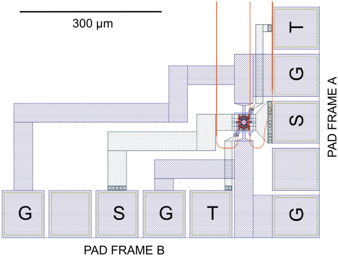
Pad frames A and B referenced in the text are marked. Pads labeled by G, S and T are respectively ground pads, signal pads and pads used to apply a control signal to thermally tune the rings. Waveguides are shown in orange.
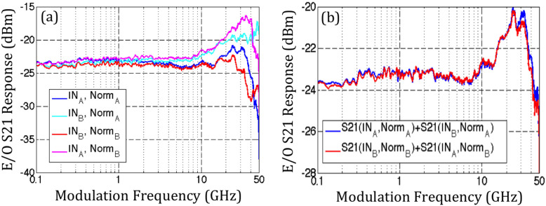
Figure 8. Example of datasets taken with different test setup configurations and resulting de-embedded S-parameter.
(a) shows the four measurement configurations, with electrical signals injected either through pad frame A or B (INA and INB) and S21 curves normalized relative to the signal levels at either pad frame (NormA and NormB). (b) shows the averaged S-parameters obtained with two different configurations, with excellent consistency obtained between the two datasets.
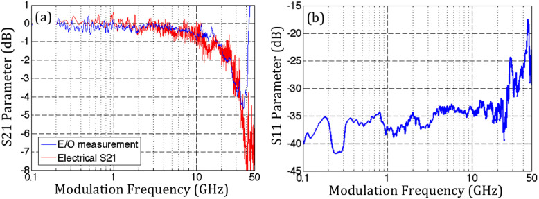
Figure 9. Comparison between the on-chip losses extracted from the E/O measurements to a direct measurement of the electrical S21 of the chip (a) and measured back-reflections at the chip input (b).
We attribute the strong increase in the dataset extracted from the difference of measured E/O responses in (a) to the increased RF back-reflections seen in (b) above 35 GHz, as explained in the text.
Figure 7 shows a snapshot of the chip layout. Two pad frames enable electrical connectivity to GSG signal lines, with one pad frame used to inject the signal from the VNA and the other to return the signal to the VNA, both 50Ω terminating the chip and allowing recording the electrical S21 of the chip. De-embedding the signal attenuation occurring in the SMA cables used in the test setup is straightforward since their S-parameters are directly accessible. Signal attenuation on the chip however also plays a role and is harder to de-embed. While measuring the electro-optic response of the RRM by injecting the electrical signal through the pad frame with the shorter signal lines (pad frame A) and taking into account the cable losses between the VNA and the chip input already results in quite accurate results (within 1.5 dB of the more accurate de-embedding procedure described here), we were able to obtain more accurate results by taking several measurements into account obtained with different test setup configurations.
Figure 8 shows examples of the four datasets corresponding to the different input pads and normalizations. As explained above, S21(InA,NormA) underestimates the E/O S-parameters by the amount of electrical attenuation between pad frame A and the RRM, while S21(InB,NormA) overestimates the E/O S-parameter by the same amount. Thus the average of the two curves is a good estimate of the de-embedded E/O S21. Normalizing relative to the signal levels at pad frame B increases the error, since the attenuation between the pad frame and the device is higher due to the longer signal traces. However, averaging the two curves S21(InB,NormB) and S21(InA,NormB) again averages out the opposing measurement biases and results in the same de-embedded curve than previously (fig. 8(b)). Consistency between these two procedures indicates that the de-embedding methodology is adequate.
In order to independently verify the adequacy of the de-embedding procedure, a simple test can be made consisting in comparing the on-chip losses extracted from the difference between raw E/O S-parameters taken by injecting the electrical signal into either pad frame A or pad frame B to the on-chip RF losses directly extracted from the electrical S21. The comparison between the two curves can be seen in fig. 9. It is apparent that up to 35 GHz modulation frequency the consistency is excellent, confirming that up to this point on-chip signal distortion is primarily due to attenuation. At higher frequencies, there is a sharp discrepancy seen in the data extracted from the E/O S21.
This discrepancy is attributed to RF reflections induced at the pad frame or the probe tip at the output of the chip. Indeed, the reflected RF wave can add-up constructively or destructively to the forward propagating wave at the RRM, either boosting or reducing the observed S21. The effect of such a back-reflection is thus sensitive to the electrical path length between the output pad frame and the device. The reflections are further confirmed by directly measuring the electrical power returning to the VNA. As seen in fig. 9(b), S11 grows substantially above 35 GHz. It can be concluded from the entire dataset that the de-embedding procedure works extremely well up to 35 GHz modulation frequency, after which RF reflections play a dominant role.
Thermal effects on the effective laser detuning
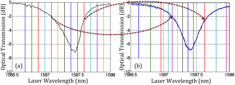
A second effect that needs to be carefully taken into account is the thermal resonance shift of the RRM induced by optical absorption in the ring. Since the amount of absorbed optical power, and thus the amount of self-heating and thermal shift, depends on the detuning of the laser, a separate corrective factor needs to be applied for every laser wavelength. The required corrective factors could be straightforwardly experimentally determined by comparing a ring resonance recorded under the same conditions as the E/O responses (10 dBm in the waveguide) to the same resonance recorded at low optical power levels with negligible non-linearity (-6 dBm in the waveguide). As is illustrated in fig. 10, points in the transfer functions with identical extinction are mapped to each other. The effective laser detuning is then taken as the detuning in the mapped diagram (dataset with a lorentzian line shape recorded at low optical power levels). Since thermal effects are too slow to track the ring dynamics at the recorded modulation frequencies, the resonant frequency of the ring can be considered as being simply DC shifted during the RF measurements.
Figure 10. Comparison of the ring transfer function recorded at high (10 dBm in waveguide) and low (−6 dBm in waveguide) optical power levels and determination of the laser detuning relative to the thermally shifted resonant frequency.
The laser detuning read from (b) after mapping is also the actual laser detuning relative to the thermally shifted resonance for (a) and is the detuning taken into account in the fitting of the experimental results. The transfer function in (b) is overlaid with a fit corresponding to an ideal ring model (i.e., without thermal effects).
Author Contributions
J.W. conceived the experiments and derived the theory, F.M. and S.R.G. designed the device, J.M. and S.S.A. measured the device, J.M. and J.W. analyzed the data, J.H. and B.S. contributed to the test setup, J.W. wrote the paper.
Supplementary Material
Supplementary Information
Acknowledgments
The authors gratefully acknowledge funding from the European Research Council (FP7/2011-2016 279770) for the project “Frontiers of Integrated Silicon Nanophotonics in Telecommunications” and from the European Commission under contracts 293767 and 619591 for the projects “Silicon Photonics Coherent Optical Wavelength Division Multiplexed Transceiver” and “Broadband Integrated and Green Photonic Interconnects for Higher-Performance Computing and Enterprise Systems”. The chips were fabricated at the Singapore Institute of Microelectronics (IME) via the shuttle service OpSIS.
References
- Rabiei P., Steier W. H., Zhang C. & Dalton L. R. Polymer Micro-Ring Filters and Modulators. J. Lightwave Technol. 20, 1968 (2002). [Google Scholar]
- Xu Q., Schmidt B., Pradhan S. & Lipson M. Micrometer-scale silicon electro-optic modulator. Nat. 435, 325–327 (2005). [DOI] [PubMed] [Google Scholar]
- Dong P. et al. Low Vpp, ultralow-energy, compact, high-speed silicon electro-optic modulator. Opt. Express 17, 22484–22490 (2009). [DOI] [PubMed] [Google Scholar]
- Gardes F. Y. et al. High-speed modulation of a compact silicon ring resonator based on a reverse-biased pn diode. Opt. Express 17, 21986–21991 (2009). [DOI] [PubMed] [Google Scholar]
- Li G. et al. 25Gb/s 1V-driving CMOS ring modulator with integrated thermal tuning. Opt. Express 19, 20435–20443 (2011). [DOI] [PubMed] [Google Scholar]
- Xiao X. et al. 44-Gb/s Silicon Microring Modulators Based on Zigzag PN Junctions. Photon. Technol. Lett. 24, 1712–1714 (2012). [Google Scholar]
- Arakawa Y., Nakamura T., Urino Y. & Fujita T. Silicon Photonics for Next Generation Integration Platform. IEEE Commun. Mag. 51, 72–77 (2013). [Google Scholar]
- Jalali B. & Fathpour S. Silicon Photonics. J. Lightwave Technol. 24, 4600–4615 (2006). [Google Scholar]
- Xu Q., Manipatruni S., Schmidt B., Shakya J. & Lipson M. 12.5 Gbit/s carrier-injection-based silicon micro-ring silicon modulators. Opt. Express 15, 430–436 (2007). [DOI] [PubMed] [Google Scholar]
- Thomson D. J. et al. 50-Gb/s Silicon Optical Modulator. Photon. Technol. Lett. 24, 234–236 (2012). [Google Scholar]
- Merget F. et al. Silicon photonics plasma-modulators with advanced transmission line design. Opt. Express 21, 19593–19607 (2013). [DOI] [PubMed] [Google Scholar]
- Xu Q., Schmidt B., Shakya J. & Lipson M. Cascaded silicon micro-ring modulators for WDM optical interconnection. Opt. Express 14, 9431–9435 (2006). [DOI] [PubMed] [Google Scholar]
- Lelarge F. et al. Recent Advances on InAs/InP Quantum Dash Based Semiconductor Lasers and Optical Amplifiers Operating at 1.55 μm. J. Select. Topics. Quantum Electron. 13, 111–124 (2007). [Google Scholar]
- Gubenko A. et al. Error-free 10 Gbit/s transmission using individual Fabry-Perot modes of low-noise quantum-dot laser. Electron. Lett. 43, 1430–1431 (2007). [Google Scholar]
- Del'Haye P. et al. Optical frequency comb generation from a monolithic microresonator. Nat. 450, 1214–1217 (2007). [DOI] [PubMed] [Google Scholar]
- Razzari L. et al. CMOS-compatible integrated optical hyper-parametric oscillator. Nat. Photonics 4, 41–45 (2010). [Google Scholar]
- Levy J. S. et al. CMOS-compatible multi-wavelength oscillator for on-chip optical interconnects. Nat. Photonics 4, 37–40 (2010). [Google Scholar]
- Pfeifle J. et al. Coherent data transmission with microresonator Kerr frequency combs. Nat. Photonics 8, 375–380 (2014). [DOI] [PMC free article] [PubMed] [Google Scholar]
- Padmaraju K. et al. Error-free transmission of microring-modulated BPSK. Opt. Express 20, 8681–8688 (2012). [DOI] [PubMed] [Google Scholar]
- Xie X., Khurgin J., Kang J. & Chow F.-S. Linearized Mach-Zehnder Intensity Modulator. Photon. Technol. Lett. 15, 531–533 (2003). [Google Scholar]
- Gutierrez A. M. et al. Ring-Assisted Mach-Zehnder Interferometer Silicon Modulator for Enhanced Performance. J. Lightwave Technol. 30, 9–14 (2012). [Google Scholar]
- Gould M. et al. Silicon-polymer hybrid slot waveguide ring-resonator modulator. Opt. Express 19, 3952–3961 (2011). [DOI] [PubMed] [Google Scholar]
- Shainline M. J. et al. Depletion-mode polysilicon optical modulators in a bulk complementary metal-oxide semiconductor process. Opt. Lett. 38, 2729–2731 (2013). [DOI] [PubMed] [Google Scholar]
- Miller D. A. B. Energy consumption in optical modulators for interconnects. Opt. Express 20, A293–A308 (2012). [DOI] [PubMed] [Google Scholar]
- Watts M. R., Zortman W. A., Trotter D. C., Young R. W. & Lentine A. L. Vertical junction silicon microdisk modulators and switches. Opt. Express 19, 21989–22003 (2011). [DOI] [PubMed] [Google Scholar]
- Teng J. et al. Athermal Silicon-on-insulator ring resonators by overlaying a polymer cladding on narrowed waveguides. Opt. Express 17, 14627–14633 (2009). [DOI] [PubMed] [Google Scholar]
- Dong P. et al. M. Thermally tunable silicon racetrack resonators with ultralow tuning power. Opt. Express 18, 20298–20304 (2010). [DOI] [PubMed] [Google Scholar]
- Melikyan A. et al. High-speed plasmonic phase modulators. Nat. Photonics 8, 229–233 (2014). [Google Scholar]
- Manipatruni S., Preston K., Chen L. & Lipson M. Ultra-low voltage, ultra-small mode volume silicon microring modulator. Opt. Express 18, 18235–18242 (2010). [DOI] [PubMed] [Google Scholar]
- Gill D. M. et al. Internal Bandwidth Equalization in a CMOS-Compatible Si-Ring Modulator. Photon. Technol. Lett. 21, 200–202 (2009). [Google Scholar]
- Gill D. M. et al. CMOS-Compatible Si-Ring-Assisted Mach-Zehnder Interferometer With Internal Bandwidth Equalization. J. Select. Topics Quantum Electron. 16, 45–52 (2010). [Google Scholar]
- Bortnik B. et al. Electrooptic polymer ring resonator modulation up to 165 GHz. J. Select. opics Quantum Electron. 13, 104–110 (2007). [Google Scholar]
- Sacher W. D. et al. Coupling modulation of microrings at rates beyond the linewidth limit. Opt. Express 21, 9722–9733 (2013). [DOI] [PubMed] [Google Scholar]
- Yu H. et al. Trade-off between optical modulation amplitude bandwidth of silicon micro-ring modulators. Opt. Express 22, 15178–15189 (2014). [DOI] [PubMed] [Google Scholar]
- Sharif Azadeh S. et al. Advances in Silicon Photonics Segmented Electrode Mach-Zehnder Modulators and Peaking Enhanced Resonant Devices. Proc. SPIE 9288 (2014). In press. [Google Scholar]
- Little B. E., Chu S. T., Haus H. A., Foresi J. & Laine J.-P. Microring Resonator Channel Dropping Filters. J. Lightwave Technol. 15, 998–1005 (1997). [Google Scholar]
- Sacher W. D. & Poon J. K. S. Dynamics of microring resonator modulators. Opt. Express 20, 15741–15753 (2008). [DOI] [PubMed] [Google Scholar]
- Zhang L. et al. Silicon-based Microring Resonator Modulators for Intensity Modulation. J. Select. Topics Quantum Electron. 16, 149–158 (2010). [Google Scholar]
- Soref R. A. & Bennett B. R. Electrooptical Effects in Silicon. J. Quantum Electron. 23, 123–129 (1987). [Google Scholar]
- Notomi M. & Mitsugi S. Wavelength conversion via dynamic refractive index tuning of a cavity. Phys. Rev. A 73, 051803 1–4 (2006). [Google Scholar]
- Preble S. F., Xu Q. & Lipson M. Changing the color of light in a silicon resonator. Nat. Photonics 1, 293–296 (2007). [Google Scholar]
- Lin Q., Painter O. J. & Agrawal G. P. Nonlinear optical phenomena in silicon waveguides: Modeling and applications. Opt. Express 15, 16604–16644 (2007). [DOI] [PubMed] [Google Scholar]
- Yariv A. Critical Coupling and Its Control in Optical Waveguide-Ring Resnator Systems. Photon. Technol. Lett. 14, 483–485 (2002). [Google Scholar]
Associated Data
This section collects any data citations, data availability statements, or supplementary materials included in this article.
Supplementary Materials
Supplementary Information


