Abstract
We report investigations on the influences of post-deposition treatments on the performance of solution-processed methylammonium lead triiodide (CH3NH3PbI3)-based planar solar cells. The prepared films were stored in pure N2 at room temperature or annealed in pure O2 at room temperature, 45°C, 65°C and 85°C for 12 hours prior to the deposition of the metal electrodes. It is found that annealing in O2 leads to substantial increase in the power conversion efficiencies (PCEs) of the devices. Furthermore, strong dependence on the annealing temperature for the PCEs of the devices suggests that a thermally activated process may underlie the observed phenomenon. It is believed that the annealing process may facilitate the diffusion of O2 into the spiro-MeOTAD for inducing p-doping of the hole transport material. Furthermore, the process can result in lowering the localized state density at the grain boundaries as well as the bulk of perovskite. Utilizing thermal assisted O2 annealing, high efficiency devices with good reproducibility were attained. A PCE of 15.4% with an open circuit voltage (VOC) 1.04 V, short circuit current density (JSC) 23 mA/cm2, and fill factor 0.64 had been achieved for our champion device.
The dramatic emergence of the hybrid inorganic-organic perovskites as a photovoltaic material resulted in a remarkable impact on the field of photovoltaics1,2,3. Such impressive progress in the development of the perovskite-based photovoltaic cells is attributed to the desirable physical properties for this class of materials such as their broadly tunable bandgaps4, high absorption coefficients over a wide range of visible light spectrum5, extremely long carrier diffusion lengths6,7, good crystallinity8,9 and high carrier mobilities9,10,11, which have fulfilled most of the criteria required for manufacturing high efficiency solar cells. Starting from the first attempt of using perovskite as the sensitizer12 for solar cells in 2009, the PCEs of perovskite-based devices have been enhanced from 3.8%12 to around 15%13,14, which represents the most rapid rate of increase in recent years compared to other competing photovoltaic technologies. During the time of the composition of this paper, the PCEs of perovskite solar cells have been further boosted to 16.2% (certified) and 19.3% by the efforts of Jeon et al.15 and Zhou et al.16 With continuing development of the perovskite-based solar cells, the device efficiency which is comparable to the commercial single-crystalline silicon solar cells potentially can be achieved in the near future.
CH3NH3PbI3, with a bandgap of 1.5 eV, is the most studied perovskite-based photovoltaic material, which has been incorporated into different structures of electron injecting layers such as the compact titanium(IV) oxide (TiO2) layer17 and mesoporous TiO2 layer14,18,19,20,21 or combined with one-dimensional nanostructures such as TiO2 nanorods22, nanofibers23 and ZnO nanorods24,25,26 for the formation of high efficiency photovoltaic cells. Due to the fact that the architecture of the perovskite solar cells evolved from mesoscopic dye-sensitized solar cells (DSSCs), tremendous research efforts of employing perovskite absorbers have been initially focused on TiO2 mesostructures yielding PCEs as high as 15% for CH3NH3PbI3 based perovskite devices14. However, as demonstrated by M. M. Lee et al.8 and J. M. Ball et al.,27 high PCE can also be achieved even if the mesoporous TiO2 is replaced with an insulating alumina (Al2O3) mesoscopic scaffold. Due to the higher conduction band of Al2O3 compared to the lowest unoccupied molecular orbital (LUMO) of the perovskite layer, it is not possible for the electrons to be injected from the perovskite layer into the Al2O3 scaffold indicating that the photoexcited electrons are transported through the perovskite layer8. This discovery raises the question of whether the TiO2 mesostructure is necessary to achieve high efficiency perovskite solar cells. Recently, several research groups have demonstrated efficient perovskite solar cells in a planar structure without the mesoscopic scaffold13,17,28,29,30,31,32,33,34. This type of architecture allows for much simpler fabrication process, minimizes the chance of charge recombination at the interfaces and can be compatible with multijunction in hybrid tandem solar cells.
Among the published works, mixed halide perovskites13,32,33,34 (e.g. CH3NH3PbI3-xClx) or CH3NH3PbI317 are commonly employed in the planar structure with compact TiO2 as the hole blocking layer, yielding the highest PCE of 15.4% for vapor deposited CH3NH3PbI3-xClx-based device13 and 12.1% for CH3NH3PbI3-based device prepared by vapor-assisted solution process17. Although a number of reports have demonstrated significant potential in obtaining high efficiency perovskite-based solar cells, the group-to-group, or even batch-to-batch, variations in the reported PCEs is substantial which is believed to arise from the high sensitivity to the fabrication techniques and ambient during the formation of the active layers of the devices. Further development in the field of perovskite-based photovoltaics demands the establishment of a series of optimized and controllable fabrication procedures for yielding highly efficient and reproducible devices.
In this work, we have investigated planar heterojunction devices with a structure that consists of glass/fluorine-doped tin oxide (FTO)/TiO2 compact layer/CH3NH3PbI3/2,2′7,7′-tetrakis(N,N-di-p-methoxyphenyl-amine)-9,9′-spirobifluorene (spiro-MeOTAD)/molybdenum(VI) oxide (MoO3)/aluminum (Al) as illustrated in Fig. 1a. The perovskite films are prepared by sequential two- step solution processed deposition method14. Two post-deposition treatments were investigated. The devices were annealed in dry O2 for a period of 12 hours at 4 different temperatures: room temperature (ART); 45°C (A45); 65°C (A65); and 85°C (A85). An annealing time of 12 hours was chosen to ensure that the oxidation process is complete. The annealing time can be further optimized and has to be shortened to enhance the cost-effectiveness of the process. The control samples (NRT) were stored in N2 at room temperature for 12 hours before the deposition of metal electrodes. It is observed that the performances of perovskite-based devices are strongly affected by the post-deposition treatments of the films. Through careful control of the fabrication processes, a highest PCE of 15.4% was achieved. The processing conditions, post-deposition treatments and corresponding results will be discussed in detail, which are essential for the future development of perovskite-based solar cells.
Figure 1.
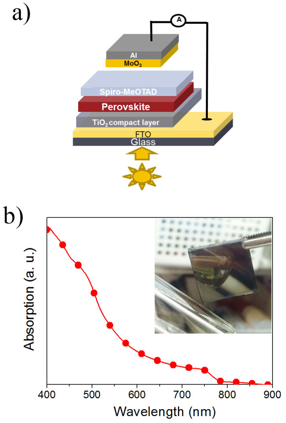
(a) The device architecture of CH3NH3PbI3 based solar cell (b) absorption spectra of CH3NH3PbI3 before and after O2 post-deposition treatments.
Results
CH3NH3PbI3-based solar cells have been fabricated and the device configuration is illustrated in Fig. 1a. The broad absorption spectrum of CH3NH3PbI3 is shown in Fig. 1b, indicating the strong photon harvesting capability of the material over the spectral range from 400 nm to 800 nm, which is in agreement with the band gap of 1.5 eV for CH3NH3PbI318,35. The inset of Fig. 1b is a photograph of a CH3NH3PbI3 film on the FTO coated glass substrate. The prepared film with smooth and reflective surface can be clearly observed by naked eyes, which is believed to be a desirable quality for the development of high performance devices31. The morphology and cross section of the samples have been investigated by scanning electron microscopy (SEM) and the images of typical films (A65) are presented in Fig. 2. From the plan-view image of CH3NH3PbI3 formed on TiO2 compact layer, crystalline domains of perovskite with grain size in the range of ~100 nm to ~800 nm with good surface coverage is observed. High surface coverage is of great importance for high performance devices as undesired shunting paths are minimized and thereby maximizing photo-carrier collection34. Furthermore, crystals with large grain size are shown to be favorable for charge transport17,36 and may serve as light scattering centers29 and are, therefore, preferable for the development of high performance devices. The cross-sectional SEM image of a typical device without the top electrode is shown in Fig. 2b. The thicknesses of the solution-processed CH3NH3PbI3 and spiro-MeOTAD layers are around 410 nm and 190 nm respectively, which are in the range of the reported values for achieving high efficiency devices8,14,19. The surface morphologies of PbI2 and CH3NH3PbI3 with or without the spiro-MeOTAD layer on top have been characterized by atomic force microscopy (AFM) and the results are shown in Fig. 3. It is found that the root mean square (RMS) roughness significantly increases from 25 nm to 31 nm after the PbI2 and the CH3NH3I layers were allowed to react to form CH3NH3PbI3. An increase in the grain size is observed subsequent to the formation of CH3NH3PbI3, which is attributed to the volume expansion17,37 commonly observed in the process. The surface roughness of CH3NH3PbI3 with the hole transport layer (HTL, spiro-MeOTAD) on top is reduced to 5 nm, indicating that the perovskite layer is fully covered and hence short-circuit currents due to the direct contact between the relatively conductive perovskite (~10−3 S cm−1) and metal electrode can be avoided8. The samples of CH3NH3PbI3 deposited on glass or compact TiO2 coated FTO substrates were further characterized by X-ray diffraction (XRD) and the diffraction patterns are shown in Fig. 4. Strong diffraction peaks located at 14.0°, 28.5° and 31.8° for 2θ scan were observed corresponding to the planes of (110), (220) and (310), which are in good agreement with the previous reports17,14,38, indicating that the tetragonal perovskite structure is formed5,12,37.
Figure 2.
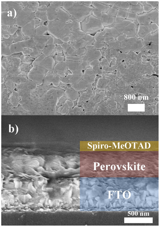
(a) Top-view and (b) cross-sectional SEM images for the sample of FTO/TiO2/CH3NH3PbI3/spiro-MeOTAD.
Figure 3.
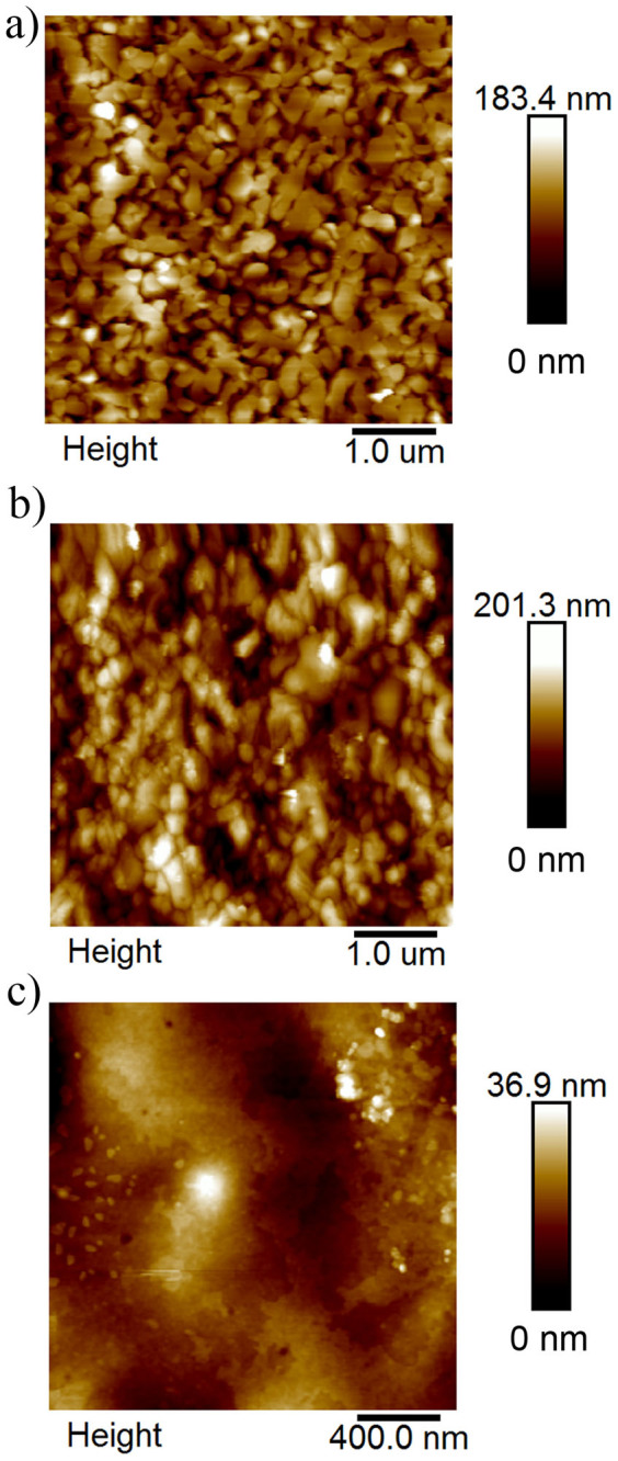
AFM images for (a) PbI2 (RMS: 25 nm) (b) CH3NH3PbI3 (RMS: 31 nm) and (c) CH3NH3PbI3/spiro-MeOTAD (RMS: 5 nm).
Figure 4.
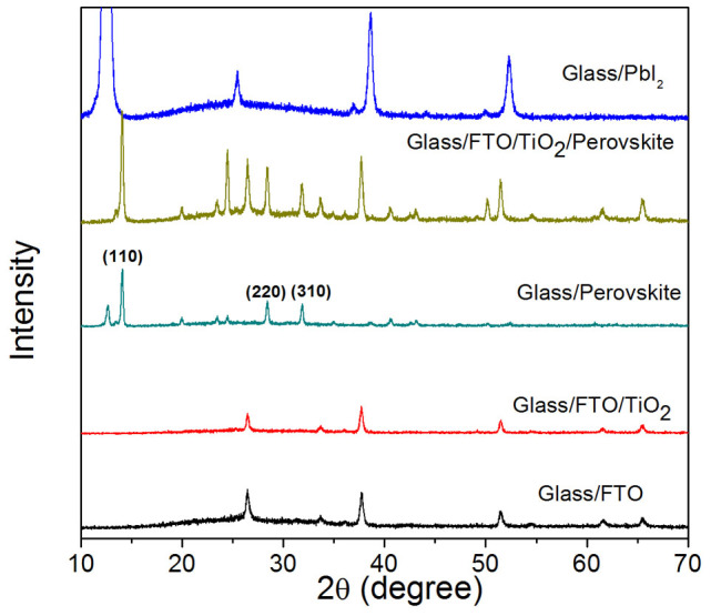
XRD patterns for the sample with different layers on glass or FTO coated glass.
The CH3NH3PbI3-based planar devices were fabricated in an N2-filled glove box (O2 and H2O <0.1 ppm) since the perovskite materials are easily decomposed in the presence of moisture39. However, we found that the devices exhibit poor performance when the entire fabrication processes were carried out in the glove box. This is attributed to the poor doping conditions for the spiro-MeOTAD layer as it was pointed out that O2 may be essential for the doping mechanism of spiro-MeOTAD40,41,42. We have performed I-V measurements on the spiro-MeOTAD film using the Transfer Length Method (TLM). Resistances across the electrodes with different separations are shown in Fig. 5. The results clearly indicate significant reduction in the resistance of the spiro-MeOTAD layer annealed in O2 ambient. This is indicative of improved doping level for the annealed film. Similar observations of reduction in the cell efficiency for solid-state dye-sensitized solar cells fabricated in N2 had also been reported previously42. This situation differs from the fabrication of organic devices, such as organic light emitting devices and organic solar cells, for which exposure to O2 should be avoided as it can lead to severe device degradation43,44. Considering the fact that moisture is highly devastating to the performance of perovskite-based devices while O2 is necessary for obtaining high efficiency devices, we deposited all the different layers of the device in N2-filled glove box to prevent the exposure to moisture, after that the prepared samples were annealed in dry O2 (high purity grade, >99.9%) for 12 hours at different annealing temperatures.
Figure 5.
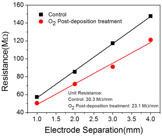
The resistance of the film of spiro-MeOTAD across the electrodes with and without O2 post-deposition treatments.
The photovoltaic parameters of CH3NH3PbI3-based devices with different post-deposition treatments are summarized in Table 1 while the I-V curves of the representative devices, which are close to the average performance for each post-deposition condition, are presented in Fig. 6a. The experimental data demonstrates substantial enhancement in the PCE (from 6.0% to 8.5%) for the ART-devices compared to the control devices (NRT-devices). The device performances were further improved when the samples were annealed in O2 at an elevated temperature. Under the optimized temperature (65°C), the JSC and fill factor of the A65-devices are significantly enhanced, yielding an average PCE of 12.0%. Since there is no obvious change in surface morphology and absorption as observed from SEM (Fig. S1) and absorption measurement (Fig. 1b) before and after O2 annealing process, the improvement in device performance is believed to originate from the lowering of the defect densities of the perovskite films. It is believed that the thermal annealing process may facilitate the diffusion of O2 to the perovskite film as well as the material interfaces to passivate the under-coordinated cations of the perovskite layer leading to the reduction in the density of the trap states and thereby reducing the recombination rate, which is reflected by the trend of obtained JSC shown in Fig. 6a. It is found that the JSC of the devices strongly depends on the post-deposition treatments, which is observed to increase from an average of 11.7 mA/cm2 for NRT-devices to 21.0 mA/cm2 for A65-devices, suggesting that charges can be extracted more efficiently, likely due to the inhibition of charge recombination at the trap states. Similar work for passivation of halide anions resulting in improved device performance has also been reported previously45. However, further increasing the thermal annealing temperature to 85°C resulted in a drop in the JSC, fill factor and accordingly PCE, which is possibly due to thermally induced degradation of the materials. Besides, a decrease in the magnitude of the JSC for the NRT-devices for V < 0.3 V is observed, which could be attributed to the low conductivity of spiro-MeOTAD and high density of interface states in the absence of O2 annealing, resulting in poor charge collection efficiency. It should be noted that hysteresis effect is generally observed in the I-V characteristics of all our devices, which basically remains unchanged even after the O2 annealing process. This suggests that the O2 annealing process is not able to eliminate the processes/defects responsible for the observed hysteresis effect. The I-V curves shown in the figures were obtained from the reverse scan at the scan rate of 0.01 V/s from 1.2 V to −0.2 V.
Table 1. The average values of photovoltaic parameters obtained from I-V measurements for planar CH3NH3PbI3 based solar cells with different post-deposition treatments and integrated photocurrent from the EQE spectra are indicated in the bracket.
| Type | VOC (V) | JSC (mA/cm2) | FF | η (%) | Δη (%) |
|---|---|---|---|---|---|
| NRT | 0.96 ± 0.02 | 11.7 ± 4.0 (10.6) | 0.48 ± 0.20 | 6.0 ± 3.7 | - |
| ART | 0.90 ± 0.12 | 19.5 ± 1.2 (15.3) | 0.48 ± 0.09 | 8.5 ± 2.6 | 42 |
| A45 | 0.99 ± 0.03 | 19.3 ± 0.4 (15.6) | 0.48 ± 0.03 | 9.2 ± 0.9 | 53 |
| A65 | 0.98 ± 0.01 | 21.0 ± 0.5 (20.5) | 0.57 ± 0.03 | 12.0 ± 0.7 | 100 |
| A85 | 0.97 ± 0.02 | 17.9± 2.6 (14.0) | 0.49 ± 0.02 | 8.6 ± 1.0 | 43 |
Figure 6.
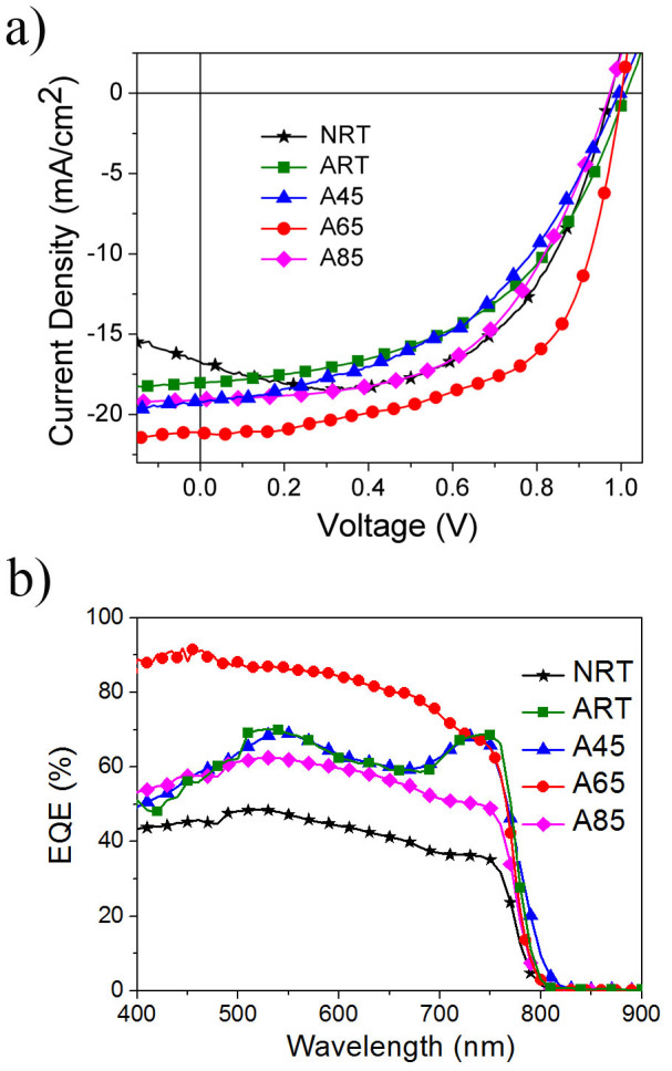
(a) The I-V curves and (b) EQE for representative devices with different post-deposition treatments.
The EQE spectra of CH3NH3PbI3-based devices with different post-deposition treatments are shown in Fig. 6b, which demonstrate wide spectral response from 400 nm to 800 nm in good agreement with the absorption spectra shown in Fig. 1b. The trend of the EQE spectra is also consistent with the I-V performance of the devices. There is a significant enhancement in EQE for the ART and A45 devices compared to the NRT devices. The EQE is further enhanced for the samples annealed in dry O2 at 65 °C while further increasing the annealing temperature to 85°C in the presence of O2 results in a reduction in the EQE. It is interesting to point out that a drop in the EQE results in the short wavelength range is typically attributed to high concentration of defect states in the front heterojunction. Detailed comparison between the EQE data for the control device (NRT) and the annealed device under optimal conditions (A65) we observe significant improvement in the EQE results at the short wavelength range. In general, the reduction in the EQE of solar cells can be attributed to charge recombination and short charge carrier diffusion length46, unequal enhancement in EQE along the spectrum is likely to occur when the condition of post-deposition treatment has not been completely optimized and considerable amount of traps still exist. It appears that O2 annealing may lead to an improvement in the carrier collection efficiency across the TiO2/perovskite interface47and the grain boundaries within the perovskite layer.
Detailed characterization of the time-resolved photoluminescence signal has been performed for both the control sample and the perovskite film annealed in O2 ambient at 65°C. The films were deposited directly on quartz substrates in order to pinpoint the effects of the O2 annealing process on the perovskite film. The experimental data are shown in Fig. 7. It is clear from the data that two separate lifetimes exist in the annihilation of the PL signal indicative of the presence of two recombination pathways48. Substantial improvements in the carrier lifetimes are observed in the O2 annealed sample indicating significant reduction in the density of the localized states in the perovskite film, which is consistent with the results of device performance. It is likely that most of these localized states reside at the grain boundaries however based on the data alone it is not possible to identify the specific location of the trap states. Further work needs to be done to specifically identify the mechanism underlying the observed phenomenon.
Figure 7.
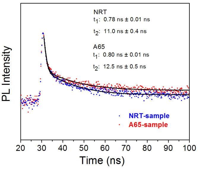
The time-resolved photoluminescence of the bare perovskite film with or without O2 post-deposition treatment.
By adopting the strategy of thermally assisted O2 annealing of the deposited films, a champion device with a PCE as high as 15.4% and a high JSC of 23 mA/cm2 can be achieved and the corresponding I-V curves are shown in Fig. 8. It is noted that the reproducibility of the perovskite-based solar cells can be significantly improved by post-deposition treatments, which is reflected by the lower values in the standard deviations in the photovoltaic parameters indicated in Table 1. The proposed fabrication strategy is straightforward and controllable for assembling highly efficient and good reproducible perovskite-based solar cells.
Figure 8.
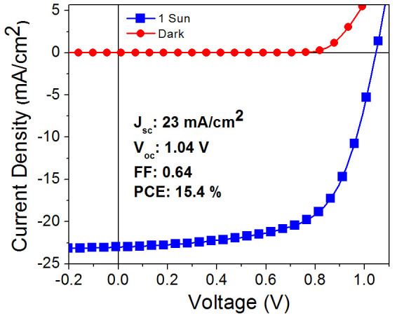
(a) The I-V curve of the best device measured at 100 mW/cm2 and in dark.
Discussion
CH3NH3PbI3-based devices have been fabricated under well controlled fabrication procedures. Our work demonstrated that post-deposition O2 treatments are critical, which not only enhance the device performance substantially, but also improve the device reproducibility. We found that placing the solution-processed films in dry O2 at 65°C prior to electrode deposition is an essential process for device fabrication, yielding an averaged enhanced PCE of 12%. Our results suggest that the improvement in device performance by O2 annealing process is due to the enhancement in the conductivity of spiro-MeOTAD as well as the reduction in the defect density of the perovskite film.
Methods
Materials
Patterned FTO coated glass substrates with a sheet resistance of 7-10 Ω/□ were supplied from KINTEC company. Lead (II) iodide (purity 99%, PbI2), titanium (IV) isopropoxide (TTIP), lithium bis(trifluoromethylsulphonyl)imide (Li-TFSI), 4-tert-butylpyridine (tBP), N,N-dimethylformamide (DMF) and MoO3 were purchased from Sigma-Aldrich while spiro-MeOTAD (purity> 99.5%) was purchased from Luminescence Technology Corp. Methylammonium iodide (CH3NH3I) was purchased from Dyenamo. All chemicals were used as received.
Device fabrication
Patterned FTO on glass substrates were cleaned sequentially by ultrasonication in toluene, acetone, ethanol and deionized water. The substrates were dried by the nitrogen flow and then exposed to UV-ozone for 20 min prior to the spin coating step. TiO2 compact layer was prepared by spin coating a mildly acidic diluted TTIP solution (1.25 ml) in ethanol (25 ml) at 3000 rpm followed by sintering at 450°C for 2 hours. CH3NH3PbI3 was synthesized by a two-step technique14 with optimized solution concentrations in N2 filled glove box. PbI2 films were prepared by spin coating a solution of PbI2 (1500 rpm) dissolved in DMF with a concentration of 462 mg/ml which were then annealed on a hotplate at 70°C for 1 hour prior to the reaction with CH3NH3I (30 mg/ml in isopropanol). The samples were then annealed at 90°C to ensure complete reaction between PbI2 and CH3NH3I. The hole transport layer (HTL) was prepared by spin coating a solution of spiro-MeOTAD (80 mg/ml) dissolved in chlorobenzene with the additives of Li-TFSI (17.5 µL from a stock solution of 520 mg/ml in acetonitrile) and 29 µL of tBP at 4500 rpm. The prepared samples were then stored in N2 ambient at room temperature or in O2 (high purity grade >99.9%) ambient at a flow rate of 2 lit/min at room temperature, 45°C, 65°C or 85°C for 12 hours. Electrodes (MoO3 (15 nm)/Al (120 nm)) were then deposited by thermal evaporation through a shadow mask and the device area was 0.1 cm2.
Device and sample characterizations
The I-V characteristics of the devices were measured using a B1500 A semiconductor parameter analyzer under the calibrated ABET Technologies SUN 2000 solar simulator equipped with an AM 1.5 filter at 100 mW/cm2. The I-V curves are obtained from the reverse scan at the scan rate of 0.01 Vs−1 from 1.2 V to −0.2 V. External quantum efficiency (EQE) was determined by a QE system from Enli Technology Co. Ltd. The surface morphologies of the films were characterized by atomic force microscopy (AFM) in the tapping mode using a Bruker NanoScope 8. UV-visible spectroscopy was performed by using a UV-2550 Shimadzu UV-VIS spectrophotometer for the perovskite film deposited on quartz. X-ray diffraction (XRD) patterns was determined by using a Rigaku SmartLab X-ray diffractometer in a step of 0.01° for 2θ from 10° to 70°. Scanning electron microscopy (SEM) was performed by using Hitachi S-4800 field emission scanning electron microscope. Time-resolved photoluminescence signals of perovskite film were monitored at 775 nm and recorded by using Edinburgh FLSP920 spectrophotometer equipped with the excitation source of 485 nm picosecond pulsed diode laser.
Author Contributions
C.S. proposed and supervised the whole project. Z.R. contributed to the device fabrication and process optimization for the entire project. A.B.D., W.W.-F.L. and W.K.C. involved the discussion of the experiments. Q.S. and A.N. assisted the preparation of experiments. J.W. and L.Y. prepared the solution of TiO2. Q.S. carried out the XRD and spiro-MeOTAD resistance measurement. H.C.G. performed the characterization of prepared films by AFM. Y.W.-K. examined the film morphology by SEM. J.H. and G.B. conducted the measurement of time-resolved photoluminescence. A.N. carried out the EQE measurement and wrote the manuscript.
Supplementary Material
Thermal Assisted Oxygen Annealing for High Efficiency Planar CH3NH3PbI3 Perovskite Solar Cells
Acknowledgments
This work was supported by the RGC Theme-based Research Scheme (Grant number: HKU T23-713/11).
References
- Kim H.-S., Im S. H. & Park N.-G. Organolead halide perovskite: New horizons in solar cell research. J. Phys. Chem. C 118, 5615–5625 (2014). [Google Scholar]
- Boix P. P., Nonomura K., Mathews N. & Mhaisalkar S. G. Current progress and future perspectives for organic/inorganic perovskite solar cells. Mater. Today 17, 16–23 (2014). [Google Scholar]
- Snaith H. J. Perovskites: The emergence of a new era for low-cost, high efficiency solar cells. J. Phys. Chem. Lett. 4, 3623–3630 (2013). [Google Scholar]
- Eperon G. E. et al. Formamidinium lead trihalide: a broadly tunable perovskite for efficient planar heterojunction solar cells. Energy Environ. Sci. 7, 982–988 (2014). [Google Scholar]
- Im J.-H., Lee C.-R., Lee J.-W., Park S.-W. & Park N.-G. 6.5% efficient perovskite quantum-dot-sensitized solar cell. Nanoscale 3, 4088–4093 (2011). [DOI] [PubMed] [Google Scholar]
- Stranks S. D. et al. Electron-hole diffusion lengths exceeding 1 micrometer in an organometal trihalide perovskite absorber. Science 342, 341–344 (2013). [DOI] [PubMed] [Google Scholar]
- Xing G. et al. Long-range balanced electron- and hole-transport lengths in organic-inorganic CH3NH3PbI3. Science 342, 344–347 (2013). [DOI] [PubMed] [Google Scholar]
- Lee M. M., Teuscher J., Miyasaka T., Murakami T. N. & Snaith H. J. Efficient hybrid solar cells based on meso-superstructured organometal halide perovskites. Science 338, 643–647 (2012) [DOI] [PubMed] [Google Scholar]
- Stoumpos C. C., Malliakas C. D. & Kanatzidis M. G. Semiconducting tin and lead iodide perovskites with organic cations: Phase transitions, high mobilities, and near-infrared photoluminescent properties. Inorg. Chem. 52, 9019–9038 (2013). [DOI] [PubMed] [Google Scholar]
- Hodes G. Perovskite-based solar cells. Science 342, 317–318 (2013). [DOI] [PubMed] [Google Scholar]
- Mitzi D. B. Synthesis, Structure, and Properties of Organic-Inorganic Perovskites and Related Materials. Prog. Inorg. Chem. 48, 1–121 (2007). [Google Scholar]
- Kojima A., Teshima K., Shirai Y. & Miyasaka T. Organometal halide perovskites as visible-light sensitizers for photovoltaics cells. J. Am. Chem. Soc. 131, 6050–6051 (2009). [DOI] [PubMed] [Google Scholar]
- Liu M., Johnston M. B. & Snaith H. J. Efficient planar heterojunction perovskite solar cells by vapour deposition. Nature 501, 395–398 (2013). [DOI] [PubMed] [Google Scholar]
- Burschka J. et al. Sequential deposition as a route to high-performance perovskite-sensitized solar cells. Nature 499, 316–319 (2013). [DOI] [PubMed] [Google Scholar]
- Jeon N. J. et al. Solvent engineering for high-performance inorganic-organic hybrid perovskite solar cells. Nat. Mater. 13, 897–903 (2014). [DOI] [PubMed] [Google Scholar]
- Zhou H. et al. Interface engineering of highly efficient perovskite solar cells. Science 345, 542–546 (2014). [DOI] [PubMed] [Google Scholar]
- Chen Q. et al. Planar heterojunction perovskite solar cell via vapor-assisted solution process. J. Am. Chem. Soc. 136, 622–625 (2014). [DOI] [PubMed] [Google Scholar]
- Kim H.-S. et al. Lead iodide perovskite sensitized all-solid-state submicron thin film mesoscopic solar cells with efficiency exceeding 9%. Sci. Rep. 2, 591; 10.1038/srep00591 (2012). [DOI] [PMC free article] [PubMed] [Google Scholar]
- Bi D. et al. Using a two-step deposition technique to prepare perovskite (CH3NH3PbI3) for thin film solar cells based on ZrO2 and TiO2 mesostructures. RCS Adv. 3, 18762–18766 (2013). [Google Scholar]
- Heo J. H. et al. Efficient inorganic-organic hybrid heterojunction solar cells containing perovskite compound and polymeric hole conductor. Nat. Photonics 7, 486–491 (2013). [Google Scholar]
- Christians J. A., Fung R. C. M. & Kamat P. V. An inorganic hole conductor for organo-lead halide perovskite solar cells. Improved hole conductivity with copper iodide. J. Am. Chem. Soc. 136, 758–764 (2014). [DOI] [PubMed] [Google Scholar]
- Kim H.-S. et al. High efficiency solid-state sensitized solar cell-based on submicrometer rutile TiO2 nanorod and CH3NH3PbI3 perovskite sensitizer. Nano Lett. 13, 2412–2417 (2013). [DOI] [PubMed] [Google Scholar]
- Dharani S. et al. High efficiency electrospun TiO2 nanofiber based hybrid organic-inorganic perovskite solar cell. Nanoscale 6, 1675–1679 (2014). [DOI] [PubMed] [Google Scholar]
- Son D.-Y., Im J.-H., Kim H.-S. & Park N.-G. 11% Efficient perovskite solar cell based on ZnO nanorods: an effective charge collection system. J. Phys. Chem. C 118, 16567–16573 (2014). [Google Scholar]
- Bi D. et al. Efficient and stable CH3NH3PbI3-sensitized ZnO nanorods array solid-state solar cells. Nanoscale 5, 11686–11691 (2013). [DOI] [PubMed] [Google Scholar]
- Kumar M. H. et al. Flexible, low-temperature, solution processed ZnO-based perovskite solid state solar cells. Chem. Commun. 49, 11089–11091 (2013). [DOI] [PubMed] [Google Scholar]
- Ball J. M., Lee M. M., Hey A. & Snaith H. J. Low-temperature processed meso-superstructured to thin-film perovskite solar cells. Energy Environ. Sci. 6, 1739–1743 (2013). [Google Scholar]
- Malinkiewicz O. et al. Perovskite solar cells employing organic charge- transport layers. Nat. Photonics 8, 128–132 (2014). [Google Scholar]
- Liu D. & Kelly T. L. Perovskite solar cells with a planar heterojunction structure prepared using room-temperature solution processing techniques. Nat. Photonics 8, 133–138 (2014). [Google Scholar]
- Liang P.-W. et al. Additive enhanced crystallization of solution-processed perovskite for highly efficient planar-heterojunction solar cells. Adv. Mater. 26, 3748–3754 (2014). [DOI] [PubMed] [Google Scholar]
- Jeng J.-Y. et al. CH3NH3PbI3 perovskite/fullerene planar-heterojunction hybrid solar cells. Adv. Mater. 25, 3727–3732 (2013). [DOI] [PubMed] [Google Scholar]
- Saliba M. et al. Influence of thermal processing protocol upon the crystallization and photovoltaic performance of organic-inorganic lead trihalide perovskites. J. Phys. Chem. C 118, 17171–17177 (2014). [Google Scholar]
- Conings B. et al. Perovskite-based hybrid solar cells exceeding 10% efficiency with high reproducibility using a thin films sandwich approach. Adv. Mater. 26, 2041–2046 (2014). [DOI] [PubMed] [Google Scholar]
- Eperon G. E., Burlakov V. M., Docampo P., Goriely A. & Snaith H. J. Morphological control for high performance solution-processed planar heterojunction perovskite solar cells. Adv. Funct. Mater. 24, 151–157 (2014). [Google Scholar]
- Wolf S. D. et al. Organometallic halide perovskite: Sharp Optical Absorption Edge and its relation to photovoltaic performance. J. Phys. Chem. Lett. 5, 1035–1039 (2014) [DOI] [PubMed] [Google Scholar]
- Mohammed I. M., Elbadawi A. A. & Abuellhassan H. H. Temperature and grain size effect on the electrical conductivity of La0.67Ca0.33MnO3. Journal of Applied and Industrial Sciences 1, 12–22 (2013). [Google Scholar]
- Baikie T. et al. Synthesis and crystal chemistry of the hybrid perovskite (CH3NH3)PbI3 for solid-state sensitised solar cell applications. J. Mater. Chem. A 1, 5628–5641 (2013). [Google Scholar]
- Sun S. et al. The origin of high efficiency in low-temperature solution-processable bilayer organometal halide hybrid solar cells. Energy Environ. Sci. 7, 399–407 (2014). [Google Scholar]
- Noh J. H., Im S. H., Heo J. H., Mandal T. N. & Seok S. I. Chemical Management for colorful, efficient, and stable inorganic−organic hybrid nanostructured solar cells. Nano Lett. 13, 1764–1769 (2013). [DOI] [PubMed] [Google Scholar]
- Abate A. et al. Lithium salts as “redox active” p-type dopants for organic semiconductor and their impact in solid-state dye-sensitized solar cells. Phys. Chem. Chem. Phys. 15, 2572–2579 (2013). [DOI] [PubMed] [Google Scholar]
- Ono L. K. et al. Air-exposure-induced gas molecule incorporation into spiro-MeOTAD films. J. Phys. Chem. Lett. 5, 1374–1379 (2014). [DOI] [PubMed] [Google Scholar]
- Cappel U. B., Daeneke T. & Bath U. Oxygen-induced doping of spiro-MeOTAD in solid-state dye-sensitized solar cells and its impact on device performance. Nano Lett. 12, 4925–4931 (2012). [DOI] [PubMed] [Google Scholar]
- So F. & Kondakov D. Degradation mechanisms in small-molecule and polymer organic light-emitting diodes. Adv. Mater. 22, 3762–3777 (2010). [DOI] [PubMed] [Google Scholar]
- Hermenau M. et al. Water and oxygen induced degradation of small molecule organic solar cells. Sol. Energy Mater. & Sol. Cells 95, 1268–1277 (2011). [Google Scholar]
- Abate A. et al. Supramolecular halogen bond passivation of organic-inorganic halide perovskite solar cells. Nano Lett. 14, 3247–3254 (2014). [DOI] [PubMed] [Google Scholar]
- Barkhouse D. A. R., Pattantyus-Abraham A. G., Levina L. & Sargent E. H. Thiols passivate recombination centers in colloidal quantum dots leading to enhanced photovoltaic device efficiency. ACS Nano 2, 2356–2362 (2008). [DOI] [PubMed] [Google Scholar]
- Lira-Cantu M., Norrman K., Andreasen J. W. & Krebs F. C. Oxygen release and exchange in niobium oxide MEHPPV hybrid solar cells. Chem. Mater. 18, 5684–5690 (2006). [Google Scholar]
- Chen Q. et al. Controllable self-induced passivation of hybrid lead iodide perovskites toward high performance solar cells. Nano Lett. 14, 4158–4163 (2014). [DOI] [PubMed] [Google Scholar]
Associated Data
This section collects any data citations, data availability statements, or supplementary materials included in this article.
Supplementary Materials
Thermal Assisted Oxygen Annealing for High Efficiency Planar CH3NH3PbI3 Perovskite Solar Cells


