Abstract

Transition metal dichacogenides represent a unique class of two-dimensional layered materials that can be exfoliated into single or few atomic layers. Tungsten diselenide (WSe2) is one typical example with p-type semiconductor characteristics. Bulk WSe2 has an indirect band gap (∼1.2 eV), which transits into a direct band gap (∼1.65 eV) in monolayers. Monolayer WSe2, therefore, is of considerable interest as a new electronic material for functional electronics and optoelectronics. However, the controllable synthesis of large-area WSe2 atomic layers remains a challenge. The studies on WSe2 are largely limited by relatively small lateral size of exfoliated flakes and poor yield, which has significantly restricted the large-scale applications of the WSe2 atomic layers. Here, we report a systematic study of chemical vapor deposition approach for large area growth of atomically thin WSe2 film with the lateral dimensions up to ∼1 cm2. Microphotoluminescence mapping indicates distinct layer dependent efficiency. The monolayer area exhibits much stronger light emission than bilayer or multilayers, consistent with the expected transition to direct band gap in the monolayer limit. The transmission electron microscopy studies demonstrate excellent crystalline quality of the atomically thin WSe2. Electrical transport studies further show that the p-type WSe2 field-effect transistors exhibit excellent electronic characteristics with effective hole carrier mobility up to 100 cm2 V–1 s–1 for monolayer and up to 350 cm2 V–1 s–1 for few-layer materials at room temperature, comparable or well above that of previously reported mobility values for the synthetic WSe2 and comparable to the best exfoliated materials.
Keywords: layered materials, semiconductor, tungsten diselenide, field effect transistor, large area growth
Graphene has attracted considerable interest for applications in diverse electronic and optoelectronic devices due to its unique electronic properties and atomically thin geometry.1−12 However, the gapless band structure limits the potential of graphene for digital electronic devices.2,4 It has been shown the energy band structure of the transition metal dichalcogendes (TMD) materials exhibit a unique indirect-to-direct band gap transition as their layer number is reduced to one.13−18 For example, bulk WSe2 is a p-type semiconductor with an indirect band gap of ∼1.2 eV, whereas its monolayer exhibits a direct band gap of ∼1.65 eV.17,19 The direct band gap of atomically thin TMDs can offer exciting opportunities for potential applications in both digital electronic and optoelectronic devices.20−24 For example, it has been recently reported that exfoliated monolayer WSe2 can be used to create a high performance p-type field-effect transistor (FET).25 However, the size of the monolayer materials obtained from mechanical exfoliation method is limited in a few to a few tens of micrometers. It has also been recently reported that a chemical vapor deposition approach can be used to grow WSe2 atomic flakes, but only in separated domains with the domain size on the order of 10 μm.26−28 Therefore, the preparation of large-area monolayer WSe2 film is essential for practical applications yet remains a significant challenge.
Here, we report a systematic study of chemical vapor deposition approach for the preparation of large area atomically thin WSe2 films directly on SiO2/Si substrates with areal size of monolayer WSe2 film up to 1 cm2. Microphotoluminescence mapping demonstrates distinct layer-number dependent photoluminescence, with the monolayer area exhibit much stronger emission than bilayer or multilayers. The transmission electron microscopy (TEM) studies reveal excellent crystalline quality of the atomically thin WSe2 and electrical transport studies further demonstrate that the p-type WSe2 field-effect transistors exhibit excellent electronic characteristics with hole carrier mobility up to 100 cm2 V–1 s–1 for monolayer and up to 350 cm2 V–1 s–1 for few-layer materials, comparable or well above that of previously reported mobility values or the synthetic WSe2 and comparable to the best exfoliated materials.26,29−31
The growth processes are performed in a homemade tube furnace with detailed growth procedures described in the Experimental section in Supporting Information. Briefly, the WSe2 powders are placed in an alumina boat at the center of a quartz tube inside a one-inch tube furnace, and the clean SiO2/Si substrates are used as the growth substrate for the deposition of WSe2 atomic layers at the downstream end with variable substrate temperature. Argon is continuously supplied through the reactor with designed flow rate as the carrier gas. We have first conducted systematic studies to investigate the effect of substrate temperature and flow rate of carrier gas with a constant source temperature at 1060 °C (Figure 1). Most of the WSe2 domains exhibit a triangular shape as shown by the optical microscope images in Figure 1b, c and Figure 2a–c, and some of them show a hexagonal shape as shown in Figure 1d, g, and l. In general, with a fixed source temperature, the lower substrate temperature typically results in a higher nucleation density, and a higher flow rate of the carrier gas produces a similar effect due to higher supersaturation of the precursors over the substrate surface. On the other hand, the higher substrate temperature promotes the nucleation of the extra atomic layers to produce multilayers.
Figure 1.
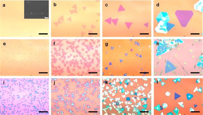
Reactor-conditions-dependent WSe2 growth with varying temperature and flow rate of argon. Optical microscope images of WSe2 samples grown at different temperature under designed flow rate for 20 min: (a) 750 °C, 100 sccm (inset: SEM image of same size sample, indicating high density but small nucleations (∼300 to 500 nm); scale bar, 5um); (b) 765 °C, 100 sccm; (c) 780 °C, 100 sccm; (d) 795 °C, 100 sccm; (e) 750 °C, 150 sccm; (f) 765 °C, 150 sccm; (g) 780 °C, 150 sccm; (h) 795 °C, 150 sccm; (i) 750 °C, 200 sccm; (j) 765 °C, 200 sccm; (k) 780 °C, 200 sccm; (l) 795 °C, 200 sccm. All of the scale bars are 20 μm.
Figure 2.
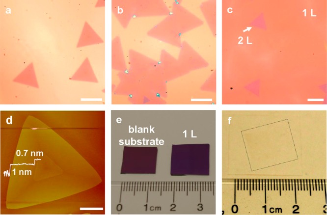
Time dependent growth of large area monolayer WSe2 single crystal domains. (a) Typical optical microscope images of the monolayer WSe2 domains taken after 20 min of growth, (b) 30 min of growth, and (c) 40 min of growth. (d) Atomic force microscope image of a WSe2 monolayer and bilayer domains and their line scan profile. (e) Photograph of the ∼1 cm sized monolayer WSe2 films obtained with 40 min growth time. Left: blank 300 nm SiO2/Si substrate. Right: fully covered WSe2 monolayer on blank 300 nm SiO2/Si substrate. (f) Photograph of the ∼1 cm sized monolayer WSe2 films transferred onto a glass template by chemical etching of SiO2 layers. Scale bars of panels a–d are all 5 μm.
At lower substrate temperature of 750 °C with low flow rate of 100 sccm, there are no visible WSe2 domains observed on the SiO2/Si substrates under optical microscope. However, after analyzing the same sample by using scanning electron miscroscopy (SEM), very small nucleations (∼300 nm of average edge size) were observed with nucleation density of ∼4200/mm2. By increasing the substrate temperature to 765 °C, the monolayer WSe2 domains (∼10 μm of average edge size) start to appear with a nucleation density of ∼1060/mm2 (Figure 1b). When the growth temperature reaches 780 °C, the bilayer WSe2 domains (∼20 μm of average edge size) start to appear with an overall lower domain density reduced to ∼350/mm2 (Figure 1c). As the growth temperature is further increased to 795 °C, even thicker and larger flakes (∼50 μm of average edge size) appear with even lower domain density of ∼280/mm2 (Figure 1d). Overall, higher growth temperature yields a lower density of thicker WSe2 domains with a larger domain size. By increasing the flow rate of the carrier gas, both the layer number and the domain density of the WSe2 are increased. For instance, at growth temperature of 765 °C, the nucleation density is ∼1060/mm2 under 100 sccm flow rate of carrier gas, which increases to ∼11 000/mm2 under 150 sccm, and ∼23 000/mm2 under 200 sccm. All of our observations are consistent with the nucleation model of the vapor phase deposition developed by W. K. Burton and N. Cabrera, where they predict that the nucleation probability is proportional to the supersaturation and inversely proportional to the substrate temperature.32
Based on the above studies, we have identified an optimized condition for the large area growth of WSe2 monolayers at a substrate temperature of 765 °C and 100 sccm of carrier gas. Figure 2a shows the OM images of typical triangular WSe2 monolayers after 20 min growth with an average edge length of approximately 5 μm. With the continued growth, the monolayer domains starts to merge together at 30 min, with bilayer and few-layer domains occasionally appeared on their first layer (Figure 2b). After 40 min growth, the WSe2 monolayer domains are completely merged together to form a continuous monolayer, with a few second layer triangular domains seen with different optical contrast (Figure 2c). In this case, the SiO2/Si substrates are completely covered by the monolayer WSe2 domains with less than 5% areal coverage of the bilayer. The number of WSe2 atomic layers is also determined by AFM measurements (Figure 2d). The AFM step height of WSe2 monolayer on the SiO2 substrate is typically measured between 0.7–1.0 nm, and the step heights of the second layer on monolayer is around ∼0.7 nm (line scan in Figure 2d), which is consistent with the published reports of exfoliated WSe2.14,15 The larger step height observed in the first layer is commonly seen in graphene or other layered materials such as MoSe2.16 The lateral size of the resulted continuous monolayer WSe2 film is as large as 1 cm2 and is only limited by the size of the furnace (Figure 2e). The large area monolayer WSe2 film can be readily transferred onto another substrate such as the glass (Figure 2f). We have further investigated the layer number dependent morphological and optical properties of the resulting atomically thin WSe2 films. To this end, we have employed the μ-Raman to study the monolayer/bilayer WSe2 domains. The bilayer WSe2 domain shows a triangular shape, which prefers to crystallize from the center of the first layer. The layer number of the WSe2 domains is further confirmed using μ-Raman studies. The Raman spectrum of monolayer region shows a single peak at 252 cm–1 (green line in Figure 3b), corresponding to the A1g resonance mode of WSe2; and that of bilayer area shows an additional small peak at 307 cm–1 (red line in Figure 3b), corresponding to the B2g resonance mode of WSe2. In general, the B2g signature mode is only active on the bilayer or few-layer region, which could reflect the presence of the additional interlayer interaction.14,15 In contrast, the Raman A1g mode of WSe2 is less sensitive to layer thickness, only with the intensity increasing with reducing atomic layers. The corresponding Raman map recorded at A1g mode can be further used to determine the layer number of the WSe2 (Figure 3c–f). The darker triangular region on the Raman map of A1g mode corresponds to the bilayer or few-layer WSe2 domain. The Raman mapping shows nearly the same color contrast throughout the monolayer and bilayer or few-layer area, indicating a uniform crystal quality.
Figure 3.
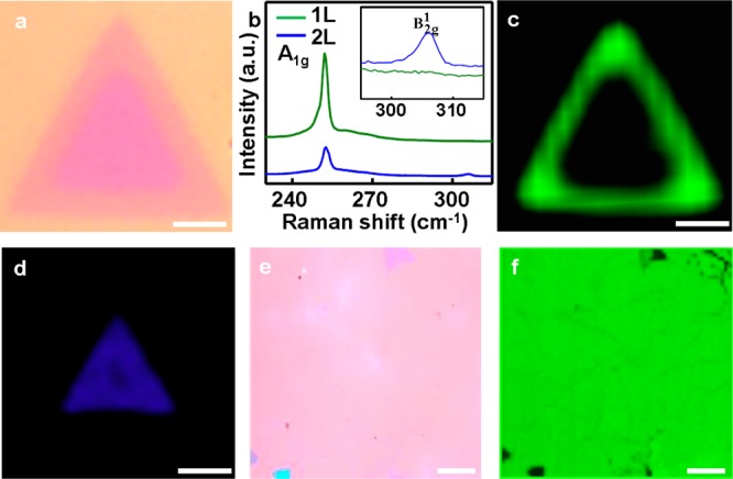
Micro-Raman investigation of the monodomain WSe2. (a) Optical microscope image of a typical monolayer WSe2 with bilayer domain on the center. (b) The Raman spectra of the monolayer and bilayer WSe2. (c) and (d) Typical Raman map of the single domain monolayer (c, center wavenumber: ∼ 252 cm–1) with bilayer (d, center wavenumber: ∼ 307 cm–1) WSe2 domain. (e) Optical microscope image of large scale monolayer WSe2 with several bilayer or few-layer domain. (f) Raman map of the large scale monolayer (center wavenumber: ∼ 250 cm–1) WSe2 with several bilayer and few-layer domain. Scale bars of panels a, c, and d are all 5 μm; Scale bars of panels e and f are 10 μm.
The optical properties of the monolayer WSe2 domains and the continuous WSe2 sheets were further investigated using microphotoluminescence (μ-PL). The WSe2 monodomain with single layer shows the PL peak located at approximately 767 nm, with full-width-half-maximum (FWHM) values of 25 nm (Figure 4b), which is comparable to the published data for exfoliated WSe2.14,15 The corresponding μ-PL map of the monolayer WSe2 single crystal domain shows a very uniform contrast (Figure 4c), indicating the high crystalline quality and uniformity of the as-grown WSe2 atomic layers. We have also conducted μ-PL studies on the continuous WSe2 film that are merged together (Figure 4d). The μ-PL spectra taken of the monolayer region show the characteristic peak around 766 nm (red curve in Figure 4e). The strong light emission from monolayer indicates the high quality of the continuous WSe2 films. The μ-PL spectra taken at bilayer WSe2 region (the darker triangular area on the OM image in Figure 4d) shows a wider peak at ∼790 nm with significantly lower intensity (black curve in Figure 4e). We have further conducted μ-PL mapping studies over a relatively large area (∼60 × 60 μm) to evaluate the overall quality of the material (Figure 4f). Importantly, the PL mapping shows rather uniform emission across the entire film, indicating that the film is largely consisted of monolayer crystals. There are a few darker triangles in the PL mapping image, corresponding to the bilayer region. Additionally, it is also noted that there are some slightly darker lines, which can be attributed to the grain boundaries between merged monolayer domains.
Figure 4.
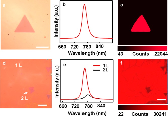
Optical properties of the single domain and fully covered WSe2 monolayers. (a) Optical microscope image of a typical monolayer WSe2. Scale bar is 5 μm. (b) PL spectra of the monolayer WSe2 and PL map (c) of WSe2 single domain showed in panel a. (d) Optical microscope image of the full covered monolayer WSe2 with some bilayer domains. Scale bar is 10 μm. (e) PL spectra of the monolayer and bilayer WSe2. (f) Corresponding PL map of the same region taken at panel d. Scale bar is 10 μm.
To further evaluate the atomic structure of the WSe2 atomic layers, we have performed high resolution transmission electron microscopy (HRTEM) and electron diffraction (ED) studies. To this end, the as-grown WSe2 crystals were transferred onto a carbon-coated TEM grid. Figure 5a is the optical microscopy image. Figure 5b shows a low magnification TEM image of a typical transferred WSe2 triangular crystal, which shows increasing contrast from the edge to the center, with three distinct regions corresponding to the monolayer, bilayer, and few-layer area. The energy dispersive X-ray studies demonstrate that the atomic ratio between W and Se is approximately 1:2 (Figure 5c), consistent with the expected stoichiometry. We have further conducted HRTEM on different regions of the same WSe2 flake. Figure 5d–f show the HRTEM images of the atomic structure of the WSe2 monolayer, bilayer, and multilayers, respectively. These images were taken on the regions indicated on Figure 5b by the arrows with blue, red, and dark cyan colors, respectively. The hexagonal lattice is clearly visible from each atomic resolution image, confirming the excellent crystalline quality of the atomic layered material. The selected-area electron diffraction (SAED) is used to characterize the crystal structure of the film. Figure 5g–i show the SAED patterns of the monolayer, bilayer, and few-layer WSe2 with the zone axis of [0001]. The single set of diffraction spots with 6-fold symmetry demonstrates that the triangular monolayer is single crystals with hexagonal structures.33,34
Figure 5.
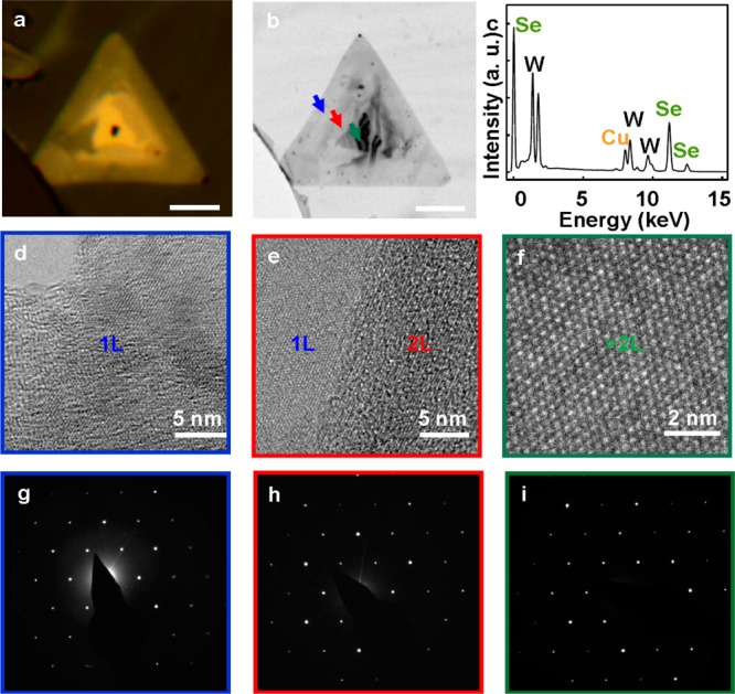
Crystalline structure characterization. (a) Optical microscope image of a typical monolayer WSe2 with domain of few layers on the center. Scale bar is 10 μm. (b) Low magnification bright field TEM image of a typical transferred WSe2 triangular crystal. (c) Energy dispersive X-ray spectra showing the ratio between W and Se obtained from the integrated peak area is approximately 1:2. (d–f) HRTEM images of the atomic structure of the WSe2 monolayer (d), bilayer (e), and multilayers. These images were taken on the regions indicated on panel b by the arrows with blue, red, and dark cyan colors, respectively. Scale bars are 5 nm (d,e) and 2 nm (f). (g–i) SAED pattern of the monolayer (g), bilayer (h) and few-layer (i) WSe2 with the zone axis of [0001], the 6-fold symmetry in the position of the diffraction spots demonstrates that the triangular monolayer is predominantly single crystal with hexagonal structures.
We have further evaluated the electronic properties of the WSe2 atomic layers. To this end, we have fabricated back-gated field-effect transistors (FETs) from the synthetic WSe2 on the 300 nm SiO2/Si substrates (Figure 6a). The source and drain electrodes (100 nm Au) defined by the electron beam lithography (EBL) and deposited using thermal evaporation. More than 100 transistors were fabricated on WSe2 monolayer, bilayer, and few-layer monodomains. The standard transistor measurements were conducted under ambient conditions to obtain the on-currents, carrier mobilities, and on/off ratios for all devices. Figure 6b shows the Ids–Vds output characteristic of a monolayer WSe2 FETs at various gate voltages. The linear and symmetric curves suggested that ohmic contacts were formed at the source and drain electrodes. The Ids–Vbg curve of the same device was measured at different drain bias from 0 to 4 V, with the back-gate voltage sweeping from −100 to 100 V (Figure 6c). Additionally, the Ids–Vbg curve of the typical WSe2 monolayer, bilayer and few-layer FETs are shown in Supporting Information Figure S2. All these IV curves show typical p-type semiconductor characteristic, consistent with mechanically exfoliated WSe2 materials. The highest mobility of the monolayer WSe2 FETs is 100 cm2 V–1 s–1. The measured on/off ratio of this device reaches a maximum value above 1 × 10⁸ for gate voltages swept in the range from −100 to 100 V with a source-drain bias of 2 V, which is comparable to the best reported values for exfoliated samples, and greatly higher than synthetic samples reported previously. After analysis of all the fabricated WSe2 FETs, we have plotted a histogram to show the mobility distribution for all devices (Figure 6d). Importantly, the highest mobility of the few-layer WSe2 FETs can reach up to 350 cm2 V–1 s–1, which represents the highest value observed in these atomically thin TMDs at room temperature,26,35−40 further highlighting the high crystalline quality of these as-grown materials.
Figure 6.
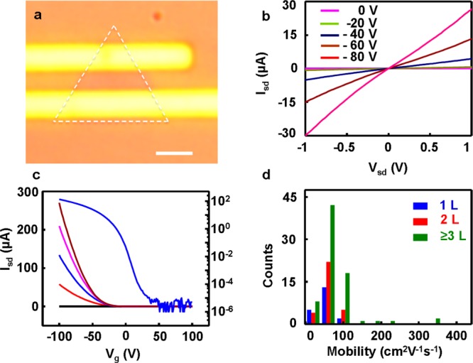
Electronic properties of WSe2 atomic layers. (a) Optical microscope image of a monolayer WSe2 transistor; scale bar is 2 μm. (b) Isd–Vsd output characteristics of the WSe2 transistor shown in panel a. (c) Isd–Vg transfer characteristics of the device shown in (a) at Vsd = 0, 1, 2, 3, and 4 V. (d) Summary of the mobility values obtained in WSe2 field effect transistors with different number of atomic layers, demonstrating a mobility range of 10–350 cm2 V–1 s–1 and maximum on/off ratio over 108.
In summary, we have reported a systematic investigation on the chemical vapor deposition growth of large area p-type WSe2 atomic layers. By systematically tuning the synthetic parameters, we show that high quality monolayer WSe2 thin film can be prepared over large area with the lateral dimensions up to ∼1 cm2. Microphotoluminescence studies demonstrate uniform PL emission from the monolayer materials and the transmission electron microscopy studies confirm the excellent crystalline quality. Electrical transport studies further demonstrate the p-type WSe2 back-gated field-effect transistors exhibit excellent electronic characteristics with hole mobility over 350 cm2 V–1 s–1 and on/off ratio above 108. The availability of high quality large area p-type atomically thin materials offers an important building block for the design of future van de Waals heterostructures for electronic and photonic devices.
Acknowledgments
We acknowledge the Nanoelectronics Research Facility (NRF) at UCLA for technical support. X.D. acknowledges support by NSF CAREER award 0956171. Y.H. acknowledges the NIH Director’s New Innovator Award Program 1DP2OD007279.
Supporting Information Available
Experimental details; Figures S1–S2. This material is available free of charge via the Internet at http://pubs.acs.org.
Author Contributions
∥ These authors contribute equally to this work
The authors declare no competing financial interest.
Funding Statement
National Institutes of Health, United States
Supplementary Material
References
- Novoselov K. S.; Fal’ko V. I.; Colombo L.; Gellert P. R.; Schwab M. G.; Kim K. Nature 2012, 4907419192–200. [DOI] [PubMed] [Google Scholar]
- Schwierz F. Nat. Nanotechnol. 2010, 57487–496. [DOI] [PubMed] [Google Scholar]
- Bonaccorso F.; Sun Z.; Hasan T.; Ferrari A. C. Nat. Photonics 2010, 49611–622. [Google Scholar]
- Weiss N. O.; Zhou H. L.; Liao L.; Liu Y.; Jiang S.; Huang Y.; Duan X. F. Adv. Mater. 2012, 24435782–5825. [DOI] [PMC free article] [PubMed] [Google Scholar]
- Liao L.; Lin Y. C.; Bao M. Q.; Cheng R.; Bai J. W.; Liu Y. A.; Qu Y. Q.; Wang K. L.; Huang Y.; Duan X. F. Nature 2010, 4677313305–308. [DOI] [PMC free article] [PubMed] [Google Scholar]
- Bao Q. L.; Loh K. P. ACS Nano 2012, 653677–3694. [DOI] [PubMed] [Google Scholar]
- Lin Y. M.; Valdes-Garcia A.; Han S. J.; Farmer D. B.; Meric I.; Sun Y. N.; Wu Y. Q.; Dimitrakopoulos C.; Grill A.; Avouris P.; Jenkins K. A. Science 2011, 33260351294–1297. [DOI] [PubMed] [Google Scholar]
- Britnell L.; Gorbachev R. V.; Jalil R.; Belle B. D.; Schedin F.; Mishchenko A.; Georgiou T.; Katsnelson M. I.; Eaves L.; Morozov S. V.; Peres N. M. R.; Leist J.; Geim A. K.; Novoselov K. S.; Ponomarenko L. A. Science 2012, 3356071947–950. [DOI] [PubMed] [Google Scholar]
- Yang H.; Heo J.; Park S.; Song H. J.; Seo D. H.; Byun K. E.; Kim P.; Yoo I.; Chung H. J.; Kim K. Science 2012, 33660851140–1143. [DOI] [PubMed] [Google Scholar]
- Xia F. N.; Mueller T.; Lin Y. M.; Valdes-Garcia A.; Avouris P. Nat. Nanotechnol. 2009, 412839–843. [DOI] [PubMed] [Google Scholar]
- Liu Y.; Cheng R.; Liao L.; Zhou H. L.; Bai J. W.; Liu G.; Liu L. X.; Huang Y.; Duan X. F. Nat. Commun. 2011, 2, 579. [DOI] [PMC free article] [PubMed] [Google Scholar]
- Mueller T.; Xia F. N. A.; Avouris P. Nat. Photonics 2010, 45297–301. [Google Scholar]
- Splendiani A.; Sun L.; Zhang Y. B.; Li T. S.; Kim J.; Chim C. Y.; Galli G.; Wang F. Nano Lett. 2010, 1041271–1275. [DOI] [PubMed] [Google Scholar]
- Li H.; Lu G.; Wang Y. L.; Yin Z. Y.; Cong C. X.; He Q. Y.; Wang L.; Ding F.; Yu T.; Zhang H. Small 2013, 9111974–1981. [DOI] [PubMed] [Google Scholar]
- Tonndorf P.; Schmidt R.; Bottger P.; Zhang X.; Borner J.; Liebig A.; Albrecht M.; Kloc C.; Gordan O.; Zahn D. R. T.; de Vasconcellos S. M.; Bratschitsch R. Opt. Express 2013, 2144908–4916. [DOI] [PubMed] [Google Scholar]
- Xu Y. X.; Huang X. Q.; Lin Z. Y.; Zhong X.; Huang Y.; Duan X. F. Nano Res. 2013, 6165–76. [Google Scholar]
- Terrones H.; Lopez-Urias F.; Terrones M. Sci. Rep. 2013, 3, 1549. [DOI] [PMC free article] [PubMed] [Google Scholar]
- Lee Y. H.; Yu L. L.; Wang H.; Fang W. J.; Ling X.; Shi Y. M.; Lin C. T.; Huang J. K.; Chang M. T.; Chang C. S.; Dresselhaus M.; Palacios T.; Li L. J.; Kong J. Nano Lett. 2013, 1341852–1857. [DOI] [PubMed] [Google Scholar]
- Kumar A.; Ahluwalia P. K.. Eur. Phys. J. B 2012, 85, (6).
- Najmaei S.; Liu Z.; Zhou W.; Zou X. L.; Shi G.; Lei S. D.; Yakobson B. I.; Idrobo J. C.; Ajayan P. M.; Lou J. Nat. Mater. 2013, 128754–759. [DOI] [PubMed] [Google Scholar]
- Wang Q. H.; Kalantar-Zadeh K.; Kis A.; Coleman J. N.; Strano M. S. Nat. Nanotechnol. 2012, 711699–712. [DOI] [PubMed] [Google Scholar]
- Yu W. J.; Liu Y.; Zhou H. L.; Yin A. X.; Li Z.; Huang Y.; Duan X. F. Nat. Nanotechnol. 2013, 812952–958. [DOI] [PMC free article] [PubMed] [Google Scholar]
- Yu W. J.; Li Z.; Zhou H. L.; Chen Y.; Wang Y.; Huang Y.; Duan X. F. Nat. Mater. 2013, 123246–252. [DOI] [PMC free article] [PubMed] [Google Scholar]
- Zhu C. F.; Zeng Z. Y.; Li H.; Li F.; Fan C. H.; Zhang H. J. Am. Chem. Soc. 2013, 135165998–6001. [DOI] [PubMed] [Google Scholar]
- Fang H.; Chuang S.; Chang T. C.; Takei K.; Takahashi T.; Javey A. Nano Lett. 2012, 1273788–3792. [DOI] [PubMed] [Google Scholar]
- Huang J. K.; Pu J.; Hsu C. L.; Chiu M. H.; Juang Z. Y.; Chang Y. H.; Chang W. H.; Iwasa Y.; Takenobu T.; Li L. J. ACS Nano 2014, 81923–930. [DOI] [PubMed] [Google Scholar]
- Cheng R.; Li D.; Zhou H.; Wang C.; Yin A.; Jiang S.; Liu Y.; Chen Y.; Huang Y.; Duan X. Nano Lett. 2014, 14105590–5597. [DOI] [PMC free article] [PubMed] [Google Scholar]
- Duan X.; Wang C.; Shaw J. C.; Cheng R.; Chen Y.; Li H.; Wu X.; Tang Y.; Zhang Q.; Pan A.; Jiang J.; Yu R.; Huang Y. Nat. Nanotechnol. 2014, 10.1038/nnano.2014.222. [DOI] [PubMed] [Google Scholar]
- Fang H.; Tosun M.; Seol G.; Chang T. C.; Takei K.; Guo J.; Javey A. Nano Lett. 2013, 1351991–1995. [DOI] [PubMed] [Google Scholar]
- Chuang H. J.; Tan X. B.; Ghimire N. J.; Perera M. M.; Chamlagain B.; Cheng M. M. C.; Yan J. Q.; Mandrus D.; Tomanek D.; Zhou Z. X. Nano Lett. 2014, 1463594–3601. [DOI] [PubMed] [Google Scholar]
- Liu W.; Kang J. H.; Sarkar D.; Khatami Y.; Jena D.; Banerjee K. Nano Lett. 2013, 1351983–1990. [DOI] [PubMed] [Google Scholar]
- Burton W. K.; Cabrera N. Discuss. Faraday Soc. 1949, 533–39. [Google Scholar]
- Liu L. X.; Zhou H. L.; Cheng R.; Yu W. J.; Liu Y.; Chen Y.; Shaw J.; Zhong X.; Huang Y.; Duan X. F. ACS Nano 2012, 698241–8249. [DOI] [PMC free article] [PubMed] [Google Scholar]
- Zhou H. L.; Yu W. J.; Liu L. X.; Cheng R.; Chen Y.; Huang X. Q.; Liu Y.; Wang Y.; Huang Y.; Duan X. F. Nat. Commun. 2013, 4, 10.1038/ncomms3096. [DOI] [PubMed] [Google Scholar]
- Liu L. T.; Kumar S. B.; Ouyang Y.; Guo J. IEEE Trans. Electron Devices 2011, 5893042–3047. [Google Scholar]
- Lee Y. H.; Zhang X. Q.; Zhang W. J.; Chang M. T.; Lin C. T.; Chang K. D.; Yu Y. C.; Wang J. T. W.; Chang C. S.; Li L. J.; Lin T. W. Adv. Mater. 2012, 24172320–2325. [DOI] [PubMed] [Google Scholar]
- Huang X.; Zeng Z. Y.; Zhang H. Chem. Soc. Rev. 2013, 4251934–1946. [DOI] [PubMed] [Google Scholar]
- Zhan Y. J.; Liu Z.; Najmaei S.; Ajayan P. M.; Lou J. Small 2012, 87966–971. [DOI] [PubMed] [Google Scholar]
- Liu K. K.; Zhang W. J.; Lee Y. H.; Lin Y. C.; Chang M. T.; Su C.; Chang C. S.; Li H.; Shi Y. M.; Zhang H.; Lai C. S.; Li L. J. Nano Lett. 2012, 1231538–1544. [DOI] [PubMed] [Google Scholar]
- Larentis S.; Fallahazad B.; Tutuc E. Appl. Phys. Lett. 2012, 10122223104. [Google Scholar]
Associated Data
This section collects any data citations, data availability statements, or supplementary materials included in this article.


