Abstract
Simultaneously optimizing electrical and thermal transport properties of bulk thermoelectric materials remains a key challenge due to the conflicting combination of material traits. Here, we have explored the electrical and thermal transport features of In-filled CoSb3 through X-ray absorption fine structure, X-ray photoemission spectra, transport measurement and theoretical calculation. The results provide evidence of three types of coexisting multi-localization transport behaviours in the material; these are heat-carrying phonon-localized resonant scattering, accelerated electron movement and increase in density of states near the Fermi level. The 5p-orbital hybridization between In and Sb is discovered in the In-filled CoSb3 compound, which results in a charge transfer from Sb to In and the enhancement of p–d orbital hybridization between Co and Sb. Our work demonstrates that the electrical and thermal properties of filled skutterudite bulk thermoelectric materials can be simultaneously optimized through the three types of coexisting multi-localization transport behaviours in an independent way.
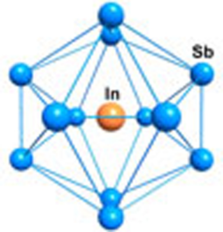 An ideal thermoelectric material has a large Seebeck coefficient, and a high electrical but low thermal conductivity; however, optimizing all three is difficult. Zhao et al. discover three types of coexisting multi-localization transport behaviours in filled skutterudite materials that aid this optimization.
Thermoelectric (TE) devices, which can directly convert heat into electricity and vice versa, have attracted considerable attention due to a variety of applications in heating, cooling, power generation and waste heat recovery1. Their conversion efficiency depends on the dimensionless figure of merit of TE materials defined as ZT=α2σT/κ, where T is the absolute temperature, σ is the electrical conductivity, α is the Seebeck coefficient and κ is the total thermal conductivity (κ=κE+κL, where κE is the electronic contribution and κL the lattice contribution). Numerous efforts have been attempted to improve ZT in the past two decades despite a compromise of κ and α with σ in TE materials2. To decrease κL, various approaches used to enhance phonon scattering have taken advantage of nanoinclusion3,4,5,6, alloying7, rattling filler8, quasi-ballistic transport nanoscale interfaces or nanopores9,10, liquid-like behaviour copper ions11 and anharmonic phonon coupling12. Meanwhile, a series of band structure engineering approaches such as high valley degeneracy13,14, peierls distortion15, electron energy filtering near the Fermi level16,17,18 and optimal bandwidth19, have been employed to improve the electrical properties. Some important single-localization transport behaviours have been discovered in different TE materials. For example, interface scattering in AgPbmSbTe2+m (ref. 4) and BiSbTe (ref. 6), and localized resonant scattering in filled CoSb3 (ref. 8) have remarkably enhanced phonon scattering and reduced κL; band convergence in PbTe1−xSex (ref. 13) and Mg2Si1−xSnx (ref. 14), charge density wave in In4Se3 (ref. 15) and electron resonant state in PbTe (ref. 16) have all led to an effective increase in α. These single-localization transport behaviour, however, can only optimize a single physical parameter of electrical or thermal properties. So far, it remains a major challenge to simultaneously increase α and σ while reducing κ, because no material has been found that shows multiple-localization transport behaviour.
Filled CoSb3 have been intensely pursued as an important TE material for intermediate-temperature power generation. The major progress in improving ZT has made through decreasing κL by filling the icosahedron voids in CoSb3 with foreign atoms (for example, rare earths, alkali earths or alkali metals) to enhance heat-carrying phonon-localized resonant scattering via filler rattling8,20,21,22,23,24,25,26,27,28,29. Shi et al.28 suggested that the electrical properties of multiple-filled CoSb3 could be optimized by adjusting the total filling fraction of fillers with different charge states. However, the tuning space of electrical properties is limited due to the conflicting relationship among α, n and σ, as expressed in the following formulae:
 |
 |
where m* is the carrier effective mass; n, the carrier concentration and μH, the carrier mobility. Recently, more and more experiments indicate that group III elements (Ga, In and Tl) can remarkably improve ZT of CoSb3 materials because of an almost perfect combination of low κL, high σ and large α30,31,32,33,34,35,36,38. However, it still remains unsettled how the group III elements synergistically adjust the electrical and thermal properties of CoSb3. The Tl filler rattling only explains the low κL of Tl-filled CoSb3 (refs 30, 31). The dual-site occupancy at both the voids and Sb sites for Ga in CoSb3 is only responsible for low κL and n32. Up to now, the doping behaviour of the In impurity in CoSb3 remains an ongoing debate33,34,35,36,38,39,40,41,42.
In the following, we have explored the electrical and thermal transport features of In-filled CoSb3 through X-ray absorption fine structure (XAFS), X-ray photoemission spectra (XPS), transport measurement and theoretical calculation. Our data suggest that there are three types of coexisting multi-localization transport behaviours including heat-carrying phonon-localized resonant scattering, accelerated electron movement and increase in density of states (DOSs) near the Fermi level. Our work demonstrates that the electrical and thermal properties can be independently optimized through the three types of coexisting multi-localization transport behaviours.
Results
Filling behaviour of In impurity in CoSb3
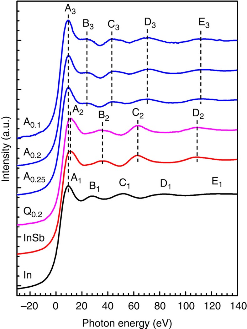
We compare In K-edge X-ray absorption near-edge structure (XANES) experimental spectra of quenched In0.2Co4Sb12 (Q0.2) and annealed InxCo4Sb12 (x=0.1, 0.2 and 0.25) (Ax) with those of InSb and In metal (Fig. 1). The In K-edge XANES spectrum of the In metal has five absorption peaks A1, B1, C1, D1 and E1 centred at about 9, 28, 52, 84 and 128 eV, respectively, whereas that of InSb has four absorption peaks A2, B2, C2 and D2 at about 11, 35, 64 and 107 eV, respectively. The In K-edge XANES spectrum of Q0.2 has four absorption peaks with almost the same positions as those of InSb, indicating the existence of InSb in Q0.2.
Figure 1. The In K-edge XANES experimental spectra.
The quenched In0.2Co4Sb12 is symbolized with ‘Q0.2’. The annealed InxCo4Sb12 (x=0.1, 0.2 and 0.25) is symbolized with ‘Ax’. The In K-edge XANES experimental spectra of InSb and In metals are plotted for comparison. Zero eV corresponds to the threshold of In K-edge (27,940 eV).
All the In K-edge XANES spectra of the Ax samples encompass five absorption peaks A3, B3, C3, D3 and E3 with energy near 9, 23, 42, 70 and 113 eV, respectively. The main peak A3 has the same energy as that of A1 for the In metal, but is 2 eV lower than that of A2 for InSb. For the In K-edge XANES spectra, the main peaks A1, A2 and A3 can be attributed to the 1s→5p transition. The energy discrepancy of A2 and A3 indicates that the chemical states of the In impurity are different between the Ax samples and InSb. It is worth noting that the absorption peaks B3, C3, D3 and E3 of all the Ax samples are distinctly different in energy from B1, C1, D1 and E1 for the In metal, and from B2, C2 and D2 of InSb. Such significant differences undoubtedly show that the In impurities in the Ax samples are neither InSb nor the In metal. Accordingly, it is highly plausible that the In impurities have been incoporated in the lattice of CoSb3 in all annealed samples, well consistent with the X-ray diffraction results (see Supplementary Fig. 1).
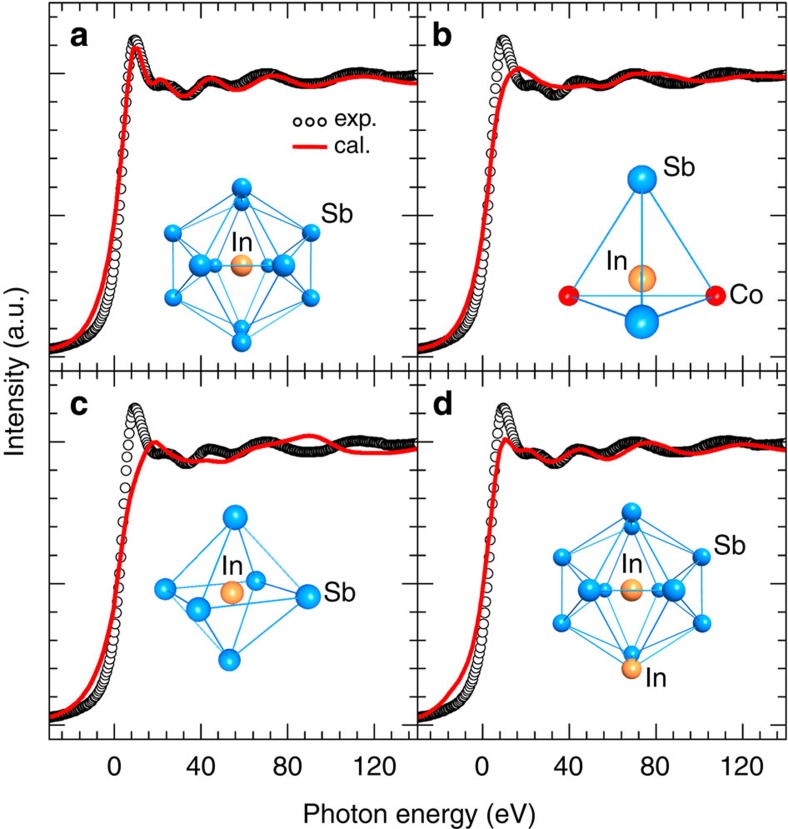
Because of the close electronegativity values among In (1.78), Sb (2.05) and Co (1.88), there exist four possible occupational sites for the In impurities in CoSb3, filling the icosahedron voids at the 2a sites to form In-filled CoSb3, substituting for Sb at the 24g sites in the disordered Sb2Co2 tetrahedron to form In-doped CoSb3−sIns, substituting for Co at the 8c sites in the irregular Sb6 octahedron to form In-doped Co1−rInrSb3 or simultaneously filling the icosahedron voids at the 2a sites and substituting for Sb at the 24g sites to form (InVF)x2/3Co4Sb12−x/3(InSb)x/3 with charge-compensated compound defects33. The In K-edge XANES theoretical spectra of the In impurities at the 2a, 24g, 8c and 2a–24g sites in CoSb3 were calculated to identify which sites the In impurities occupy. The In K-edge XANES theoretical spectra (red solid lines symbolize ‘cal.’) of In-filled CoSb3 for the In impurities (a) filling icosahedron voids at the 2a sites, (b) substituting for Sb at the 24g sites, (c) substituting for Co at 8c sites and (d) simultaneously filling the icosahedron voids at the 2a sites and substituting for Sb at the 24g sites are compared with the experimental spectrum (circle lines symbolize ‘exp.’) of the A0.25 sample (Fig. 2). It is clear that only the In K-edge XANES theoretical spectrum for filling icosahedron voids is in good agreement with the experimental data; the other three cases have large discrepencies between the theoretical spectra and the experimental ones (Fig. 2b–d). Therefore, the In K-edge XANES spectra unequivocally suggest that the In impurities stably fill the Sb12 icosahedron voids in CoSb3.
Figure 2. The In K-edge XANES spectra of In impurity in CoSb3.
(a) Filling Sb12 icosahedron voids at the 2a sites, (b) substituting for Sb at the 24g sites, (c) substituting for Co at the 8c sites and (d) simultaneously filling the icosahedron voids at the 2a sites and substituting for Sb at the 24g sites. The In K-edge XANES experimental spectra of A0.25 are plotted for comparison. The XANES theoretical spectra are shown with red solid lines and symbolized as ‘cal.’. The XANES experimental ones are shown with black circle lines and symbolized as ‘exp.’.
5p-orbital hybridization between In and Sb and its effects
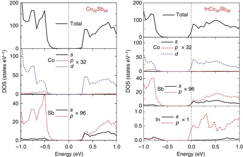
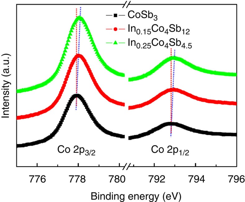
The total DOSs of CoSb3 and In0.125Co4Sb12, and partial DOS for Co, Sb and In atoms indicate that the total DOS of In-filled In0.125Co4Sb12 near valence band maximum (VBM) and conduction band minimum (CBM) mainly stem from Co 3d electrons and Sb 5p electrons (Fig. 3). It can be seen that there is an extra peak of the partial DOS of Co 3d and Sb 5p electrons near 0.31 eV for In0.125Co4Sb12, which exactly corresponds to the highest peak of the partial DOS of In 5p electrons. Particularly, the DOSSb5p/DOSCo3d ratio is decreased near VBM from 2.96 for CoSb3 to 2.08 for In0.125Co4Sb12 and increased near CBM from 0.20 for CoSb3 to 0.22 for In0.125Co4Sb12. This evolution suggests that the energy of Sb 5p electrons and Co 3d electrons becomes closer, and the p–d orbital hybridization between Co and Sb has thus been enhanced in In0.125Co4Sb12. Experimentally, the XPS spectra of Co 2p3/2 and 2p1/2 core levels of In-filled CoSb3 are gradually shifted to higher binding energies (maximum up to 0.20 eV) as the filling fraction of the In filler increased (Fig. 4). The chemical shift is less than the energy resolution of XPS (about 0.47 eV) due to too low filling fraction of the In filler; however, the chemical shift can be repeated (see Supplementary Fig. 2) and thus may provide a plausible evidence of enhanced p–d orbital hybridization between Co and Sb.
Figure 3. Total DOS and partial DOS near VBM and CBM of CoSb3 and In0.125Co4Sb12.
The 2 × 2 × 2 supercells were calculated using projector-augmented wave method implemented in CASTEP package based on the density functional theory.
Figure 4. XPS spectra of Co 2p3/2 and 2p1/2 core levels for CoSb3 and In-filled CoSb3.
Measurements were performed under the CAE mode with pass energy of 25 eV, step size of 0.05 eV and 128 scans with a Thermo VG Multilab 2000 spectrometer.
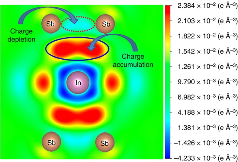
To clarify the origin of enhanced p–d orbital hybridization between Co and Sb in In-filled CoSb3, the partial DOS of In atoms in the range of −12~2 eV have been analysed. We discover that the partial DOS of In 5s electrons are distributed about 1.0 eV below the Fermi level (see Supplementary Fig. 3). Therefore, all In 5s electrons are confined at the deep locations of the valence band and have no contribution to n. Although there are a few In 5p electrons below the Fermi level, the partial DOS of In 5p electrons are mainly distributed above and near the Fermi level, suggesting that the In 5p electrons are almost lost in In-filled CoSb3. The electronic states of the In impurity clearly show that the effective charge of the In filler is smaller than, but very close to, +1. Therefore, the electronic configuration of the In filler is 5s24d105p0, suggesting that the In filler may provide three unoccupied 5p orbitals for a 5p-orbital hybridization between In and Sb. This is corroborated by the differential charge density of In0.125Co4Sb12 projected on the (111) plane (Fig. 5) clearly showing the 5p-orbital hybridization between In and Sb in In-filled CoSb3. Therefore, the enhancement in p–d orbital hybridization between Co and Sb in In-filled CoSb3 must originate from the 5p-orbital hybridization between In and Sb. Note that the charge density decreases between Sb and Sb atoms while it increases between In and Sb atoms for In-filled icosahedron voids, indicating that the partial charges are transferred from Sb to In, which are in good agreement with our previous XPS results27. Namely, the 5p-orbital hybridization between In and Sb in In-filled CoSb3 can still cause a charge transfer from Sb to In and produce two types of atomic-scale electric fields near the In-filled Sb12 icosahedron, which are the atomic-scale electric fields with positive charge at the framework of In-filled Sb12 icosahedron and the atomic-scale electric fields with negative charge in the Sb12 icosahedron. Since the framework of Sb12 icosahedron acts as the passage of majority carriers (electrons) in In-filled CoSb3, the atomic-scale electric fields with positive charge at the framework of In-filled Sb12 icosahedron may accelerate electron movement.
Figure 5. Differential charge density of In0.125Co4Sb12 projected on the (111) plane.
The 2 × 2 × 2 supercells were calculated using the projector-augmented wave method implemented in CASTEP package based on the density functional theory. The differential charge density. delta p=pInCo32Sb96−pCo32Sb96−pIn
In–Sb weak covalent bond and its effects
The extended XAFS (EXAFS) analysis reveals that the In–Sb bond length is about 3.35 Å for the A0.2 sample (see Supplementary Fig. 4) and very close to the value (3.36 Å) reported for In0.2Co4Sb12 (ref. 34), while it is only about 2.81 Å for InSb43. The longer In–Sb bond indicates less orbital overlapping and weakened repulsion interaction between bonding and antibonding states of In–Sb bond in In-filled CoSb3. Therefore, the In–Sb bond between In filler and host framework of Sb12 icosahedron must be a weak covalent bond in In-filled CoSb3, further corroborating the lower energy of the main peak A3 than that of A2 (Fig. 1). Obviously, the In fillers can rattle inside the voids and cause heat-carrying phonon-localized resonant scattering, thereby remarkably reducing κL.
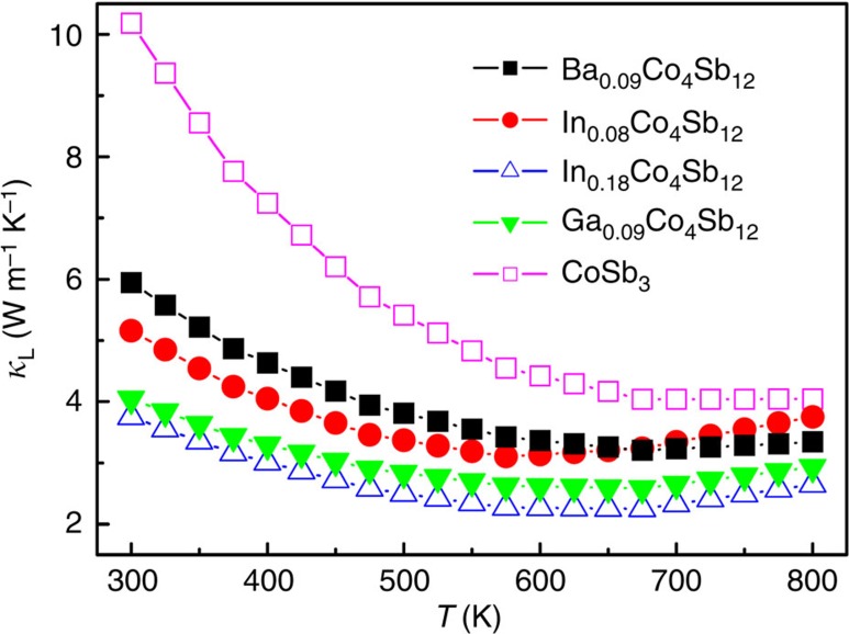
The temperature dependences of κL values for CoSb3 and In-, Ba- and Ga-filled CoSb3 (Fig. 6) show that κL value at 300 K is only about 5.16 W m−1 K−1 for In0.08Co4Sb12 and 3.75 W m−1 K−1 for In0.18Co4Sb12 while more than 10 W m−1 K−1 for CoSb3. The κL values of In0.08Co4Sb12 are smaller than those of Ba0.09Co4Sb12 in the range of 300–650 K, suggesting that the In filler is more effective in reducing κL than Ba at a comparable filling fraction. The κL values of In0.08Co4Sb12, however, are significantly greater than those of Ga0.09Co4Sb12 in the range of 300–800 K, suggesting different doping behaviour in CoSb3 between In and Ga. The lower κL values of Ga0.09Co4Sb12 are due to the additional defect scattering induced by the Sb-substitutional Ga, because Ga impurties in CoSb3 were thought to simultaneously occupy both the icosahedron voids and the Sb sites32.
Figure 6. Temperature dependences of lattice thermal conductivity in the range of 300–800 K.
The data of CoSb3 are plotted for comparison with those of In-, Ba-, and Ga-filled CoSb3.
Discussion
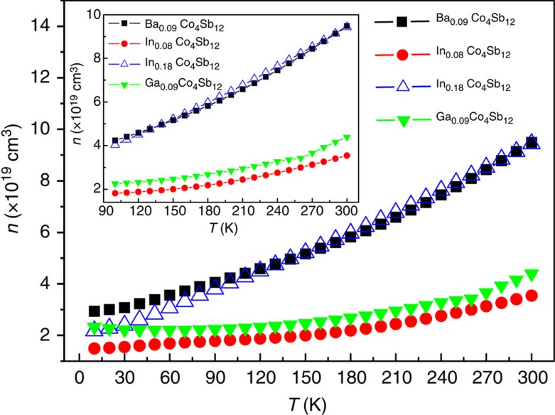
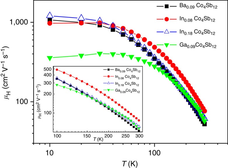
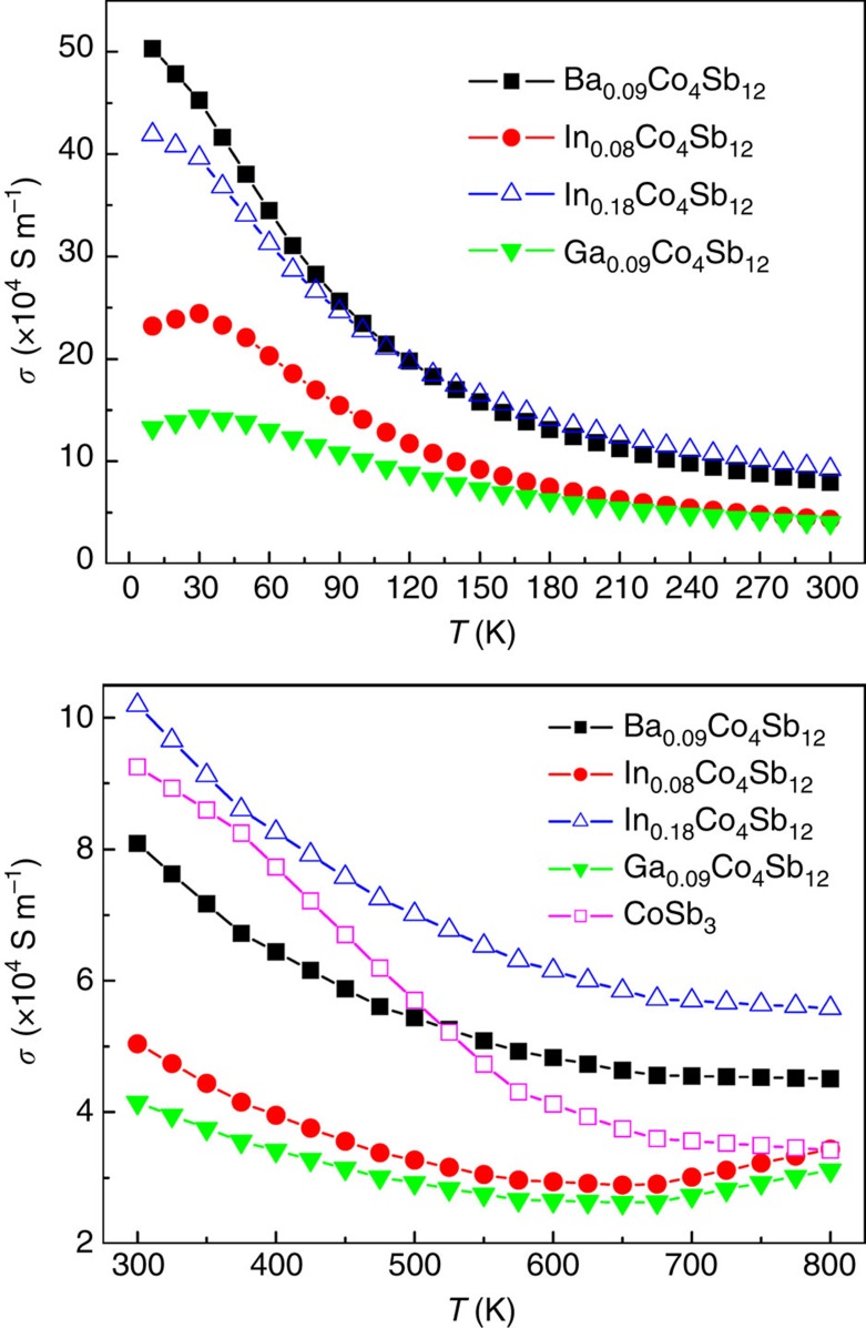
The n values of In0.18Co4Sb12 are almost the same as those of Ba0.09Co4Sb12 in the range of 100–300 K (Fig. 7), clearly indicating that the In filler provides one electron and is univalent (In+) in In-filled CoSb3 because the Ba filler provides two electrons in Ba-filled CoSb3. The electronic structure of the In filler described above not only is the physical mechanism of low n for In-filled CoSb3, but also may reasonably explain why the n values of In0.18Co4Sb12 and Ba0.09Co4Sb12 are very close in the range of 100–300 K. At the same time, the charge transfer from Sb to In in In-filled CoSb3 must produce the same amount of atomic-scale electric fields with positive charge at the framework of In-filled Sb12 icosahedron; therefore, the major carriers (electrons) nearby the In-filled Sb12 icosahedron are not only partially annihilated but also accelerated because of the attraction by the atomic-scale electric fields with positive charge. These multi-functional local transport effects may explain that the In-filled CoSb3 has higher μH than those of Ba-filled and Ga-filled CoSb3 in the range of 100–300 K under comparable n values (Fig. 8). As a result, the In-filled CoSb3 have higher σ than Ba- and Ga-filled CoSb3 in the range of 150–800 K, although their n values are very close (Fig. 9), which can be attributed to an increase in μH induced by accelerated electron movement nearby the In-filled Sb12 icosahedron. Compared with Ba- and In-filled CoSb3, the lower μH of Ga-filled CoSb3 in the range of 10–100 K may be reasonably explained by the dual-site occupancy of Ga impurity in CoSb3 (ref. 32). In addition, the μH values of Ba- and In-filled CoSb3 share similar temperature dependence in the range of 10–300 K (Fig. 8), implying that the electron scattering mechanisms are the same for both cases and there is thus no case of In occupying at the Sb sites. This is well consistent with the XANES results as shown in Fig. 2.
Figure 7. Temperature dependences of carrier concentration in the range of 10–300 K.
The inset shows the temperature dependences of carrier concentration of In-, Ba-, and Ga-filled CoSb3 in the range of 100–300K.
Figure 8. Temperature dependences of Hall mobility in the range of 10–300 K.
The inset shows the temperature dependences of Hall mobility of In-, Ba-, and Ga-filled CoSb3 in the range of 100–300K.
Figure 9. Temperature dependences of electrical conductivity in the range of 10–800 K.
The data of CoSb3 in the range of 300–800K are plotted for comparison with those of In-, Ba-, and Ga-filled CoSb3.
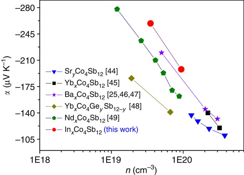
The enhancement of the p–d orbital hybridization between Co and Sb induced by the In filler still provides a more reasonable explanation for the band structure of In0.125Co4Sb12. Compared with CoSb3 (see Supplementary Fig. 5), the Fermi level of In0.125Co4Sb12 is migrated into conduction bands and the energy gap between the Fermi level and CBM at H, N and P points with high symmetry is significantly decreased from 0.45~0.35 eV for CoSb3 to 0.12~0.03 eV for In0.125Co4Sb12. As a result, the DOS of VBM is significantly decreased while the DOS of CBM is remarkably increased. Namely, there is an asymmetric distribution of DOS near the Fermi level of In-filled CoSb3 beneficial to obtaining a large α. Such a DOS asymmetric distribution may very well explain why the absolute α values of In-filled CoSb3 are higher than those of n-type Ba-, Sr-, Yb- and Nd-filled CoSb3, with similar n on the order of 1019 cm−3 at room temperature25,44,45,46,48,49, as shown in Fig. 10. The α values at 300 K reached 259 μV K−1 for In0.08Co4Sb12 with 3.5 × 1019 cm−3 and 198 μV K−1 for In0.18Co4Sb12 with 9.4 × 1019 cm−3. Obviously, the large α values of In-filled CoSb3 originate from the increase in DOS of CBM near the Fermi level due to enhanced p–d orbital hybridization between Co and Sb induced by the In filler.
Figure 10. Carrier concentration dependences of the Seebeck coefficient of n-type filled CoSb3 at room temperature.
Here, compare the data of Sr-, Yb-, Ba-, Nd-, and In-filled CoSb3 with n on the order of 1019~1020 cm−3.
Therefore, the perfect combination of low κL, high σ and large α for In-filled CoSb3 originates from the following physical and chemical mechanisms. First, the low κL is due to the heat-carrying phonon-localized resonant scattering induced by In-filler rattling. Second, the high σ is attributed to the accelerated electron movement induced by the charge transfer from Sb to In. Third, the large α benefits from the increase in DOS of CBM near the Fermi level induced by the enhanced p–d orbital hybridization between Co and Sb. The 5p-orbital hybridization between In and Sb in In-filled CoSb3 can cause a charge transfer from Sb to In and the enhancement of p–d orbital hybridization between Co and Sb. The fundamental origin of low n of In-filled CoSb3 is that all 5s electrons of the In filler are confined at the deep locations of the valence band. The low n and asymmetric distribution of DOS near the Fermi level provide a favourable condition for adjusting σ and α of In-filled CoSb3 in an independent way.
Methods
Synthesis and characterization
In-filled InxCo4Sb12 (x=0.1, 0.2 and 0.25) bulk materials were prepared by a combination of melting, annealing and spark plasma sintering reported elsewhere25. Another three bulk materials (CoSb3, Ba0.1Co4Sb12 and Ga0.1Co4Sb12) were prepared with the same method for comparsion. X-ray diffraction (PANalytical X’ Pert PRO) and scanning electron microscope analysis confirmed that all the annealed samples InxCo4Sb12 (x=0.1, 0.2 and 0.25) were composed of single-phase skutterudite, while all the quenched samples consisted of Sb, CoSb, CoSb2 and InSb. Chemical compositions of all the bulk materials were determined by electron probe microanalysis (EPMA, JXA-8230). XANES and EXAFS of quenched In0.2Co4Sb12 and annealed InxCo4Sb12 samples were measured under a working voltage of 3.5 GeV and a working current of 300 mA at BL14W1 beamline in the Shanghai Synchrotron Radiation Facility (SSRF). A Si (311) double-crystal monochromater with energy resolution of 0.5 × 10⁻⁴ eV@10 keV was employed to measure In K-edge spectra. All XANES and EXAFS spectra were measured three times to ensure reproducibility. The In K-edge XANES spectra of InSb and the In metal were also recorded for comparison. XPS of Co 2p3/2 and 2p1/2 core levels were recorded at pass energy of of 25 eV, step size of 0.05 eV and 128 scans with Thermo VG Multilab 2000 spectrometer.
Transport measurement
The σ and α values were measured with the standard four-probe method (UlvacRiko: ZEM-3) in Ar atmosphere. The κ was calculated using the equation κ=DρCp, where Cp is the specific heat capacity, ρ the bulk density and D the thermal diffusion coefficient. D was measured by a laser flash technique (Netzsch LFA 427) in a flowing Ar atmosphere, Cp with a TA Q20 differential scanning calorimeter and ρ by Archimedes method. κL was obtained by subtracting the electrical contribution from κ using the equation κL=κ−κE. κE is expressed by the Wiedemann–Franz κE=σLT, where L is the Lorenz number. Uncertainties are ±5–7% for σ and κL, and ±5% for α. The n and μH were measured under 10–300 K with Quantum Design PPMS.
Theoretical calculation
The K-edge XANES theoretical spectra of In impurity at four kinds of crystallographic sites (2a, 24g, 8c and 2a–24g) in CoSb3 were calculated with the self-consistent multiple-scattering theory based on real-space clusters implemented in FEFF9 package50. The In K-edge EXAFS experimental spectra were first normalized and background subtracted to obtain the k-weighted spectra, and then Fourier transformed to obtain the length of the In–Sb bond. The DOSs, band structure and differential charge densities projected on the (111) plane of CoSb3 and In0.125Co4Sb12 using a 2 × 2 × 2 supercell were calculated using a projector-augmented wave method implemented in CASTEP package based on the density functional theory51. Lattice relaxation and structural optimization were carried out through total energy calculations.
Author contributions
W.Z., P.W. and Q.Z. designed and carried out XANES and EXAFS experiments. P.W., W.Z., D.T., J.Y., H.Z. and Z.L. synthesized the samples and carried out the thermoelectric properties measurements. H.P., J.L. and C.W. performed the electron structure calculations. W.Z., P.W., W.Z., X.T. and J.Y. performed the Hall measurements. W.Z. and D.T. performed the XPS measurements. W.Z., P.W., Q.Z and J.Y. conceived the experiments, analysed the results and wrote and edited the manuscript. All authors read the paper and commented on the text.
Additional information
How to cite this article: Zhao, W. et al. Multi-localization transport behaviour in bulk thermoelectric materials. Nat. Commun. 6:6197 doi: 10.1038/ncomms7197 (2015).
Supplementary Material
Supplementary Figures 1-5
Acknowledgments
This work was supported by the National Basic Research Program of China (973 program) under Project No. 2013CB632505, and National Natural Science Foundation of China (Nos 50930004, 50972114 and 11274248). XANES and EXAFS measurements were performed at BL14W1 beamline in Shanghai Synchrotron Radiation Facility. XRD, SEM and EPMA experiments were performed at the Center for Materials Research and Testing of Wuhan University of Technology. Hall measurements were performed at US General Motors Corp. and State Key Lab of Advanced Technology for Materials Synthesis and Processing of Wuhan University of Technology. X-ray photoemission spectra were recorded at Key Laboratory of Catalysis and Materials Science of the State Ethnic Affair Commission & Ministry of Education of South-Central University for Nationalities and School of Physics and Technology of Wuhan University. We thank Dr Zhang and Professor Jiang for their help in XANES and EXAFS measurements. We also thank Professor G.S. Shao from the University of Bolton for the valuable discussions on XANES and EXAFS analysis; thanks to Professor L.M. Mei from Shandong University, Professor J. Shi and Professor H.J. Liu from Wuhan University and Professor X.M. Min from Wuhan University of Technology for their valuable discussions on the electronic structure of In-filled CoSb3.
References
- Bell L. E. Cooling, heating, generating power, and recovering waste heat with thermoelectric systems. Science 321, 1457–1461 (2008). [DOI] [PubMed] [Google Scholar]
- Snyder G. J. & Toberer E. S. Complex thermoelectric materials. Nat. Mater. 7, 105–114 (2008). [DOI] [PubMed] [Google Scholar]
- Biswas K. et al. High-performance bulk thermoelectrics with all-scale hierarchical architectures. Nature 489, 414–418 (2012). [DOI] [PubMed] [Google Scholar]
- Hsu K. F. et al. Cubic AgPbmSbTe2+m: Bulk thermoelectric materials with high figure of merit. Science 303, 818–821 (2004). [DOI] [PubMed] [Google Scholar]
- Dresselhaus M. S. et al. New directions for low-dimensional thermoelectric materials. Adv. Mater. 19, 1043–1053 (2007). [Google Scholar]
- Poudel B. et al. High-thermoelectric performance of nanostructured bismuth antimony telluride bulk alloys. Science 320, 634–638 (2008). [DOI] [PubMed] [Google Scholar]
- Morelli D. T., Jovovic V. & Heremans J. P. Intrinsically minimal thermal conductivity in cubic I-V-VI2 semiconductors AgSbTe2 and AgBiSe2. Phys. Rev. Lett. 101, 035901-1–035901-4 (2008). [DOI] [PubMed] [Google Scholar]
- Sales B. C., Mandrus D. & Williams R. K. Filled skutteruditeantimonides: a new class of thermoelectric materials. Science 272, 1325–1328 (1996). [DOI] [PubMed] [Google Scholar]
- Siemens M. E. et al. Quasi-ballistic thermal transport from nanoscale interfaces observed using ultrafast coherent soft X-ray beams. Nat. Mater. 9, 26–30 (2010). [DOI] [PubMed] [Google Scholar]
- Zhao W. Y. et al. Enhanced thermoelectric performance via randomly arranged nanopores: excellent transport properties of YbZn2Sb2 nanoporous materials. Acta Mater. 60, 1741–1746 (2012). [Google Scholar]
- Liu H. L. et al. Copper ion liquid-like thermoelectric. Nat. Mater. 11, 422–425 (2012). [DOI] [PubMed] [Google Scholar]
- Delaire O. et al. Giant anharmonic phonon scattering in PbTe. Nat. Mater. 10, 614–619 (2011). [DOI] [PubMed] [Google Scholar]
- Pei Y. Z. et al. Convergence of electronic bands for high performance bulk thermoelectric. Nature 473, 66–69 (2011). [DOI] [PubMed] [Google Scholar]
- Liu W. et al. Convergence of conduction bands as a means of enhancing thermoelectric performance of n-type Mg2Si1−xSnx solid solutions. Phys. Rev. Lett. 108, 166601–166605 (2012). [DOI] [PubMed] [Google Scholar]
- Rhyee J. S. et al. Peierls distortion as a route to high thermoelectric performance in In4Se3-delta crystals. Nature 459, 965–968 (2009). [DOI] [PubMed] [Google Scholar]
- Heremans J. P. et al. Enhancement of thermoelectric efficiency in PbTe by distortion of the electronic density of states. Science 321, 554–557 (2008). [DOI] [PubMed] [Google Scholar]
- Ahmad S., Hoang K. & Mahanti S. D. Ab Initio study of deep defect states in narrow band-gap semiconductors: Group III impurities in PbTe. Phys. Rev. Lett. 96, 056403-1–056403-4 (2006). [DOI] [PubMed] [Google Scholar]
- Lee J.-H., Wu J. & Grossman J. C. Enhancing the thermoelectric power factor with highly mismatched isoelectronic doping. Phys. Rev. Lett. 104, 016602-1–066602-4 (2010). [DOI] [PubMed] [Google Scholar]
- Zhou J., Yang R. G., Chen G. & Dresselhaus M. S. Optimal bandwidth for high efficiency thermoelectric. Phys. Rev. Lett. 107, 226601-1–226601-5 (2011). [DOI] [PubMed] [Google Scholar]
- Nolas G. S., Cohn J. L. & Slack G. A. Effect of partial void filling on the lattice thermal conductivity of skutterudites. Phys. Rev. B 58, 164–170 (1998). [Google Scholar]
- Uher C. inRecent Trends in Thermoelectric Materials Research I, Semiconductors and Semimetals ed. Tritt T. M. Vol. 69139–253Academic Press (2001). [Google Scholar]
- Nolas G. S., Kaeser M., Littleton R. T. & Tritt T. M. High figure of merit in partially filled ytterbium skutterudite materials. Appl. Phys. Lett. 77, 1855–1857 (2000). [Google Scholar]
- Morelli D. T., Meisner G. P., Chen B. X., Hu S. Q. & Uher C. Cerium filling and doping of cobalt triantimonide. Phys. Rev. B 56, 7376–7383 (1997). [Google Scholar]
- Chen L. D. et al. Anomalous barium filling fraction and n-type thermoelectric performance of BayCo4Sb12. J. Appl. Phys. 90, 1864–1868 (2001). [Google Scholar]
- Zhao W. Y. et al. Synthesis and high temperature transport properties of barium and indium double-filled skutterudites BaxInyCo4Sb12−z. J. Appl. Phys. 102, 113708-1–113708-6 (2007). [Google Scholar]
- Pei Y. Z. et al. Improving thermoelectric performance of caged compounds through light-element filling. Appl. Phys. Lett. 95, 042101-1–042101-3 (2009). [Google Scholar]
- Zhao W. Y. et al. Enhanced thermoelectric performance in barium and indium double-filled skutterudite bulk materials via orbital hybridization induced by indium filler. J. Am. Chem. Soc. 131, 3713–3720 (2009). [DOI] [PubMed] [Google Scholar]
- Shi X. et al. Multiple-filled skutterudites: high thermoelectric figure of merit through separately optimizing electrical and thermal transports. J. Am. Chem. Soc. 133, 7837–7846 (2011). [DOI] [PubMed] [Google Scholar]
- Mei Z. G., Yang J., Pei Y. Z., Zhang W. & Chen L. D. Alkali-metal-filled CoSb3 skutterudites as thermoelectric materials: theoretical study. Phys. Rev. B 77, 045202-1–045202-8 (2008). [Google Scholar]
- Sales B. C., Chakoumakos B. C. & Mandrus D. Thermoelectric properties of thallium-filled skutterudites. Phys. Rev. B 61, 2475–2481 (2000). [Google Scholar]
- Hermann R. P. et al. Einstein oscillators in thallium filled antimony skutterudites. Phys. Rev. Lett. 90, 135505-1–135505-4 (2003). [DOI] [PubMed] [Google Scholar]
- Qiu Y. T. et al. Charge-compensated compound defects in Ga-containing thermoelectric skutterudites. Adv. Funct. Mater. 23, 3194–3203 (2013). [Google Scholar]
- Tang Y. L. et al. Phase diagram of In–Co–Sb system and thermoelectric properties of In-containing skutterudites. Energy Environ. Sci. 7, 812–819 (2014). [Google Scholar]
- He T., Chen J. Z., Rosenfeld H. D. & Subramanian M. A. Thermoelectric properties of indium-filled skutterudites. Chem. Mater. 18, 759–762 (2006). [Google Scholar]
- Harnwunggmoung A. et al. Enhancement of thermoelectric properties of CoSb3-based skutterudites by double filling of Tl and In. J. Appl. Phys. 112, 043509-1–043509-6 (2012). [Google Scholar]
- Wang L., Cai K. F., Wang Y. Y., Li H. & Wang H. F. Thermoelectric properties of indium-filled skutterudites prepared by combining solvothermal synthesis and melting. Appl. Phys. A 97, 841–845 (2009). [Google Scholar]
- Wei P. et al. Excellent performance stability of Ba and In double-filled skutterudite thermoelectric materials. Acta Mater. 59, 3244–3254 (2011). [Google Scholar]
- Yu J. et al. Effect of In impurity on thermoelectric properties of Ba and In double-filled n-type skutterudite materials. J. Electron. Mater. 41, 1395–1400 (2012). [Google Scholar]
- Peng J. Y. et al. High temperature thermoelectric properties of double-filled InxYbyCo4Sb12 skutterudites. J. Appl. Phys. 105, 084907-1–084907-5 (2009). [Google Scholar]
- Grytsiv A., Rogl P., Michor H., Bauer E. & Giester G. InyCo4Sb12 skutterudite: Phase equilibria and crystal structure. J. Electron. Mater. 42, 2940–2952 (2013). [Google Scholar]
- Eilertsen J., Rouvimov S. & Subramanian M. A. Rattler-seeded InSb nanoinclusions from metastable indium-filled In0.1Co4Sb12 skutterudites for high-performance thermoelectric. Acta Mater. 60, 2178–2785 (2012). [Google Scholar]
- Li H., Tang X. F., Zhang Q. J. & Uher C. High performance InxCeyCo4Sb12 thermoelectric materials with in situ forming nanostructured InSb phase. Appl. Phys. Lett. 94, 102114-1–102114-3 (2009). [Google Scholar]
- Chen D. L., Li C. S., Zhu Z. G., Fan J. W. & Wei S. Q. Interface effect of InSb quantum dots embedded in SiO2 matrix. Phys. Rev. B 72, 075341-1–075341-7 (2005). [Google Scholar]
- Zhao X. Y. et al. Synthesis and thermoelectric properties of Sr-filled skutterudite SryCo4Sb12. J. Appl. Phys. 99, 053711-1–053711-4 (2006). [Google Scholar]
- Li H., Tang X. F., Su X. L., Zhang Q. J. & Uher C. Nanostructured bulk YbxCo4Sb12 with high thermoelectric performance prepared by the rapid solidification method. J. Phys. D Appl. Phys. 42, 145409-1–145409-9 (2009). [Google Scholar]
- Bai S. Q. et al. Enhanced thermoelectric performance of dual-element-filled skutterudites BaxCeyCo4Sb12. Acta Mater. 57, 3135–3139 (2009). [Google Scholar]
- Shi X. et al. Low thermal conductivity and high thermoelectric figure of merit in n-type BaxYbyCo4Sb12 double-filled skutterudites. Appl. Phys. Lett. 92, 182101-1–182101-3 (2008). [Google Scholar]
- Lamberton G. A. Jr., Tedstrom R. H., Tritt T. M. & Nolas G. S. Thermoelectric properties of Yb-filled Ge-compensated CoSb3 skutterudite materials. J. Appl. Phys. 97, 113715-1–113715-5 (2005). [Google Scholar]
- Kuznetsov V. L., Kuznetsova L. A. & Rowe D. M. Effect of partial void filling on the transport properties of NdxCo4Sb12 skutterudites. J. Phys Condens. Matter. 15, 5035–5048 (2003). [Google Scholar]
- Rehr J. J. & Albers R. C. Theoretical approaches to X-ray absorption fine structure. Rev. Mod. Phys. 72, 621–654 (2000). [Google Scholar]
- Payne M. C., Teter M. P., Allan D. C., Arias T. A. & Joannopoulos J. D. Iterative minimization techniques for ab initio total-energy calculations: molecular dynamics and conjugate gradients. Rev. Mod. Phys. 64, 1045–1097 (1992). [Google Scholar]
Associated Data
This section collects any data citations, data availability statements, or supplementary materials included in this article.
Supplementary Materials
Supplementary Figures 1-5


