Abstract
For the application of colloidal semiconductor quantum dots in optoelectronic devices, for example, solar cells and light-emitting diodes, it is crucial to understand and control their charge transport and recombination dynamics at high carrier densities. Both can be studied in ambipolar, light-emitting field-effect transistors (LEFETs). Here, we report the first quantum dot light-emitting transistor. Electrolyte-gated PbS quantum dot LEFETs exhibit near-infrared electroluminescence from a confined region within the channel, which proves true ambipolar transport in ligand-exchanged quantum dot solids. Unexpectedly, the external quantum efficiencies improve significantly with current density. This effect correlates with the unusual increase of photoluminescence quantum yield and longer average lifetimes at higher electron and hole concentrations in PbS quantum dot thin films. We attribute the initially low emission efficiencies to nonradiative losses through trap states. At higher carrier densities, these trap states are deactivated and emission is dominated by trions.
Keywords: PbS, quantum dot, ambipolar, light-emitting transistor, electroluminescence, trion
Semiconducting colloidal quantum dots (QDs) are attractive materials for solution-processed optoelectronic devices including solar cells,1−3 photodetectors,4−6 field-effect transistors (FETs),7−11 and light-emitting diodes (LEDs).12−15 For these QD-based devices, where charge carrier densities can be high and influence the optoelectronic properties, a fundamental understanding of charge transport and recombination dynamics is necessary. An excellent system to investigate these effects is an ambipolar light-emitting field-effect transistor (LEFET). In an ambipolar FET, holes and electrons are injected into the channel from the source and drain electrodes, respectively, depending on the biasing conditions.16 The formed accumulation layers meet within the channel resulting in electron–hole recombination and thus light emission from a narrow line, the recombination zone. The position of the recombination zone depends on the applied gate and source-drain voltage and can be moved arbitrarily through the entire channel. When the emission zone is located away from the electrodes all injected holes and electrons must recombine. Thus, hole and electron currents are always perfectly balanced without the need for hole or electron blocking layers. One of the most important features of LEFETs is the charge carrier density, which can be orders of magnitude higher than in diodes and thus allows for the investigation of recombination and emission dynamics large carrier concentrations. Ambipolar LEFETs have so far been demonstrated for bulk organic semiconductors (conjugated polymers17 and single crystals18), two-dimensional semiconductors (e.g., transition metal dichalcogenides like WS219 or MoS220), and one-dimensional semiconductors (individual single-walled carbon nanotubes21 and networks22). However, LEFETs based on zero-dimensional semiconductors have so far remained elusive, either due to insufficient ambipolar charge transport or severe Auger quenching of emission in thin films. They are the last missing example to demonstrate the universality of ambipolar transport and light-emission in field-effect transistors. PbS QDs are ideal candidates for the realization of quantum dot light-emitting FETs. They exhibit good photoluminescence yields and size-tunable emission wavelengths in the near-infrared (800–1800 nm)23 and have been applied in LEDs as alternatives to traditional InGaAsP light-emitting diodes.15,24 They have a small bandgap and a large Bohr radius (∼18 nm),25 which facilitates ambipolar charge transport.
Electrolyte-gating is a powerful method to reach high carrier densities for both holes and electrons.26 It enables access to the intrinsic properties of semiconducting QDs by efficient compensation of trap states and dopants.9,11 The dielectric of a conventional top-gated or back-gated transistor is replaced with an electrolyte, which in our case is an iongel based on an ionic liquid. By applying a gate voltage (VG) the anions and cations of the electrolyte move toward the gate electrode and the semiconductor surface, respectively, and form nanometer-thin electric-double layers (EDLs). The applied gate voltage drops over these EDLs, which results in huge effective capacitances (few μF·cm–2), enabling the injection and accumulation of large charge carrier densities (∼1013 cm–2) at very low voltages (<3 V). Electrolyte-gating is especially useful for nanoparticle films because the electrolyte can penetrate the porous particle layers and form EDLs on the surface of each nanoparticle. This hugely enhances the gating effect compared to conventional top- or back-gated geometries.27 Not only the first layer but almost the entire film is charged and thus contributes to the charge transport. Electrolyte-gating can be viewed as an electrochemical doping process where the gate electrode is a polarizable counter electrode, the source/drain electrodes are the working electrode, and the QD film is the electroactive species. Usually, no additional reference electrode is used in electrolyte-gated transistors.
Here, we demonstrate the first quantum dot light-emitting field-effect transistor. We were able to obtain both good ambipolar charge transport and near-infrared light emission using electrolyte-gated PbS QD thin films. Because LEFETs operate at very high carrier densities we also studied the influence of hole and electron accumulation on the recombination dynamics of the PbS QD films by gate voltage-dependent, time-resolved photoluminescence measurements. We propose a model that can explain the significant impact of accumulated charges on the emission efficiencies via deactivation of the nonradiative decay channels and creation of trions as radiative decay channels in ligand-exchanged QD films.
We used different sizes of PbS QDs to create LEFETs including quantum dots with diameters of 4.3 nm (absorption maximum λAbs = 1230 nm; PbS 1), 4.6 nm (λAbs = 1303 nm; PbS 2), and 5.1 nm (λAbs = 1407 nm; PbS 3) as shown in the transmission electron microscopy (TEM) images in Figure 1a and corresponding absorption spectra (Figure 1b). Thin films of these PbS QDs were fabricated via spin-coating in a layer-by-layer (LBL) approach including a ligand exchange of the long capping ligand oleic acid with the short 3-mercaptopropionic acid (MPA). The ligand exchange causes a redshift of the photoluminescence (PL) (see Supporting Information Figure S1) and a substantial decrease in quantum yield (QY). The PL QY drops from relatively high values of around 12% in solution to 1.5–7% for single layer films (with oleic acid) and 0.05–0.07% for ligand-exchanged LBL films. The obtained small interdot spacing promotes efficient charge transport but also leads to reduced QY.15,28
Figure 1.
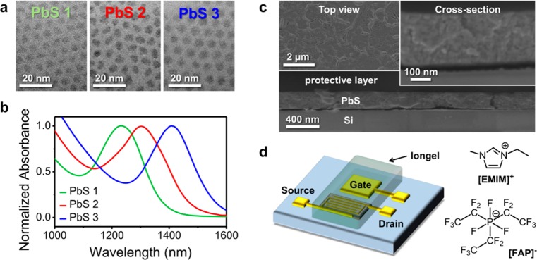
(a) Transmission electron microscopy images of PbS 1 QDs (d ∼ 4.3 nm), PbS 2 QDs (d ∼ 4.6 nm), and PbS 3 QDs (d ∼ 5.1 nm) and (b) corresponding absorption spectra with λPbS1 = 1230 nm (green), λPbS2 = 1303 nm (red), and λPbS3 = 1407 nm (blue). (c) Scanning electron microscopy images of a five layer-by-layer PbS QD film. The top view image shows some surface cracks, the cross-section images reveal a homogeneous layer with a thickness of about ∼230 nm. (d) Schematic illustration of a PbS QD light-emitting field-effect transistor with a side-gate and an iongel electrolyte containing the ionic liquid [EMIM][FAP].
Cross-sectional scanning electron microscopy (SEM) images (Figure 1c) show that the 5 LBL PbS QD films are very homogeneous with a thickness of 220–240 nm. All films show a large number of cracks arising from the volume loss caused by the ligand exchange.29 However, due to crack filling after several LBL steps none of these cracks runs through the entire thickness of the film and continuous charge transport is guaranteed. By annealing the PbS QD films for 30 min at 120 °C these cracks could be removed and carrier mobilities increased but such heat treatment also caused significant broadening and redshift of the emission (see Supporting Information Figure S2) probably due to ligand loss and sintering of the PbS QDs. Hence, all of the following measurements were obtained from nonannealed films.
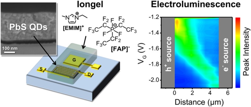
We used electrolyte-gating with an iongel based on the ionic liquid 1-ethyl-3-methyl-imidazolium-tris(pentafluoroethyl)-trifluorophosphate ([EMIM][FAP]) to achieve high charge carrier densities. For simplicity, we employed a side-gate geometry as shown in Figure 1d. Transistors were measured in a nitrogen-filled glovebox and showed clear ambipolar transfer characteristics although with relatively large hysteresis. This hysteresis is typical for PbS and PbSe QD FETs and probably originates from a large number of shallow trap sites.9,10 Figure 2a shows current–voltage characteristics of an LEFET fabricated with PbS 2 QDs (d = 4.6 nm). Field-effect mobilities were estimated from the transconductance at low source-drain voltages (VSD) and ranged from 0.04 to 0.06 cm2 V–1 s–1 for electrons (μe) and 0.003 to 0.009 cm2 V–1 s–1 for holes (μh), assuming a constant capacitance of Ci = 3.4 μF·cm–2 for the iongel. This capacitance value was obtained from measurements of the pure ionic liquid [EMIM][FAP] in a plate–plate geometry with platinum electrodes30 and may differ somewhat from the effective (gate voltage dependent) capacitance of the iongel.
Figure 2.
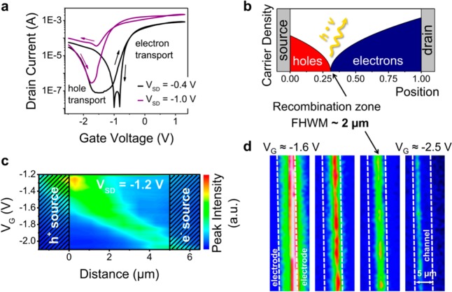
(a) Typical transfer characteristics of an electrolyte-gated FET with spin-coated and ligand-exchanged PbS QDs indicating ambipolar transport. (b) Schematic illustration of hole and electron accumulation and recombination zone for a transistor in the ambipolar regime. (c) Position (distance from hole injecting electrode) and intensity of emission from a PbS QD FET (PbS 2 QDs, channel length L = 5 μm; integration time 10 s) depending on gate voltage for constant source-drain voltage (VSD = −1.2 V) and (d) false-color near-infrared images (wavelengths 800–1600 nm; integration time 5 s) of the recombination and emission zone from the same device at different gate voltages (VSD = −1 V); see also movie in Supporting Information D.
The observed V-shaped transfer curves of PbS QD LEFETs are characteristic for ambipolar transistors. For higher source-drain voltages (VSD) the transfer curves shift due to the altered potential difference between the drain and gate electrode (Figure 2a), which is a typical behavior for ambipolar FETs.16 The output and transfer characteristics of LEFETs fabricated with the three different PbS QDs (see Supporting Information Figure S3) all show the same trend; while sweeping the gate voltage for a constant source-drain bias we observe a transition from unipolar electron accumulation (low positive VG) via the ambipolar regime (low negative VG) to the unipolar hole accumulation regime (high negative VG). The valley of the transfer curve corresponds to the ambipolar regime where both electrons and holes are present in the channel. In this regime, recombination takes place leading to exciton formation and light emission from a confined region in the channel (see scheme in Figure 2b). The position of the resulting emission zone is directly controlled by the applied voltages (Figure 2c,d) and can be moved from the source electrode through the channel to the drain electrode and vice versa (Figure 2c,d, and movie in Supporting Information D). This observation is unambiguous proof for truly ambipolar charge transport and exciton formation by electron–hole recombination in PbS quantum dot films. These PbS QD FETs are thus the first ambipolar, light-emitting FETs based on a zero-dimensional semiconductor.
The emission zone is very uniform and moves through the channel in a straight line, which indicates a homogeneous PbS QD layer and uniform charge injection and transport. The apparent width of the emission zone of about 2 μm (see Supporting Information Figure S4) is partially caused by the limited resolution of the optical setup in the near-infrared. The intensity of emission decreases toward the electron source (see Figure 2c) because of the lower hole mobility in the PbS QD film. This leads to lower currents (as seen in Figure 2a) and thus fewer recombination events when the larger part of the channel is filled with holes. In contrast to electrolyte-gated LEFETs, PbS QD transistors in a top-gate configuration with a thin hafnia dielectric show almost no hole transport. Although electroluminescence can be observed for these devices as well, it is weak and exclusively located at the hole injecting electrode (see Supporting Information Figure S5), which is typical for unipolar LEFETs.
Electroluminescence (EL) and PL spectra from the channel region of the electrolyte-gated FETs are almost indistinguishable (Figure 3a) for all particle sizes. The peak width for all QDs is about 200 nm. We observe a minor redshift of EL versus PL of about 10 nm but no indication of predominant emission from defect states or nanoparticles with larger than average diameters and thus lower energy levels. This further indicates that transport of holes and electrons indeed takes place through the 1Sh and 1Se states of the QDs, respectively. The large gating effect and thus high charge carrier densities enabled by electrolyte-gating facilitate transport through all QDs of the film despite the relatively broad size distribution. The EL spectra did not change at higher current densities.
Figure 3.
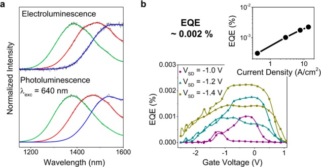
(a) Photoluminescence spectra (excited at 640 nm; ∼10 mW/μm2; integration time 20 s) of PbS QDs (green, PbS 1; red, PbS 2; blue, PbS 3) within the channel region and electroluminescence spectra from the same spot (VG = 0.1 V; VSD = −1.2 V; integration time, 60 s). (b) External quantum efficiency (EQE) of a PbS light-emitting FET (PbS 2) at different source-drain voltages and thus current densities. Inset: maximum EQE versus corresponding current density.
For comparison, PbS QDs with very high PL QYs in solution and more narrow size distributions can be obtained by another synthesis route using PbCl2 and sulfur. Trap sites are passivated by the chlorine anions and a large excess of Pb during particle growth.2,31 However, transistors based on these particles showed very strong electron-doping. Ambipolar currents and thus light emission remained low although measurable with narrow EL and PL peaks (see Supporting Information Figure S6). The emission was largely confined to the hole injecting electrode. Other schemes to increase carrier transport while maintaining high photoluminescence yield, for example, capping PbS nanoparticles with molecular metal chalcogenide complexes32 could potentially increase emission in quantum dot LEFETs but were not investigated in this study.
The external quantum efficiencies (EQE) of LEFETs give further insights into transport and emission properties of PbS QD films at high carrier densities. Our devices exhibit EQEs of about 0.002% (see Figure 3b) for forward emission. These EQE values are comparable with those of PbS QD LEDs fabricated with the same short MPA ligand.15 However, while the EQE of PbS QD LEDs drops at high current densities PbS QD LEFETs exhibit a steady increase in efficiency even beyond current densities of 10 A·cm–2 (taking into account the source-drain current, the total channel width of 20 mm and the full height of the film, i.e., 220 nm). Apparently, additional charges do not lower but improve the quantum yield. This behavior is unexpected because doping is usually associated with quenching of excitons.33−35 Further, photoluminescence measurements of the channel region under constant laser excitation (λexc = 640 nm) at various positive and negative gate voltages and thus electron and hole accumulation, respectively, show a sharp increase in intensity at the threshold voltage for electron and hole transport without any spectral changes (see Figure 4a and Supporting Information Figure S7).
Figure 4.
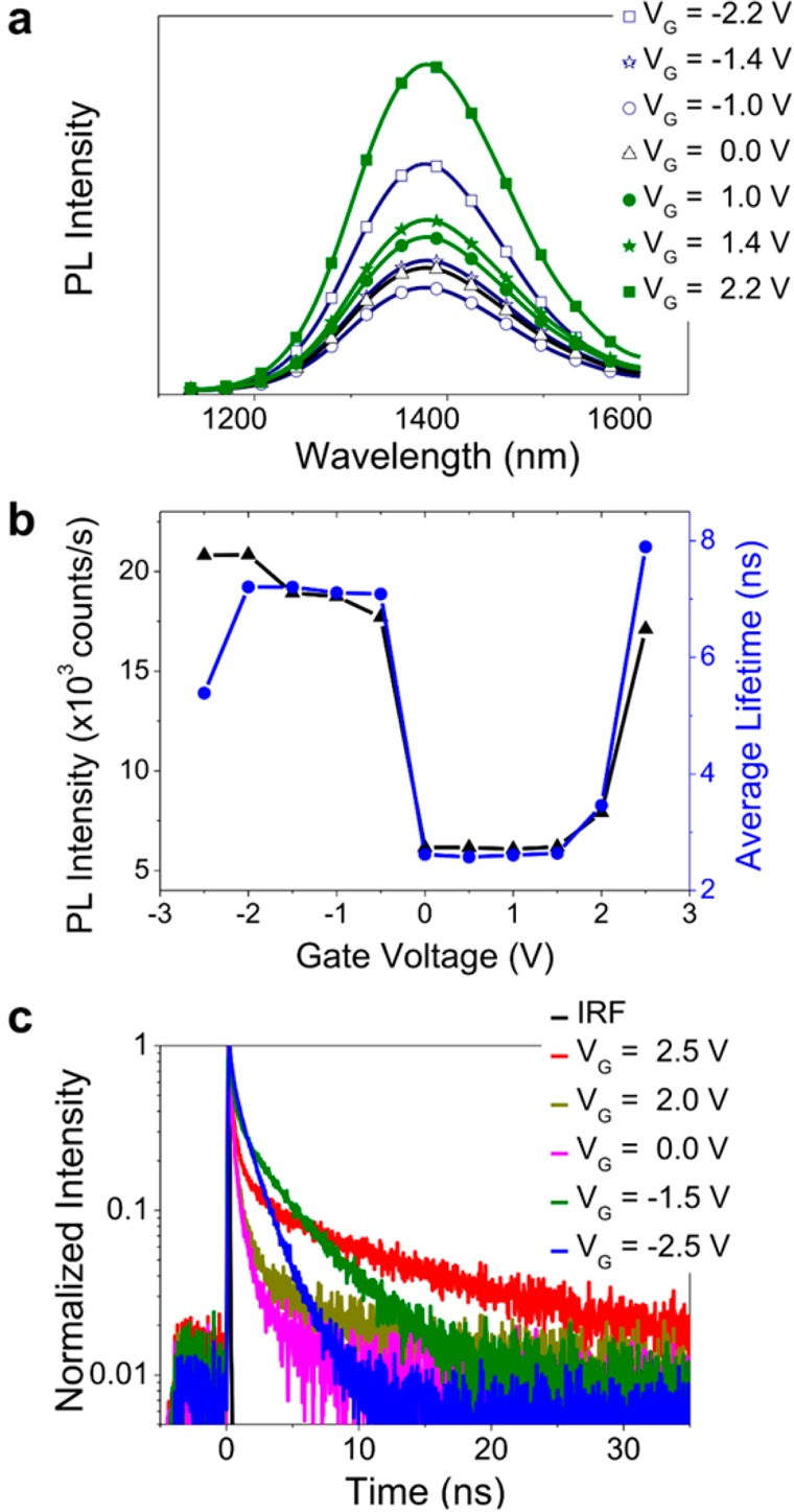
(a) PL spectra, (b) integrated PL intensity (black triangles) and average emission lifetime (blue circles) at different doping levels, and (c) corresponding normalized PL decays of PbS 2 QDs (IRF = instrument response function).
With the aim to understand this effect we performed PL lifetime measurements for different applied gate voltages and thus levels of electron and hole doping of QD films. Note that this is essentially an electrochemical doping experiment with the source/drain electrodes acting as the working electrode and the gate as the counter electrode. In order to monitor the conductivity of the QD film we applied a small source-drain voltage of −10 mV. VDS is kept very low so that the apparent onset of electron transport is not significantly shifted to more negative gate voltages. It also ensures that only one type of charge carrier is present and no electroluminescence occurs. The excitation power was kept low enough as to avoid multiexciton contributions (see Supporting Information I). Figure 4b presents PL intensity and PL average lifetime for PbS 2 quantum dots and the corresponding PL transients for selected gate voltages (Figure 4c) (see Supporting Information J for the definition of average lifetime and data for PbS 1 and PbS 3 QDs). The signal intensity follows the dependence of the average lifetime on gate voltage, that is, lifetime and intensity increase for hole and electron accumulation.
The observed increase in intensity for charge accumulation can be a sign of a larger number of QDs with high PL QY and/or higher PL QY of the particles that emit. Additional changes in the average decay lifetime imply a modification of the radiative and nonradiative recombination channels. At high doping levels, we can create large numbers of positive or negative excitons, that is, trions. Trions are generated when an imbalance of charge carriers occurs due to surface trapping or electron/hole accumulation.35−40 Trion lifetimes are usually much shorter than exciton lifetimes due to the fast Auger decay rate (nonradiative losses) and higher probability of radiative decay. This in turn may lead to a higher PL QY of trions compared to excitons with fast nonradiative decay channels although most reports consider trions as “dark” or “gray” emitting species in terms of emission efficiencies.36,38,39 In our case, a larger number of trions explains the variations of both lifetime and PL intensity with doping that cannot be explained by simple compensation of trap states.
Analysis of the PL intensity decays sheds light on the observed trends (Figure 4c). For initial conditions and positive gate voltages (0 V < VG < 2 V, no mobile electrons and no significant changes of PL intensity) the PL decay is dominated by a fast decay component. Taking into account the low PL quantum yields (∼0.05–0.07%) and long exciton radiative lifetimes of all three PbS QD films (assuming they are the same as in solutions, i.e. ∼ 1–3 μs, see Supporting Information K), this component represents fast nonradiative decay channels in the QDs. When VG > 2 or 0 V > VG > −2 V an additional slow decay component emerges, leading to an effective increase of the arrival time of the detected photons. More importantly, the decay slopes of the long-lived components are increasing, thus, the associated time constant decreases. This becomes especially clear for VG = −2.5 V (see Figure 4b,c and Supporting Information J, Figure S8).
In order to investigate these trends quantitatively, we used nonlinear transient analysis to separate the slow decay components from the fast components similar to an approach used by Saba et al.37 The PL decay curve at VG = 0 V was subtracted from the other transients (see Supporting Information Figure S10a–c). The resulting signal can be easily fitted with a monoexponential decay function giving a lifetime that corresponds directly to the component that only appears for high doping levels (see Supporting Information, Figure S10d–f). As expected from the observed increase of the average lifetime in Figure 4b, most of the obtained lifetime values for the slow decay components are higher than the initial average lifetime at VG = 0 V (1–12 ns versus 2–3 ns). A second calculation method using a triexponential fit, taking into account the instrument response function (IRF) (see Supporting Information L), was used to estimate the missing data in the range 0 V < VG < 2 V and to check the reliability of the fitting methods. Both methods gave an excellent correlation of the obtained values and low fit residuals (Supporting Information Figure S10d–f and S11). For all QDs, the values of the decay lifetime for hole and electron doping are found to be different. That is, for positive voltages >2 V (electron accumulation) the lifetime is longer than for negative voltages <0 V (hole accumulation). This leads to the conclusion that positive and negative trions may have different lifetimes.
Unfortunately, only a few papers compare the lifetimes of positive and negative trions and the issue remains unclear.36−38,40 It is believed that mirror symmetry between the valence and conduction bands for PbS will cause similar trion lifetimes for both signs. As for the absolute values it is common to estimate the trion lifetimes from the biexciton Auger-decay lifetimes.38 For example, for the PbS QDs of the same size used in this study but with oleic acid ligands a biexciton Auger-decay lifetime of less than 100 ps was measured by Stewart et al.,41 which would lead to a trion lifetime of a few hundred picoseconds. This is one order of magnitude lower than the trion lifetimes of a few nanoseconds that we observe for our QD films. Differences between the density of states effective mass of holes and electrons (for PbS: mh*/me ≈ 0.6342), charged surface ligands, and strong local fields due to the electrolyte-gating could introduce asymmetric localization/delocalization of electron and holes in quantum dot thin films and thus change the absolute values and the ratio of positive and negative trion lifetimes substantially.
Apart from the variation of the average lifetime due to trion emission, the intensity enhancement is still unclear. Using the amplitudes of the exponents from the triexponential fit we can renormalize these values in order to represent the fraction of the emitting species with a sum of fast and slow components (see Supporting Information L for details). According to this procedure only 1–3% of the QDs are responsible for the slow decay components at VG = 0 V, whereas for higher voltages this fraction drastically increases up to 35% (Supporting Information Figure S10g–i). Taking into account that fractions of the fast components decrease only slightly and their lifetime is fixed, we can conclude that the observed intensity variation in Figure 4a is due to the modulation of the number of emitting quantum dots associated with the slow decaying component. Following our previous conclusion, that this emission is trion-related and the total intensity of the emission increases, we can state that trion emission is higher than emission from particles associated with the fast decaying component. According to these considerations, 97–99% of the initial QDs (at VG = 0 V) are inefficient emitters.
One of the probable reasons for the surprising transformation of dark into bright QDs at high doping levels could be the decrease of the nonradiative losses via electron and hole trap states. As recently discussed, recombination centers can be efficiently activated or deactivated by the variation of the relative position of the Fermi level.39 This effect is also well-known from the operation of FETs and is reflected in the threshold voltage, at which trap states are filled and charge carriers become mobile.43 The appearance of hole and electron midgap states was considered to be caused by defects, ligands, and stoichiometry variations.44−47 For our ensemble measurements, we can expect the presence of two subgroups of QDs with excess of either electron or hole trap states. If those traps contribute equally to the same QD, compensation may occur, leading to the effective deactivation of both trap states and thus a higher ratio of radiative to nonradiative decay rates.
Figure 5 summarizes our model for the observed intensity and lifetime variations for three typical conditions of charge accumulation in QDs. Here, the first and the last column correspond to the electron and hole accumulation regimes, while the middle column corresponds to the initial conditions. Recombination channels within the QDs with either predominant electron (“blue” QDs) or hole (“red” QDs) traps are depicted together with QDs where compensation occurs (“green” QDs). Depending on the applied gate voltage, the Fermi level (EF) is shifted with respect to their energetic position (Et– and Et+ for electrons and holes, respectively), leading to the activation or deactivation of the traps. For initial conditions (middle column, 0 V < VG < 2 V, no mobile carriers), exciton emission is represented as a sum of radiative γrX0 and nonradiative γnrX0 decay rates for all QDs. The latter corresponds to the intrinsic (not related to traps) exciton losses via quenching or dissociation. However, most of the QDs (97–99%) are dark, because they are dominated by nonradiative transitions with a fast decay rate (γnr). For the electron accumulation regime (left column, VG > 2 V), the shift of the Fermi level leads to the deactivation of electron traps in numerous QDs, converting them into QDs with negative trion emission with corresponding radiative (γrX–) and nonradiative (γnrX–) decay rates. This manifests itself in the modified lifetime and increased intensity of the slow decay component (Figure 4b,c, and Supporting Information Figure S8). It is worth noting that the shift of the Fermi level also leads to the transformation of previously bright QDs (“green” at 0 V < VG < 2 V) into QDs with hole traps (“red”), while QDs with hole traps remain unaffected. The same situation occurs for the hole accumulation regime (last column Figure 5, VG < 0 V). Now light emission is dominated by the radiative recombination of positive trions (with radiative γrX+ and nonradiative γnrX+ decay rates). Comparing the expected temporal response of the QDs governed by the above-mentioned decay channels with nonlinear PL transients, we can again justify the assignment of the slow decay component to trion emission (see Supporting Information M for details). The effective deactivation of the traps via carrier density can also be mediated via excitation/pumping rate with a laser, even without electrical charge injection (see Supporting Information N, Figure S12). Note that midbandgap states may also be radiative.44,46 However, due to the limitation of our detectors photons with wavelengths above 1600 nm were not detected and thus corresponding transitions are considered as nonradiative in our model.
Figure 5.
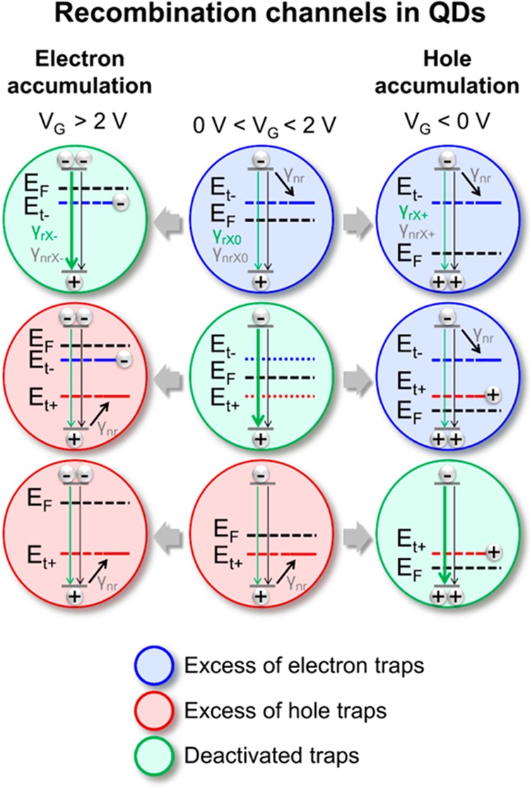
Scheme of recombination channels in QDs. Middle column, initial conditions (0 V < VG < 2 V); left column, electron accumulation (VG > 2 V); and right column, hole accumulation (VG < 0 V). The colors of the schematic QDs indicate an excess of electron (blue) or hole (red) trap states (Et– and Et+) with an effective trapping rate γnr. The QDs with deactivated trap states are shown in green. The relative position of the Fermi level (EF) is defined by the gate voltage and turns numerous nonemissive QDs into QDs with more efficient trion emission (with radiative γrX–, γrX+ and nonradiative γnrX–, γnrX+ decay rates).
According to the proposed model, the increased charge carrier density has a two-fold effect. First, it leads to dominant trion emission. And second, a large number of QDs with fast nonradiative losses becomes luminescent, effectively increasing the overall emission efficiency. The latter is probably the main reason for the observed increase of EQE in QD LEFETs at higher current densities as shown in Figure 3b despite the low PL efficiencies of the ligand-exchanged films. Although deactivation of trap states might describe improved EQE, the introduction of trions into the model is necessary to explain different emission lifetimes for positive and negative charge accumulation, as shown in Supporting Information Figure S10.
In summary, we demonstrated the first ambipolar, light-emitting field-effect transistor based on quantum dots. We used electrolyte-gating in order to achieve ambipolar transport in ligand-exchanged PbS quantum dot thin films with high current densities. This resulted in near-infrared emission from a confined zone, whose position within the channel and intensity could be controlled by the applied voltages. These quantum dot LEFETs finally complete the series of light-emitting transistors from zero-dimensional to bulk semiconductors. Further, electrolyte-gated PbS QD FETs enabled the investigation of electron–hole recombination and emission in QD solids at high charge carrier concentrations. We found that emission was initially limited by nonradiative decay channels due to charge carrier traps. Electron and hole accumulation lead to increased trion emission and higher PL quantum yields, which also explains the increase of external quantum efficiency in LEFETs at higher current densities. Our results suggest that high carrier densities are not always detrimental to device performance but can indeed improve it. These findings have implications for solar cells and light-emitting devices based on QD solids, whose performance strongly depends on carrier density and recombination dynamics.
Acknowledgments
This research was financially supported by the Deutsche Forschungsgemeinschaft (DFG, ZA 638/2). J.S. gratefully acknowledges the Graduate School “Advanced Materials and Processes” (GS-AMP) and the Graduate School in “Advanced Optical Technologies” (SAOT) within the framework of the German Excellence Initiative. Y.Z. acknowledges funding by the European Research Council under the European Union’s Seventh Framework Programme (FP/2007-2013)/ERC Grant 306298 (EN-LUMINATE). J.Z. also thanks the Alfried Krupp von Bohlen und Halbach-Stiftung and the Cluster of Excellence “Engineering of Advanced Materials” (EXC 315) for general support. The authors thank B. Winter for help with TEM measurements, K. Ludwig and S. B. Grimm for help with device fabrication. J.S. thanks the Sargent group (University of Toronto) for the opportunity to learn about basic QD thin film device fabrication.
Supporting Information Available
Methods: Synthesis and characterization of PbS QDs, fabrication and characterization of LEFETs, and measurement of PL spectra of PbS QD solutions and films. Additional data and analysis: effect of PbS QD film annealing, output and transfer characteristics of electrolyte-gated FETs, movie of the moving emission zone in an electrolyte-gated PbS QD light-emitting FET, position and width of PbS QD emission zone at different gate voltages, FETs with HfOx dielectric and top gate, PbS FETs fabricated with QDs synthesized with PbCl2 and sulfur, gate voltage dependence of PL intensity, calculation of excitation density for lifetime measurements, variation of intensity and PL decay for high electron and hole accumulation levels, radiative exciton lifetime, transient photoluminescence analysis, estimation of PL transients for high electron and hole accumulation levels, and influence of the excitation power density on the PL decay. This material is available free of charge via the Internet at http://pubs.acs.org.
The authors declare no competing financial interest.
Supplementary Material
References
- Gao J.; Perkins C. L.; Luther J. M.; Hanna M. C.; Chen H.-Y.; Semonin O. E.; Nozik A. J.; Ellingson R. J.; Beard M. C. Nano Lett. 2011, 11, 3263–3266. [DOI] [PubMed] [Google Scholar]
- Ip A. H.; Thon S. M.; Hoogland S.; Voznyy O.; Zhitomirsky D.; Debnath R.; Levina L.; Rollny L. R.; Carey G. H.; Fischer A.; Kemp K. W.; Kramer I. J.; Ning Z.; Labelle A. J.; Chou K. W.; Amassian A.; Sargent E. H. Nat. Nanotechnol. 2012, 7, 577–582. [DOI] [PubMed] [Google Scholar]
- Chuang C.-H. M.; Brown P. R.; Bulović V.; Bawendi M. G. Nat. Mater. 2014, 13, 796–801. [DOI] [PMC free article] [PubMed] [Google Scholar]
- Rauch T.; Boberl M.; Tedde S. F.; Furst J.; Kovalenko M. V.; Hesser G.; Lemmer U.; Heiss W.; Hayden O. Nat. Photonics 2009, 3, 332–336. [Google Scholar]
- Clifford J. P.; Konstantatos G.; Johnston K. W.; Hoogland S.; Levina L.; Sargent E. H. Nat. Nanotechnol. 2009, 4, 40–44. [DOI] [PubMed] [Google Scholar]
- Sukhovatkin V.; Hinds S.; Brzozowski L.; Sargent E. H. Science 2009, 324, 1542–1544. [DOI] [PubMed] [Google Scholar]
- Talapin D. V.; Murray C. B. Science 2005, 310, 86–89. [DOI] [PubMed] [Google Scholar]
- Liu Y.; Tolentino J.; Gibbs M.; Ihly R.; Perkins C. L.; Liu Y.; Crawford N.; Hemminger J. C.; Law M. Nano Lett. 2013, 13, 1578–1587. [DOI] [PubMed] [Google Scholar]
- Kang M. S.; Lee J.; Norris D. J.; Frisbie C. D. Nano Lett. 2009, 9, 3848–3852. [DOI] [PubMed] [Google Scholar]
- Oh S. J.; Berry N. E.; Choi J.-H.; Gaulding E. A.; Lin H.; Paik T.; Diroll B. T.; Muramoto S.; Murray C. B.; Kagan C. R. Nano Lett. 2014, 14, 1559–1566. [DOI] [PubMed] [Google Scholar]
- Bisri S. Z.; Piliego C.; Yarema M.; Heiss W.; Loi M. A. Adv. Mater. 2013, 25, 4309–4314. [DOI] [PubMed] [Google Scholar]
- Colvin V. L.; Schlamp M. C.; Alivisatos A. P. Nature 1994, 370, 354–357. [Google Scholar]
- Coe S.; Woo W.-K.; Bawendi M.; Bulović V. Nature 2002, 420, 800–803. [DOI] [PubMed] [Google Scholar]
- Cho K.-S.; Lee E. K.; Joo W.-J.; Jang E.; Kim T.-H.; Lee S. J.; Kwon S.-J.; Han J. Y.; Kim B.-K.; Choi B. L.; Kim J. M. Nat. Photonics 2009, 3, 341–345. [Google Scholar]
- Sun L.; Choi J. J.; Stachnik D.; Bartnik A. C.; Hyun B.-R.; Malliaras G. G.; Hanrath T.; Wise F. W. Nat. Nanotechnol. 2012, 7, 369–373. [DOI] [PubMed] [Google Scholar]
- Zaumseil J.; Sirringhaus H. Chem. Rev. 2007, 107, 1296–1323. [DOI] [PubMed] [Google Scholar]
- Zaumseil J.; Donley C. L.; Kim J.-S.; Friend R. H.; Sirringhaus H. Adv. Mater. 2006, 18, 2708–2712. [Google Scholar]
- Takahashi T.; Takenobu T.; Takeya J.; Iwasa Y. Adv. Funct. Mater. 2007, 17, 1623–1628. [Google Scholar]
- Zhang Y. J.; Oka T.; Suzuki R.; Ye J. T.; Iwasa Y. Science 2014, 344, 725–728. [DOI] [PubMed] [Google Scholar]
- Sundaram R. S.; Engel M.; Lombardo A.; Krupke R.; Ferrari A. C.; Avouris P.; Steiner M. Nano Lett. 2013, 13, 1416–1421. [DOI] [PubMed] [Google Scholar]
- Freitag M.; Chen J.; Tersoff J.; Tsang J. C.; Fu Q.; Liu J.; Avouris P. Phys. Rev. Lett. 2004, 93, 076803. [DOI] [PubMed] [Google Scholar]
- Jakubka F.; Backes C.; Gannott F.; Mundloch U.; Hauke F.; Hirsch A.; Zaumseil J. ACS Nano 2013, 7, 7428–7435. [DOI] [PubMed] [Google Scholar]
- Hines M. A.; Scholes G. D. Adv. Mater. 2003, 15, 1844–1849. [Google Scholar]
- Steckel J. S.; Coe-Sullivan S.; Bulović V.; Bawendi M. G. Adv. Mater. 2003, 15, 1862–1866. [Google Scholar]
- Kang I.; Wise F. W. J. Opt. Soc. Am. B 1997, 14, 1632–1646. [Google Scholar]
- Lee J.; Panzer M. J.; He Y.; Lodge T. P.; Frisbie C. D. J. Am. Chem. Soc. 2007, 129, 4532–4533. [DOI] [PubMed] [Google Scholar]
- Thiemann S.; Gruber M.; Lokteva I.; Hirschmann J.; Halik M.; Zaumseil J. ACS Appl. Mater. Interfaces 2013, 5, 1656–1662. [DOI] [PubMed] [Google Scholar]
- Liu Y.; Gibbs M.; Puthussery J.; Gaik S.; Ihly R.; Hillhouse H. W.; Law M. Nano Lett. 2010, 10, 1960–1969. [DOI] [PubMed] [Google Scholar]
- Luther J. M.; Law M.; Song Q.; Perkins C. L.; Beard M. C.; Nozik A. J. ACS Nano 2008, 2, 271–280. [DOI] [PubMed] [Google Scholar]
- Thiemann S.; Sachnov S.; Porscha S.; Wasserscheid P.; Zaumseil J. J. Phys. Chem. C 2012, 116, 13536–13544. [Google Scholar]
- Weidman M. C.; Beck M. E.; Hoffman R. S.; Prins F.; Tisdale W. A. ACS Nano 2014, 8, 6363–6371. [DOI] [PubMed] [Google Scholar]
- Kovalenko M. V.; Bodnarchuk M. I.; Zaumseil J.; Lee J.-S.; Talapin D. V. J. Am. Chem. Soc. 2010, 132, 10085–10092. [DOI] [PubMed] [Google Scholar]
- van Reenen S.; Vitorino M. V.; Meskers S. C. J.; Janssen R. A. J.; Kemerink M. Phys. Rev. B 2014, 89, 205206. [Google Scholar]
- Reich K. V.; Chen T.; Efros A. L.; Shklovskii B. I. Phys. Rev. B 2013, 88, 245311. [Google Scholar]
- Jakubka F.; Grimm S. B.; Zakharko Y.; Gannott F.; Zaumseil J. ACS Nano 2014, 8, 8477–8486. [DOI] [PubMed] [Google Scholar]
- Park Y.-S.; Bae W. K.; Pietryga J. M.; Klimov V. I. ACS Nano 2014, 8, 7288–7296. [DOI] [PubMed] [Google Scholar]
- Saba M.; Aresti M.; Quochi F.; Marceddu M.; Loi M. A.; Huang J.; Talapin D. V.; Mura A.; Bongiovanni G. ACS Nano 2013, 7, 229–238. [DOI] [PubMed] [Google Scholar]
- Jha P. P.; Guyot-Sionnest P. ACS Nano 2009, 3, 1011–1015. [DOI] [PubMed] [Google Scholar]
- Galland C.; Ghosh Y.; Steinbruck A.; Sykora M.; Hollingsworth J. A.; Klimov V. I.; Htoon H. Nature 2011, 479, 203–207. [DOI] [PMC free article] [PubMed] [Google Scholar]
- Qin W.; Liu H.; Guyot-Sionnest P. ACS Nano 2014, 8, 283–291. [DOI] [PubMed] [Google Scholar]
- Stewart J. T.; Padilha L. A.; Qazilbash M. M.; Pietryga J. M.; Midgett A. G.; Luther J. M.; Beard M. C.; Nozik A. J.; Klimov V. I. Nano Lett. 2012, 12, 622–628. [DOI] [PubMed] [Google Scholar]
- Lide D. R.CRC Handbook of Chemistry and Physics; CRC Press: Boca Raton, FL, 2010; Vol. 90. [Google Scholar]
- Kang M. S.; Sahu A.; Norris D. J.; Frisbie C. D. Nano Lett. 2010, 10, 3727–3732. [DOI] [PubMed] [Google Scholar]
- Brovelli S.; Galland C.; Viswanatha R.; Klimov V. I. Nano Lett. 2012, 12, 4372–4379. [DOI] [PubMed] [Google Scholar]
- Kim D.; Kim D.-H.; Lee J.-H.; Grossman J. C. Phys. Rev. Lett. 2013, 110, 196802. [DOI] [PubMed] [Google Scholar]
- Mooney J.; Krause M. M.; Saari J. I.; Kambhampati P. J. Chem. Phys. 2013, 138, 204705. [DOI] [PubMed] [Google Scholar]
- Peterson M. D.; Cass L. C.; Harris R. D.; Edme K.; Sung K.; Weiss E. A. Annu. Rev. Phys. Chem. 2014, 65, 317–339. [DOI] [PubMed] [Google Scholar]
Associated Data
This section collects any data citations, data availability statements, or supplementary materials included in this article.


