Abstract
Semiconducting two-dimensional transition metal dichalcogenides are emerging as top candidates for post-silicon electronics. While most of them exhibit isotropic behaviour, lowering the lattice symmetry could induce anisotropic properties, which are both scientifically interesting and potentially useful. Here we present atomically thin rhenium disulfide (ReS2) flakes with unique distorted 1T structure, which exhibit in-plane anisotropic properties. We fabricated monolayer and few-layer ReS2 field-effect transistors, which exhibit competitive performance with large current on/off ratios (∼107) and low subthreshold swings (100 mV per decade). The observed anisotropic ratio along two principle axes reaches 3.1, which is the highest among all known two-dimensional semiconducting materials. Furthermore, we successfully demonstrated an integrated digital inverter with good performance by utilizing two ReS2 anisotropic field-effect transistors, suggesting the promising implementation of large-scale two-dimensional logic circuits. Our results underscore the unique properties of two-dimensional semiconducting materials with low crystal symmetry for future electronic applications.
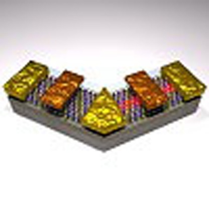 Many two-dimensional materials exhibit isotropic properties, but anisotropy can extend the functionality of future devices. Here, the authors fabricate field-effect transistors from single and few-layer rhenium disulfide and observe an anisotropic ratio of three to one along the two principle axes
The scaling down of conventional metal-oxide-semiconductor FETs is approaching the limit of miniaturization due to severe short-channel effects1. One approach to solve this problem is searching for atomically thin semiconductors, such as semiconducting two-dimensional (2D) materials2,3,4,5,6. Among the potential candidates, the family of transition metal dichalcogenides (TMDs)7,8 (MX2, where M denotes a transition metal and X denotes a chalcogen) has attracted the most attention due to both its rich physics and tremendous potential for application. They are expected to exhibit a wide range of electronic structures and exotic transport properties arising from the various electron configurations of transition metals, such as superconductivity9,10,11, half-metallic magnetism12 and charge density waves13,14,15.
Lattice structure and symmetry are vital in determining materials' fundamental properties. Most studied 2D TMDs exhibit isotropic behaviour due to high lattice symmetry; however, lowering the symmetry in TMDs could induce interesting anisotropic properties of both scientific and technologic importance. For example, in WTe2, which is a semi-metallic TMD with a distorted lattice structure, a large non-saturating magnetoresistance effect along a principle axis (the direction of W chain formation) has been recently reported and has attracted considerable attention16. In contrast, semiconducting 2D TMDs with low symmetry have remained unexplored.
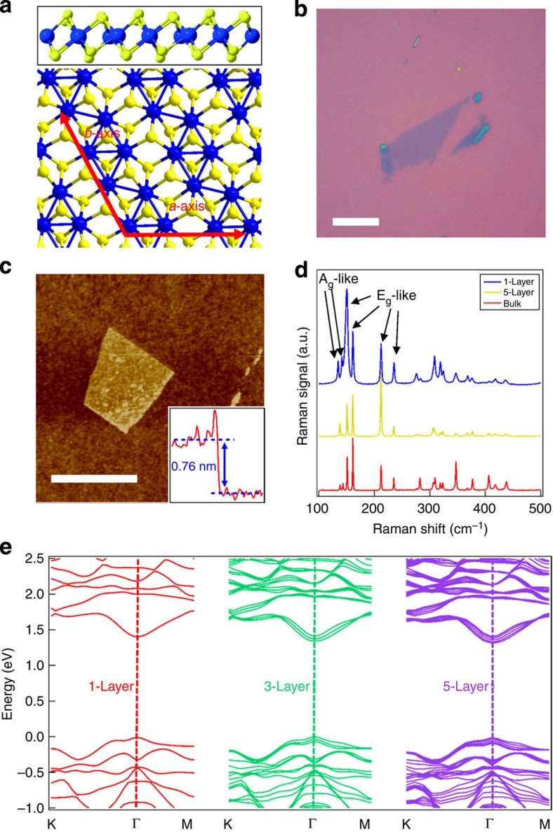
As the last stable element discovered in nature, the transition metal rhenium (Re) exhibits a wide range of oxidation states and crucial applications, such as superalloys and catalytic reforming. Its sulfide rhenium disulfide (ReS2) is a semiconducting TMD that was recently discovered to have weak interlayer coupling and a unique distorted 1T structure17. As shown by the side view and top view of the monolayer ReS2 crystal structure in Fig. 1a, it consists of two hexagonal planes of S atoms (yellow) and an intercalated hexagonal plane of Re atoms (blue) bound with S atoms forming chains of parallelogram-shaped Re4 clusters. As highlighted by the red arrows in the top view, there are two principle axes, the b and a axes, which correspond to the shortest and second-shortest axes in the basal plane. They are 61.03° or 118.97° apart, and the b axis corresponds to the direction of the Re–Re atomic chain formed. Thus, ReS2 offers an ideal material candidate for studying semiconducting 2D TMDs with low symmetry.
Figure 1. Characterization and band structure of thin-layer ReS2.
(a) Crystal structure of monolayer ReS2 with a side view in the top panel and a top view in the bottom panel. Both directions of a and b axes are denoted by red arrows. (b) Optical image of a monolayer ReS2 flake. Scale bar, 10 μm. (c) AFM image of a monolayer ReS2 flake. Scale bar, 1 μm. Inset: height profile along the blue line indicating a single layer. (d) Micro Raman experimental results performed on monolayer, five-layer and bulk ReS2. Six labelled Raman modes include two low frequency Ag-like modes corresponding to the out-of-plane vibrations of Re atoms and four Eg-like modes corresponding to the in-plane vibrations of Re atoms. The rest 12 higher frequency Raman modes are vibrations mainly from lighter S atoms. (e) Band structure of monolayer, trilayer and five-layer ReS2 by ab initio calculations indicating band gaps of 1.44, 1.40 and 1.35 eV, respectively. AFM, atomic force microscope.
In this work, we systematically investigate the in-plane anisotropic properties of atomically thin ReS2. In addition to highly competitive FET performance, we also observe a large anisotropic ratio along its two principle axes, which is the highest among all experimentally investigated 2D layered materials. We also successfully demonstrate a digital inverter with good performance by integrating two anisotropic ReS2 FET devices. Our results suggest that the lattice orientation can be used as an alternative design variable to tune device properties and optimize circuit performance in future 2D integrated circuits based on the anisotropic semiconducting materials.
Results
Material characterizations and ab initio calculations
Figure 1b,c shows typical optical microscopy and atomic force microscope images of a monolayer ReS2 film (see Methods for the material details), respectively. The inset of Fig. 1c shows that the thickness of the monolayer film is ∼0.8 nm. In this study, we focus on monolayer and few-layer ReS2, with thicknesses ranging from 0.8 to 5 nm (1–7 layers with interlayer spacing of ∼0.7 nm). Micro Raman scattering experiments were performed on monolayer, five-layer and bulk ReS2. Due to the low symmetry of ReS2, 18 Raman modes were observed as shown in Fig. 1d. The peak positions of our three samples are close to each other, same to the reported results17. In Fig. 1d, we labelled two low frequency Ag-like modes (located at 136.8 and 144.5 cm−1) corresponding to the out-of-plane vibrations of Re atoms and four Eg-like modes (located at 153.6, 163.4, 218.2 and 238.1 cm−1) corresponding to the in-plane vibrations of Re atoms. The rest 12 higher frequency Raman modes are vibrations mainly from lighter S atoms18. The peak intensity ratio could be dependent on the polarization due to the low lattice symmetry19. The band structures of monolayer, trilayer and five-layer ReS2 calculated by an ab initio method are shown in Fig. 1e, indicating the nature of a direct band gap semiconductor without the indirect-to-direct band gap transition observed in other TMDs3. The overall band topology does not significantly change, with only a minor band gap shortening from monolayer (1.44 eV), trilayer (1.4 eV) to five-layer (1.35 eV).
FET performances
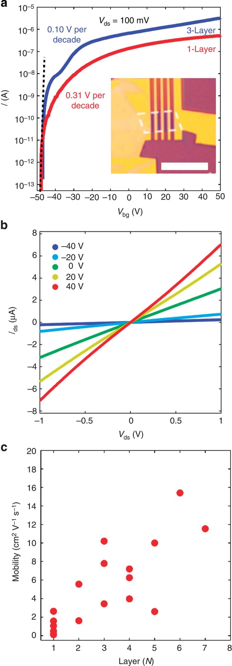
We first examine the device performances of monolayer and few-layer ReS2 FET devices (see Supplementary Note 1 for details). The inset of Fig. 2a presents the optical image of a typical monolayer device. The FET transfer curve was obtained by monitoring the source–drain current Ids while sweeping the back gate voltage Vbg. A fixed 100-mV source–drain bias voltage Vsd was applied across the channel during all of the measurements. We first measured a couple of monolayer ReS2 devices, all of which behaved as excellent n-type FET devices with the back gate swept between −50 and +50 V. As shown in Fig. 2a, the current on/off ratio reached 107, which meets the requirement of many applications, such as digital logic computation. When the back gate voltage reached +50 V, the Ids approached saturation. Few-layer ReS2 transistor devices, ranging from bilayer to seven-layer, were studied as well. Similar n-type FET behaviour but a slightly larger on/off ratio was observed. The results from a trilayer device with the same back gate sweep range are shown in Fig. 2a for comparison. We note that all of the above measurements were carried out under vacuum (∼10−5 mbar) at room temperature, and ambipolar behaviour can be observed by introducing the ionic liquid gating technique (see Supplementary Note 2 for details). On the basis of the transfer curves, we can also measure the subthreshold swing. For the monolayer ReS2 FET device shown in Fig. 2a, the subthreshold swing is ∼310 mV per decade. The subthreshold swing becomes steeper for thicker flakes, reaching ∼100 mV per decade for the trilayer device shown in the same figure. The measured subthreshold swing values approach those measured in top-gated MoS2 transistors7 and outperform black phosphorus devices5. This can be further improved by increasing the gate capacitance after introducing thinner high-κ dielectric materials.
Figure 2. ReS2 field-effect transistor devices.
(a) Transfer curves of monolayer (red) and trilayer (blue) ReS2 FET devices. Vds is fixed to 100 mV. The on/off ratio is ∼107 for the monolayer device and 107 for the seven-layer device. The subthreshold swings are 310 mV per decade (monolayer) and 100 mV per decade (trilayer), respectively. Inset: optical image of a typical monolayer ReS2 FET device. Scale bar, 5 μm. (b) Ids–Vds curves of a monolayer ReS2 FET at different Vbg, with linear dependence indicating the ohmic contact. (c) The dependence of device mobility on the number of layers. In general, the mobility increases monotonically with the number of layers with some scattering.
The monolayer and few-layer ReS2 FET devices (with Ti/Au electrodes) have also shown good contact behaviour. As shown in Fig. 2b, for a typical monolayer device, the source–drain current Ids varies linearly with the bias Vds in the ±1 V range at different back gate voltages (Vbg=−40, −20, 0, 20 and 40 V, respectively), indicating ohmic contact behaviour in the n-doped regime under consideration (see Supplementary Note 3 for more details).
We further extracted the mobility of all of the FET devices we measured and studied its dependence on the number of layers of the ReS2. The mobility was determined by taking the steepest slope in the two-terminal Ids–Vbg curves. The results for 17 devices (from monolayer to seven-layer) are plotted in Fig. 2c. Similar to the reported results based on MoS2 thin flakes20,21, the device mobility generally increases with an increasing number of layers, implying that the electrons likely independently transport through different layers in thin ReS2 flakes. The mobility of a monolayer device varies between 0.1 and 2.6 cm2 V−1 s−1, and the highest mobility value obtained is 15.4 cm2 V−1 s−1 for a six-layer device. These values were measured without any material treatment or device optimization. With further improvement in crystal quality, post-fabrication treatment22 and dielectric engineering7,22, considerable enhancement of mobility to approach application requirements should be expected. Here the scattering of mobility values for flakes with the same number of layers could be induced by device quality variations or the anisotropic property, as will be discussed below.
Anisotropic properties of ReS2
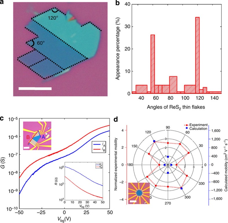
We now focus on the in-plane anisotropic properties of monolayer and few-layer ReS2 flakes induced by low lattice symmetry. As described in Fig. 1a, the a and b axes are the two directions with the shortest axes in the basal plane, thus differentiating them from other lattice orientations. Such a feature is often associated with the in-plane anisotropic properties of structural stiffness and electronic transport. Interestingly, during our experiments, exfoliated thin ReS2 flakes commonly appear in a quadrilateral shape with inner angles of ∼60° or 120°, as shown by a typical flake in Fig. 3a. Further results of all inner angles measured on over 20 thin flakes is shown in Fig. 3b, with >60% of the specimens showing these two angles. The inner angles of 60° and 120° match the angles between the a and b axes (118.97° or 61.03°) with high accuracy. This can be readily explained by the fact that the breaking strength is the weakest along these two axes, which are the two most strongly bonded orientations17,23, and suggests that two sides of the quadrilateral shape with 60° or 120° inner angles correspond to the a and b axes, respectively.
Figure 3. Anisotropic properties of ReS2.
(a) Optical image of a typical thin ReS2 flake with a quadrilateral shape. Scale bar, 5 μm. (b) The statistics of inner angles for over 20 thin ReS2 flakes, showing the greatest prevalence for 60° and 120°. (c) Transfer curves of anisotropic ReS2 FETs along two sides (A and B direction) of a quadrilateral-shaped five-layer flake (with an inner angle of 60° or 120°). Top inset: optical image of the devices. Scale bar, 10 μm. Low inset: the 4-probe resistance of the same devices with Vbg varying between 0 and 60 V. (d) Normalized field-effect mobility of a six-layer device along 12 directions evenly spaced at 30° apart plotted in polar coordinates (red dots with left axis). The direction with the lowest mobility was set to be the 0° (or 180°) reference. The optical image of the device is shown in the inset. The calculated mobility of monolayer ReS2 along three orientations (a axis, b axis and perpendicular to the a axis) is plotted in the same graph (blue dots with right axis) for comparison. The lowest mobility (a axis) direction was set to be the 0° (or 180°) reference as well.
The in-plane stiffness anisotropy-induced quadrilateral shape makes it feasible to determine the two axes of ReS2 flakes via convenient transport measurements instead of other highly sophisticated tools, such as scanning tunnelling microscopy. Early studies on bulk materials reported that the b axis is more conductive than other crystalline orientations24,25. We then patterned the electrodes to be perpendicular to two sides (A and B directions) of a quadrilateral-shaped five-layer ReS2 with a 60° inner angle (as shown in the top inset of Fig. 3c). The transfer curves in two directions are shown in Fig. 3c, and anisotropic FET behaviour was observed. The B direction appears to be noticeably more conductive than the A direction, suggesting that the A and B directions correspond to the a and b axes, respectively. The conductance ratio of the two directions is gate dependent, with values of ∼8.2 when Vbg=−50 V and ∼2 when Vbg=50 V. To evaluate the influence of contact resistance, we performed four-terminal measurements (see Supplementary Note 3 for more details). The four-terminal results of the same device are shown in the lower inset of Fig. 3c, indicating that the anisotropy arises from the intrinsic properties of ReS2.
We further systematically studied the anisotropic properties of thin ReS2 flakes through angle-resolved transport measurement. As shown in the inset of Fig. 3d, a six-layer device was fabricated with 12 electrodes (5 nm Ti/50 nm Au) evenly spaced at 30° apart. We measured the transfer curves of each pair of diagonally positioned electrodes separated by 4.5 μm at 180° apart and extracted the renormalized field-effect mobility of each direction, with the results plotted in Fig. 3d (red dots) in polar coordinates. Measurements on each pair of electrodes lead to two data points that are 180° apart by swapping source–drain current directions. Here we define the direction with the lowest mobility to be the 0° (or 180°) reference. The field-effect mobility is highly angle dependent, with the largest value in the direction of 120° (or 300°), which is 60° from the direction with the lowest value. The anisotropic ratio of mobility μmax/μmin is ∼3.1, which is noticeably larger than that reported in other 2D anisotropic materials, such as 1.8 for thin-layer black phosphorus26.
To fully understand our observations, we calculated the effective mass and mobility of monolayer ReS2 along three crystalline orientations (a axis, b axis and perpendicular to the a axis) using an ab initio technique (see Supplementary Note 4 for details), with the results plotted in the same graph (blue dots with right axis). Here we set the direction with the lowest mobility (a axis) to be the 0° (or 180°) reference as well. By comparing with experimental data, the calculation results offer a qualitative explanation that for the device with polar coordinates, the direction of 0° (or 180°) approaches the a axis with the lowest mobility, 120° (or 300°) approaches the b axis with the highest mobility and 90° (or 270°) approaches the direction perpendicular to the a axis with a moderate mobility value between the two extremes. The quantitative discrepancies between the experimental and theoretical results imply that with continuous improvement of sample quality and material engineering, it is possible to achieve intrinsic properties that approach the real potential of ReS2 in high-performance device applications.
Digital inverter based on anisotropic ReS2 FETs
Anisotropic ReS2 FET devices with expected high mobility could have important applications in future nanoscale electronics, especially on 2D logic circuits27,28,29,30,31 with demanding requirements of scalability (<10 nm) and large-scale integration. In contrast to conventional complementary metal-oxide-semiconductor technologies, tailoring material properties and integrated circuit design variables (such as the channel width/length ratio)32 to optimize circuit performance on such a rigorous scale will remain a significant challenge. In this context, the lattice orientation could be used as an alternate design variable to tune device transport properties and optimize circuit performance in future 2D integrated circuits based on anisotropic semiconducting materials.
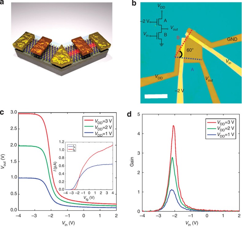
As a simple example, we successfully demonstrated a ReS2-based prototype logic device, a 2D digital inverter. As schematically shown in Fig. 4a, the inverter can be fabricated by combining two anisotropic ReS2 FETs along the a and b axes (with a Re atomic chain highlighted in red). In our experiment, a quadrilateral-shaped few-layer ReS2 flake with a 60° inner angle was selected to fabricate two FETs along two axes. HfO2 was then deposited with a thickness of 15 nm as the top dielectric, followed by the fabrication of two top-gate electrodes (30 nm Au). The optical image of a typical inverter device is shown in Fig. 4b. The transfer curves along the two directions are shown in the inset of Fig. 4c, which confirms the anisotropic behaviour and determines two axes as well. The circuit diagram is shown in the inset of Fig. 4b, where the top-gate voltage on the a axis is fixed at −2 V, the top-gate voltage on the b axis is the input voltage Vin and the middle shared electrode is the output voltage Vout. Figure 4c shows the voltage transfer characteristics with excellent logic-level conservation of our digital inverter, while Vin varies between −4 and 2 V for three different VDD values (3, 2 and 1 V with different colours). When Vin is above −1 V, Vout approaches 0 V, which denotes a digital 0. Similarly, when Vin is below −3 V, Vout approaches VDD, which denotes a digital 1. The output swing (defined as the largest difference of Vout) is close to the supply voltage VDD. As the most important parameter of a digital inverter, the gain is defined as |dVout/dVin|, which represents the sensitivity of Vout to the change in Vin. For this device, the gain reaches 4.4 when VDD=3 V (as shown in Fig. 4d). The gain that we obtained is clearly larger than the unity gain (gain=1), which is required in integrated circuits consisting of multiple cascaded inverters, such as ring oscillators, and is comparable to the MoS2 based inverters29,30.
Figure 4. Integrated digital inverters.
(a) A schematic showing the structure of an inverter combining two top-gated anisotropic ReS2 FETs. The left FET is along the a axis, and the right FET is along the b axis, where a Re atomic chain is highlighted in red. (b) Optical image of a typical inverter device. A quadrilateral-shaped few-layer ReS2 flake with a 60° inner angle was used to fabricate FETs along two axes covered by 15-nm-thick HfO2 as the top dielectric and two top-gate electrodes (30 nm Au). Scale bar, 10 μm. Inset: the circuit diagram of the inverter, where the top-gate voltage along the a axis is fixed at −2 V, the top-gate voltage along the b axis is the input voltage Vin and the middle shared electrode is the output voltage Vout. (c) Transfer characteristics of an inverter operated at VDD=1, 2 and 3 V. Inset: The transfer curves of two FETs with 100 mV Vds, confirming the anisotropic behavior. (d) The signal gain of the inverter extracted from c.
In conclusion, we have systematically studied the anisotropic properties of atomically thin ReS2, a semiconducting 2D TMD with a distorted 1T structure. We fabricated monolayer and few-layer ReS2 FET devices that exhibit competitive performance, including a high current on/off ratio (∼107) and a steep subthreshold swing (100 mV per decade) at room temperature. We also obtained an anisotropic ratio along the two principle axes of ReS2 that is the highest obtained for all experimentally studied 2D materials. Finally, we successfully demonstrated a digital inverter device by integrating two anisotropic ReS2 FET devices. Our results underscore the unique properties of semiconducting 2D materials with low symmetry, which can be exploited for novel applications in future electronics.
During the preparation of this manuscript, we became aware of another work studying the FET properties of few-layer ReS2 (ref. 33).
Methods
Materials and devices
Single crystals of ReS2 were grown by the same Br2-assisted chemical vapour transport method described in ref. 17. We used a standard mechanical exfoliation method to isolate monolayer and few-layer ReS2 films. The number of layers can be identified using the colour interference of a 285-nm-thick SiO2 wafer, and further confirmed by measuring the thickness of the flakes using a Bruker Multimode 8 atomic force microscope. Micro Raman scattering experiments (Horiba-JY T64000) were carried out under ambient conditions in the backscattering geometry. The incident laser wavelength was 514.5 nm, and the power was <1 mW to minimize laser heating. Due to the limitations of the spectrometer, we only measured Raman modes above 100 cm−1.
A conventional electron-beam lithography process (FEI F50 with Raith pattern generation system) followed by standard electron-beam evaporation of metal electrodes (typically 5 nm Ti/50 nm Au) was used to fabricate monolayer and few-layer ReS2 FET devices.
Ab initio calculations
Band structures for monolayer and few-layer ReS2 were calculated using the generalized gradient approximation Perdew–Burke–Ernzerhof function, as implemented in the VASP code (Vienna ab initio Simulation Package) within the density functional theory (DFT)34,35. Projector-augmented wave potentials were adopted36. The kinetic energy cutoff for the plane-wave basis set was 550 eV. The few-layer ReS2 was simulated with a vacuum layer of 15 Å in the interlayer direction to ensure negligible interaction between its periodic images. In the self-consistent calculations, the Brillouin zone integration was performed on uniform Monkhorst-Pack of 24 × 24 × 1 for few-layer ReS2 and 24 × 24 × 24 for bulk ReS2. The convergence criterion of self-consistent calculations for ionic relaxations was 10−5 eV between two consecutive steps. The internal coordinates and lattice constants were optimized until the atomic forces became <0.001 eV Å−1 and the pressures on the lattice unit cell became <0.5 kbr.
Author contributions
E.L. and Y.F. contributed equally to this work. F.M. and H.Y. conceived the project and designed the experiments. E.L., Y.F. and Y.W. carried out the device fabrication and electrical measurements. Y.F., H.L. and X.W. carried out the DFT calculations. W.Z. performed the Raman spectroscopy measurements and analysis. Y-S.H. and C-H.H. performed the ReS2 single crystal growth. Z.C., L.W. and A.L. performed the HfO2 growth. F.M., H.Y., B.W., E.L. and Y.F. performed the data analysis and interpretation. F.M., E.L., Y.F. and H.Y. co-wrote the paper, with all authors contributing to the discussion and preparation of the manuscript.
Additional information
How to cite this article: Liu, E. et al. Integrated digital inverters based on two-dimensional anisotropic ReS2 field-effect transistors. Nat. Commun. 6:6991 doi: 10.1038/ncomms7991 (2015).
Supplementary Material
Supplementary Figures 1-3, Supplementary Notes 1-4 and Supplementary References
Acknowledgments
We thank Chun Ning Lau, Marc Bockrath and J. Joshua Yang for stimulating discussions. This work was supported in part by the National Key Basic Research Program of China (2015CB921600, 2013CBA01603), the National Natural Science Foundation of China (11374142), the Natural Science Foundation of Jiangsu Province (BK20130544, BK20140017), the Specialized Research Fund for the Doctoral Program of Higher Education (20130091120040) and Fundamental Research Funds for the Central Universities. H.Y., H.Y.H. and Y.C. were supported by the Department of Energy, Office of Basic Energy Sciences, Division of Materials Sciences and Engineering, under contract DE-AC02-76SF00515.
References
- Ferain I., Colinge C. A. & Colinge J. Multigate transistors as the future of classical metal-oxide-semiconductor field-effect transistors. Nature 479, 310–316 (2011). [DOI] [PubMed] [Google Scholar]
- Nair R. R. et al. Fluorographene: a two-dimensional counterpart of teflon. Small 6, 2877–2884 (2010). [DOI] [PubMed] [Google Scholar]
- Mak K. F. et al. Atomically thin MoS2: a new direct-gap semiconductor. Phys. Rev. Lett. 105, 136805 (2010). [DOI] [PubMed] [Google Scholar]
- Wang Q. H. et al. Electronics and optoelectronics of two-dimensional transition metal dichalcogenides. Nat. Nanotechnol. 7, 699–712 (2012). [DOI] [PubMed] [Google Scholar]
- Li L. et al. Black phosphorus field-effect transistors. Nat. Nanotechnol. 9, 372–377 (2014). [DOI] [PubMed] [Google Scholar]
- Liu H. et al. Phosphorene: an unexplored 2D semiconductor with a high hole mobility. ACS Nano 8, 4033–4041 (2014). [DOI] [PubMed] [Google Scholar]
- Radisavljevic B. et al. Single-layer MoS2 transistors. Nat. Nanotechnol. 6, 147–150 (2011). [DOI] [PubMed] [Google Scholar]
- Xu M., Liang T., Shi M. & Chen H. Graphene-like two-dimensional materials. Chem. Rev. 113, 3766–3798 (2013). [DOI] [PubMed] [Google Scholar]
- Taniguchi K., Matsumoto A., Shimotani H. & Takagi H. Electric-field-induced superconductivity at 9.4 K in a layered transition metal disulphide MoS2. Appl. Phys. Lett. 101, 042603 (2012). [Google Scholar]
- Ye J. T. et al. Superconducting dome in a gate-tuned band insulator. Science 338, 1193–1196 (2012). [DOI] [PubMed] [Google Scholar]
- Sipos B. et al. From Mott state to superconductivity in 1T-TaS2. Nat. Mater. 7, 960–965 (2008). [DOI] [PubMed] [Google Scholar]
- Shishidou T., Freeman A. J. & Asahi R. Effect of GGA on the half-metallicity of the itinerant ferromagnet CoS2. Phys. Rev. B 64, 180401 (2001). [Google Scholar]
- Wilson J. A., Disalvo F. J. & Mahajan S. Charge-density waves and superlattices in the metallic layered transition metal dichalcogenides. Adv. Phys. 24, 117–201 (1975). [Google Scholar]
- Castro Neto A. H. Charge density wave, superconductivity, and anomalous metallic behaviour in 2D transition metal dichalcogenides. Phys. Rev. Lett. 86, 4382–4385 (2001). [DOI] [PubMed] [Google Scholar]
- Rossnagel K. On the origin of charge-density waves in select layered transition-metal dichalcogenides. J. Phys. Condens. Matter 23, 213001 (2011). [DOI] [PubMed] [Google Scholar]
- Ali M. N. et al. Large, non-saturating magnetoresistance in WTe2. Nature 514, 205–208 (2014). [DOI] [PubMed] [Google Scholar]
- Tongay S. et al. Monolayer behaviour in bulk ReS2 due to electronic and vibrational decoupling. Nat. Commun. 5, 3252 (2014). [DOI] [PubMed] [Google Scholar]
- Feng Y. Q. et al. Raman vibrational spectra of bulk to monolayer ReS2 with lower symmetry. Preprint at http://arxiv.org/abs/1502.02835 (2015).
- Wolverson D. et al. Raman spectra of monolayer, few-layer, and bulk ReSe2: an anisotropic layered semiconductor. ACS Nano 8, 11154–11164 (2014). [DOI] [PubMed] [Google Scholar]
- Bao W. Z. et al. High mobility ambipolar MoS2 field-effect transistors: substrate and dielectric effects. Appl. Phys. Lett. 102, 042104 (2013). [Google Scholar]
- Kim S. et al. High-mobility and low-power thin-film transistors based on multilayer MoS2 crystals. Nature Commun 3, 1011 (2012). [DOI] [PubMed] [Google Scholar]
- Yu Z. et al. Towards intrinsic charge transport in monolayer molybdenum disulfide by defect and interface engineering. Nat. Commun. 5, 5290 (2014). [DOI] [PubMed] [Google Scholar]
- Krapez J. C., Maldague X. & Cielo P. Thermographic nondestructive evaluation: data inversion procedures. Res. Nondestr. Eval 3, 101–124 (1991). [Google Scholar]
- Ho C. H., Huang Y. S., Tiong K. K. & Liao P. C. In-plane anisotropy of the optical and electrical properties of layered ReS2 crystals. J. Phys. Condens. Matter 11, 5367 (1999). [Google Scholar]
- Ho C. H., Huang Y. S. & Tiong K. K. In-plane anisotropy of the optical and electrical properties of ReS2 and ReSe2 layered crystals. J. Alloys Compd 317, 222–226 (2001). [Google Scholar]
- Xia F. N., Wang H. & Jia Y. C. Rediscovering black phosphorus as an anisotropic layered material for optoelectronics and electronics. Nat. Commun. 5, 4458 (2014). [DOI] [PubMed] [Google Scholar]
- Sordan R., Traversi F. & Russo V. Logic gates with a single graphene transistor. Appl. Phys. Lett. 94, 073305 (2009). [Google Scholar]
- Li S. L. et al. Low operating bias and matched input-output characteristics in graphene logic inverters. Nano Lett. 10, 2357–2362 (2010). [DOI] [PubMed] [Google Scholar]
- Radisavljevic B., Whitwick M. B. & Kis A. Integrated circuits and logic operations based on single-layer MoS2. ACS Nano 5, 9934–9938 (2011). [DOI] [PubMed] [Google Scholar]
- Wang H. et al. Integrated circuits based on bilayer MoS2 transistors. Nano Lett. 12, 4674–4680 (2012). [DOI] [PubMed] [Google Scholar]
- Cheng R. et al. Few-layer molybdenum disulfide transistors and circuits for high-speed flexible electronics. Nat. Commun. 5, 5143–5143 (2014). [DOI] [PMC free article] [PubMed] [Google Scholar]
- Razavi B. Design of Analog CMOS Integrated Circuits Tata McGraw-Hill Education (2002). [Google Scholar]
- Corbet C. M. et al. Field effect transistors with current saturation and voltage gain in ultrathin ReS2. ACS Nano 9, 363–370 (2014). [DOI] [PubMed] [Google Scholar]
- Hafner J. & Kresse G. Ab initio molecular dynamics for liquid metals. Phys. Rev. B 47, 558–561 (1993). [DOI] [PubMed] [Google Scholar]
- Kresse G. & Furthmuller J. Efficient iterative schemes for ab initio total-energy calculations using a plane-wave basis set. Phys. Rev. B 54, 11169–11186 (1996). [DOI] [PubMed] [Google Scholar]
- Perdew J. P., Burke K. & Ernzerhof M. Generalized gradient approximation made simple. Phys. Rev. Lett. 78, 1396–1396 (1997). [DOI] [PubMed] [Google Scholar]
Associated Data
This section collects any data citations, data availability statements, or supplementary materials included in this article.
Supplementary Materials
Supplementary Figures 1-3, Supplementary Notes 1-4 and Supplementary References


