Significance
We explore the viability of using intrinsically quantum phenomena for molecular sensing. We formulate a theory for coherent sensing by combining the full analytical description of electronic relaxation processes with mass diffusion and charge transport models. This theory produces molecular-scale design criteria for sensors with responses rooted in quantum mechanical coherence phenomena. For example, the sensitivity of the detector can increase with decreased coupling between the molecular binding sites and the sensor substrate. Exploiting quantum properties of the analyte and the sensing element (e.g., electronic affinity, polarizability, etc.) enables enhanced discrimination among multiple analytes.
Keywords: molecular sensing, quantum relaxation processes, charge transfer, field-effect transistors, coherence
Abstract
We design sensors where information is transferred between the sensing event and the actuator via quantum relaxation processes, through distances of a few nanometers. We thus explore the possibility of sensing using intrinsically quantum mechanical phenomena that are also at play in photobiology, bioenergetics, and information processing. Specifically, we analyze schemes for sensing based on charge transfer and polarization (electronic relaxation) processes. These devices can have surprising properties. Their sensitivity can increase with increasing separation between the sites of sensing (the receptor) and the actuator (often a solid-state substrate). This counterintuitive response and other quantum features give these devices favorable characteristics, such as enhanced sensitivity and selectivity. Using coherent phenomena at the core of molecular sensing presents technical challenges but also suggests appealing schemes for molecular sensing and information transfer in supramolecular structures.
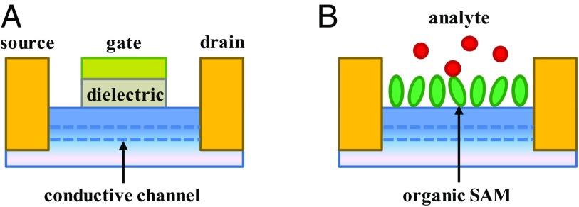
An external stimulus that produces a change in an output current is an information transfer event. Information can be transmitted via energy transfer, charge redistribution (CR), charge transfer (1, 2), spin transfer (3), field gating, etc. In a field-effect transistor (FET) (4), changing the gate voltage changes the electrostatic potential in the conductive channel between source (S) and drain (D) electrodes, thus modulating the junction current. In metal–oxide–semiconductor FETs (Fig. 1A), the semiconductor substrate is separated from the gate electrode by an insulating layer that helps to establish distinct logic states.
Fig. 1.
Schematic view of a FET (A) and a molecularly controlled semiconductor resistor (MOCSER) (B). The conduction between the source and drain through the body of the substrate (through the conductive channel) is controlled by the gate electrode potential in the first case and by the SAM polarization in the second case. The dielectric layer, which helps to maintain distinct logic stages of the FET, is provided by the alkyl chains in the MOCSER.
The electrostatic potential field that controls the conductive channel of a FET can be generated in hybrid organic–semiconductor–metal devices (Fig. 1B) (5–7). In these devices, the gate is replaced by a self-assembled monolayer (SAM) of molecules such as alkyl phosponates or dithiolated alkyls, for example. Cooperative effects in the electrostatic interactions cause delivery of a fraction of an electron charge per molecule (of the order 0.01e) from the monolayer to the substrate, which stabilizes the SAM by drastically reducing the intermolecular electrostatic repulsion (6, 8). Analyte binding to the exposed surface of the SAM causes redistribution of the electronic charge (in particular, around the SAM–substrate interface) that can change the electrostatic potential in the substrate conductive channel. Such a device is a molecular controlled semiconductor resistor (MOCSER) (5, 9–12), where the current is affected by an analyte-dependent gate voltage. Indeed, MOCSER responses can be triggered by analyte binding [including molecules of biological and biomedical relevance (13, 14)] or by radiation (15, 16).
Here, we analyze sensing mechanisms that are based on CR across the receptor element of a FET sensor. In MOCSERs, CR is accompanied by thermal fluctuations. In sensors with a solid-state receptor, CR may occur as an essentially coherent quantum process, depending on the receptor structure and temperature. In the coherent case, the sensing mechanism relies upon the analyte producing detectable charge polarization between two distant sites (see next section).
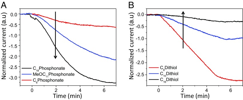
Experimentally, it was found in MOCSERs that the sensitivity of the output current to interactions with the analyte may increase with alkyl chain length (7) (Fig. 2A), that is, with decreasing coupling between the exposed surface of the receptor and its surface in contact with the substrate (Fig. 1B). This behavior would be expected in the presence of quantum coherence effects in the system response to the analyte binding . However, thermal fluctuations of the SAM produce incoherence in the electronic relaxation, due to electronic–nuclear coupling (7). Yet, the surprising distance–sensitivity relationship reported in Fig. 2 could be explained in terms of incoherent electron transfer (ET) processes through the SAM, as in the last sensing model described in the next section. Indeed, in this study, we go beyond the interpretation of the experiments of Fig. 2, to propose sensing schemes that may enable sensing by exploiting quantum mechanical properties of the detecting system (that is, without the complete loss of coherence in the sensor response to the external stimulus).
Fig. 2.
MOCSER current signal vs. time for a GaAs sensor coated with SAMs of varying thickness exposed to 10 ppm triacetone triperoxide. The signal is defined as the relative change in the current before and after exposure. The trends in the signal magnitude as a function of receptor thickness are highlighted by arrows. The SAM is adsorbed on GaAs via a (A) phosponate or (B) thiol group. The experiments are detailed in ref. 7.
Sensing controlled by coherent electronic relaxation is the main focus of this study. The general formalism adopted here produces a unified description of different quantum relaxation processes that enable chemical sensing. The models developed are, thus, widely applicable and testable. We show the richness of functionality and sensitivity that the “smart detectors” modeled here might display, and we provide design strategies to exploit their capabilities. In particular, we investigate the geometric and electronic-structure constraints on the receptor-sensing components that can produce responses to the external stimulus with intrinsically quantum mechanical characteristics. If the feasibility of the approaches described here is experimentally validated, our theoretical conclusions will enable a wide range of sensing technologies that use not only classical electrostatics but also a great variety of quantum mechanical phenomena.
Our investigation is the first step (to our knowledge) toward the rational use of classical and quantum correlations for signal transduction from a triggering event to the output current signal in FET-type sensors. The variety of quantum relaxation processes used for sensing [such as CR (7), the evolution of spin states associated with defects in solids (17), electronic energy transfer (18, 19), etc.] promises broad applications, for example in sensors that consist of nano-FET arrays (20). The mechanisms discussed here are especially relevant to processes at the nanoscale, where coherent or partially coherent quantum relaxation is more easily achieved at room temperature, compared to microscale systems.
Results and Discussion
Two-State Model for Coherent Sensing.
In this section, we discuss the basic physics behind sensing through coherent CR, using a simple two-state ( and ) model for the sensing system. The system Hamiltonian is as follows:
| [1] |
where and
| [2] |
with and . The stationary electronic state is , and the asymmetry parameter, , controls the populations of the two electronic states:
| [3] |
Perturbation by analyte binding changes the properties of state a (e.g., an electronic state localized at the analyte-binding site), and hence the coherent evolution between states a and d (e.g., a distinct electronic state whose population determines the output signal of the sensor). The perturbation can change and . For example, assuming no charge polarization before analyte binding () and after binding, the d population (midway between the initial condition and the full-polarization limit ) occurs when . Thus, the magnitude of the energy perturbation required to polarize the system decreases as drops. That is, more weakly coupled systems are more sensitive to analyte perturbation. This trend is reversed when the unperturbed system is asymmetric to begin with, namely, when .
Describing sensing with a two-state model lacks two key ingredients: (i) the two localized states may be coupled to manifolds of receptor surface states; (ii) thermal fluctuations may break the assumption of coherent quantum dynamics. Next, we consider these issues and their implications for sensing. The analysis of these issues will allow us to formulate different sensing approaches (and to provide design constraints and guidelines for their realization) that range from the coherent to the incoherent response of the sensing system to an external stimulus. Two of the sensing schemes described here may be used to interpret the experiments of Fig. 2 (see below), and discrimination between the two will require further experimental investigation. However, the broader aim of our study is to map out potentially useful molecular-sensing strategies that could be implemented and explored in experiments of the future.
Sensing via Coherent Electronic Relaxation.
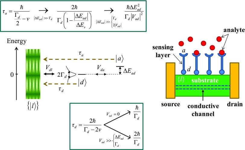
We first model sensing where the perturbing event produces a localized state of the sensing system, which then relaxes coherently to a nearly infinite manifold of one-electron substrate states (Fig. 3). For example, analyte binding produces an excess electron or hole localization (described by either or ), and the Rabi oscillation between these two states is damped by quantum relaxation to the L manifold. This transient relaxation affects the current through the junction that consists of source, conductive channel in the substrate (Fig. 1), and drain. Note that the physical model specifies neither the localization properties nor the charge donor/acceptor character of and (which is set by the initial condition).
Fig. 3.
A model for sensing based on coherent electronic relaxation. On the Left are shown the one-electron states, couplings, and characteristic times for relaxation to the substrate. A FET realization of the mechanism is shown at Right. The sensing layer (in blue) needs to be rigid enough to support coherent charge dynamics. The Insets contain limiting expressions (relevant to the discussion in the main text) for the characteristic time of quantum relaxation from the initial conditions of Eqs. 6 and 12. results from the limiting form of (Eq. 7) for . The first approximation to in the Upper Inset results from series expansion of v up to the second order in . The second approximation is consistent with CR mediation by d. The broadening of the d level by coupling to L is shown.
Two classes of sensors are considered here. In one kind, the analyte binding prepares the sensing system in the d or a state and thus initiates the quantum relaxation process. In the other case, an external stimulus other than the analyte binding (a control signal) prepares the system in the d or a state and thus gives rise to the relaxation, whereas the relaxation properties (as determined by the energy and coupling parameters in Eq. 4) depend on whether or not an analyte molecule is attached to the sensing component when the control signal is generated.
The effective electronic Hamiltonian used to model the evolution of the perturbed system is as follows:
| [4a] |
where
| [4b] |
with and, neglecting the direct a–l coupling,
| [4c] |
At time t,
| [5] |
The time evolution in Eq. 5 for the initial condition
| [6] |
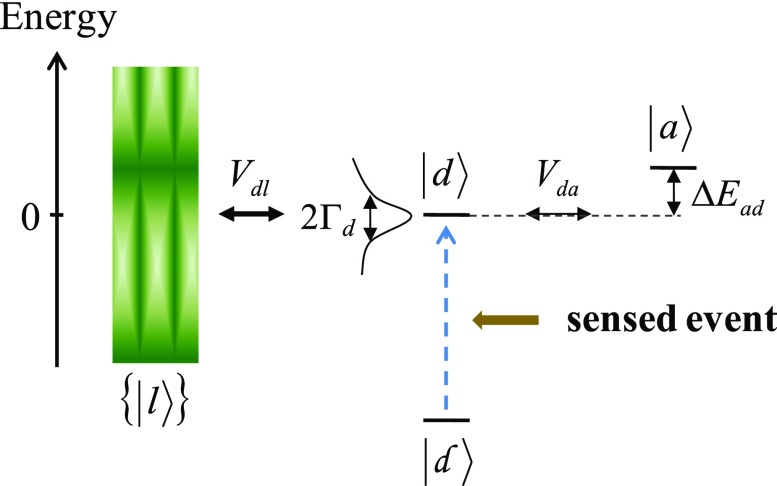
was obtained using standard approaches (2) (SI Appendix). Eq. 6 can be interpreted in different ways that allow one to apply the same model to different types of analyte interactions and/or sensor operation. These interpretations are as follows: (i) charge is captured at site d when the analyte binds to the receptor group (at t = 0), and this charge then relaxes to the L manifold. (ii) The triggering event (analyte binding or incident radiation) excites an electron charge (Fig. 4) that is stably localized on the anchoring site for to another state localized mainly on d, but with nonnegligible couplings to and . Then, the charge relaxes to the L manifold as prescribed by . (Note that this excitation–relaxation process does not require the presence of excess electron charge. The process may involve the local redistribution of an electron charge in a state of higher energy, with larger couplings to other, differently localized electronic states.) Removal of the external perturbation restores the initial localized state. (iii) is the perturbation caused by analyte binding. is an occupied frontier spin-orbital in the neutral or charged system that, after analyte binding, is coupled to the other (virtual) orbitals corresponding to . (iv) In a more elaborate sensor, charge localization on d may be induced by an external source (for example, a gate voltage applied through wiring to the substrate). The perturbation at site a produced by analyte binding influences the following charge relaxation, thus modulating the current signal. If the system is neutral, the charge localization on d and its relaxation correspond to different polarizations of the sensing system. In all of these cases, the model describes charge initially prepared on d that relaxes “irreversibly” (2) to the L manifold. This relaxation influences the electrostatic potential in the conducting channel and therefore the FET current. Note that the model described by Eqs. 4–6 also holds if and are delocalized surface states, provided that the coupling scheme in Eq. 4c is satisfied.
Fig. 4.
A model system for sensing via electronic relaxation. The charge is initially trapped in . Excitation by sensing leads to , which has nonnegligible couplings with and L (inspired by figure 9.2 of ref. 2, where is absent).
For , the time-dependent L manifold population is (SI Appendix):
| [7] |
In Eq. 7, the density of L states () was assumed independent of energy, and
| [8] |
Because , Eq. 7 describes population flow to the continuum: for (SI Appendix, Fig. S8). We now focus on the properties, and especially on the timescales, of the CR relevant to practical applications of the model. A critical issue is to reconcile the timescale of evolution (which modifies the gate voltage) with feasible current measurement times in a device. The analysis below addresses this issue and allows us to formulate design criteria for possible implementations of the sensing mechanism proposed in this section.
Charging the L manifold correlates with removing charge from the a–d system, which occurs on timescales that range from to (in Fig. 3, or , depending on the initial state of the sensor. In the timescale considerations, v is assumed positive to simplify the notation). v depends on the asymmetry , and on and (Fig. 3 and Eq. 8). When these three parameters are all of the order of a millielectronvolt, the electronic relaxation occurs on the picosecond timescale. The relaxation time can be increased by orders of magnitude by decreasing or by making v ∼ (SI Appendix). The former approach leads to a millisecond relaxation timescale for (e.g., see SI Appendix, Fig. S8; such a small value may be realized in sensor architectures with an insulating layer between the receptor and the substrate). This timescale enables ready current measurement, but coherent (or at least partially coherent) quantum-state relaxation on this millisecond timescale requires a solid-state receptor layer (in this case, defects or impurities at its surfaces may, for example, act as the a and d sites) and low enough temperatures. In general, the quantum coherence leading to Eq. 7 is lost on the millisecond timescale of Figs. 6 and 8 (see below). However, coherent state dynamics can survive for as long as microsecond or millisecond for spin excitations associated with defects in solids (21–23), which motivates use of spin relaxation as the sensing process, as an alternative to the relaxation of the spatial distribution of the electronic charge considered here. While decoherence due to the electronic–nuclear coupling is not included in our model, the properties of the electronic states and of their perturbation are kept as generic as possible. In any case, coherent electronic relaxation through the receptor is more easily obtained in nanodevices than in microelectronic devices, because of the smaller length and timescales that characterize CR in nanodevices.
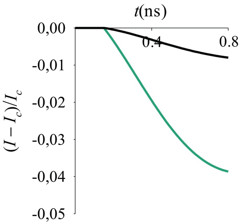
Fig. 6.
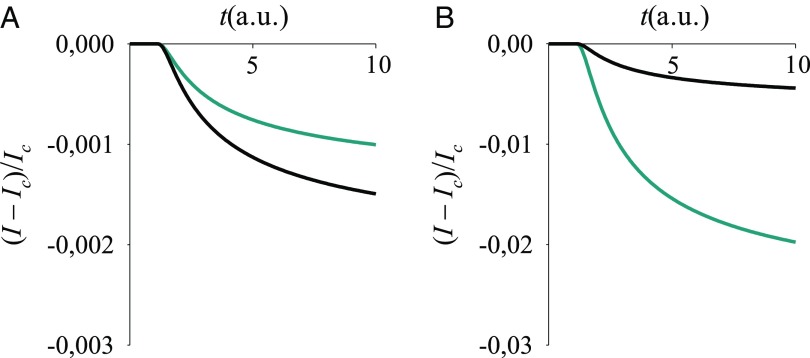
Normalized current signal vs. time, for a sensing mechanism in which a control perturbation produces the time-dependent current and the event subject to detection alters this current. Eq. 11 models the current. The model parameters are as follows: ns, , , , , (black lines) or (cyan lines), and (that is, a donor–acceptor energy gap within thermal fluctuations) before sensing, whereas this gap increases by 0.06 eV due to the sensed event.
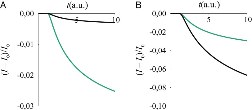
Fig. 8.
Normalized current signal vs. time for V = 1 V, with (A) or (B) , and CR induced by the sensed event starting from the initial condition in (A) Eq. 13 and (B) Eq. 6. Eqs. 17, 19, 20, and 11 were used. We set , , and in Eq. 19, hence arbitrary units (a.u.) for time (depending on the system); , , , , . The a–d coupling in the absence of analyte is () for the black (cyan) line and is doubled after binding, whereas changes in .
We now explore the physical conditions needed to produce coherent CR through a solid-state receptor on the millisecond timescale. First, we investigate FET design constraints that are required to obtain . Then, we explore the compatibility of these architectural constraints with the coherent sensing model proposed here.
We assume a semiconducting substrate density of states of ∼1 nm−3⋅eV−1 (24). For (in units of nanometers to micrometers) slabs, one obtains values in the range of to . With , the first Eq. 8 leads to in the range of to . Assuming that with and , a 25- to 40-Å-thick dielectric layer needs to be inserted between the receptor d sites and the substrate to realize the desired value. Otherwise, because in vacuum (25), one can insert a vacuum gap with z ranging from 15 to 24 Å.
These design parameters (25- to 40-Å-thick insulator or 15- to 24-Å-thick vacuum gap between receptor and substrate) are compatible with the coherent sensing mechanism based on the Hamiltonian of Eq. 4 if the transition between and is dominated by tunneling, despite the weak coupling expected at large distances. In the weak coupling regime, assuming and the two-state approximation, the system is localized on one site (for example, d) and the charge distribution tail on the other site is (Eq. 3) . Hopping through the insulator competes with d–l tunneling if the insulator thermal occupation probability is appreciable. This probability is ∼, where is Boltzmann’s constant, T is the temperature, is the effective injection energy, and g is an average electronic state degeneracy. Tunneling dominates hopping when (see ref. 26 for discussion of the hopping–tunneling transition):
| [9] |
Eq. 9 produces injection energies in the range of 0.9–2.3 eV, with g computed from the density of states, based on typical electronic effective masses and the slab sizes considered above.
The discussion above suggests that sensing through coherent electronic relaxation is accessible. The analysis provides the geometric and energetic constraints on sensor design that are needed to access a millisecond timescale with values as small as . Indeed, these constraints can be relaxed because the decay constant has the general form (Eq. 8). v depends on and , which also influence the sensitivity and time evolution of the system response to a triggering event. can be set by the receptor thickness, whereas depends on the electronegativity of the a and d sites of the receptor.
To complete our sensor model, we describe the effect of the quantum relaxation process on the FET current. The change in implies CR in the substrate (Fig. 3). We model the source-conductive channel-drain system with a bridge level of unperturbed energy that changes to the following:
| [10] |
in response to changes in . [If the initial condition of Eq. 6 is set for t = t0, t needs to be replaced by t − t0 in the expressions of all state probabilities. Then, PL(t0) = 0.] The effective interaction parameter depends on the system geometry. In fact, is proportional to the average inverse distance between the substrate surface and the conductive channel. The model describes a single sensing event that starts at (in Eq. 7, ).
Eq. 10 can be used directly in the modeling of electron transport through solid-state protein junctions (27, 28) or redox junctions (29–32). The semiconductor’s band structure should be used for quantitative descriptions of conduction through typical FET bridges. In this context, CR at the receptor–substrate interface changes the surface state-induced band bending (33).
The current through a junction with symmetric bridge–lead contacts and one bridge level (Eq. 10) is described using the Landauer–Büttiker formalism (34, 35):
| [11] |
Here, V is the bias voltage, (J = S, D) is the Fermi–Dirac distribution of electrode J, and is the molecule–electrode coupling strength that is assumed energy independent. For , increases with , thus decreasing the current for fixed bias. The sensing mechanism is valid irrespective of the conduction regime. To show this, we also consider the limit of incoherent transport via charge hopping, which is the opposite limit of coherent transport (Eq. 11). For a one-level bridge (SI Appendix, Fig. S12), the current is as follows (29, 36):
| [12] |
Here, O and R denote the oxidized and reduced bridge, respectively; is the rate constant for electron injection into the bridge from the source; is the rate of back ET to S, and and denote the ET rates at the D contact [see the t and V dependence of these rates (31) in SI Appendix].
Eqs. 11 and 12 were developed for steady-state currents, but they can also be used to describe time-dependent currents that result from the evolution of if changes sufficiently slowly for the current to adjust adiabatically to the value of . The requirement for this adiabatic response is (clearly, this condition is more easily satisfied for γ values typical of the coherent tunneling regime), that is, the timescale () for substrate–electrode ET needs to be much shorter than the characteristic time () for the electronic relaxation to the substrate and the consequent change in the gate voltage. When this condition is satisfied, the model for sensing that consists of Eqs. 7 (), 10 (), and 11 or 12 (I) produces signals as in Figs. 5 and 6 (signals on much shorter timescales are shown in SI Appendix). The influence of the triggering event on the current is similar in the Landauer–Büttiker and hopping models. The induced relative change in the current is larger for a hopping mechanism, but the absolute values of the current and its change are larger for coherent tunneling.
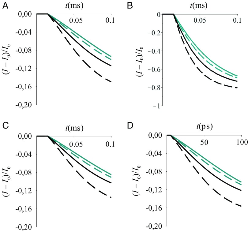
Fig. 5.
Normalized signal vs. time (t) at a bias voltage V = 1 V, from the model described by Eqs. 7, 10, and (A, C, and D) 11 or (B) 12. is the current before sensing the perturbation at ms (A–C) or ps (D). Other parameters are: , , with [as for gold (48)], (A, B, and D) or (C), , (A–C) or (D) , (black lines) or (cyan), and is (solid lines) or 0.02 eV (dashed lines). The two values chosen may simulate the effects of thermal fluctuations or of the analyte. The signal is larger for the smaller value irrespective of the value.
In Fig. 5, electronic charge transferred to the substrate surface changes the gate voltage, thus increasing and reducing the current. (Note that, depending on the localization properties of the d and {l} states, the CR produced by the electronic state relaxation from d to the L manifold may amount to a change in the substrate charge by a small fraction of an electron charge per sensed event.) The normalized current signal is , where is the constant current before sensing. I has a larger deviation from for the smaller value of (that is, the signal increases with decreasing electronic coupling between the surfaces of the receptor, as may result from using a thicker sensing element). The timescale of the signal evolution can change by orders of magnitude depending on parameters such as (Fig. 5 A and D), but the qualitative properties of the signal remain. The temperature dependence of the current does not significantly influence the normalized signal (Fig. 5 A and C). Coherence can be maintained on the timescale of Fig. 5D, unless high-frequency vibrations intervene to destroy the signal coherence. Fig. 5 shows the robustness of the sensing mechanism to a variety of physical conditions. The accessibility of such conditions in real devices needs, however, to be explored in future experiments.
In the case of Fig. 6, the electronic relaxation to the L manifold is induced by an external control mechanism or other transient phenomenon. The event of interest changes the properties of the electronic relaxation dynamics and hence of the signal produced. The electronic relaxation to the substrate is much faster than the analyte diffusion to the receptor. Therefore, each quantum relaxation process generally occurs while the sensing site is free or bound, leading to or , respectively. The magnitude of the signal increases with for the parameter choices in Fig. 6. The influence of analyte binding on the receptor properties is modeled as a change in . The signal sensitivity to this change depends on the value of with respect to the range of values sampled during sensing. In general, the thickness (which controls ), the surface chemistry (which determines ), and the rigidity of the receptor are key design parameters, as highlighted in the above analysis and further detailed in SI Appendix.
We conclude this section by considering the case where analyte binding prepares the system in an initial (quantum) state localized at the binding site a:
| [13] |
As in the case of Eq. 6, Eq. 13 may be used to describe many physical situations. The time-dependent population of the L manifold is now (SI Appendix):
| [14] |
Substituting Eq. 14 into Eq. 10 and using Eq. 11 or 12 yield signals such as those shown in Fig. 7.
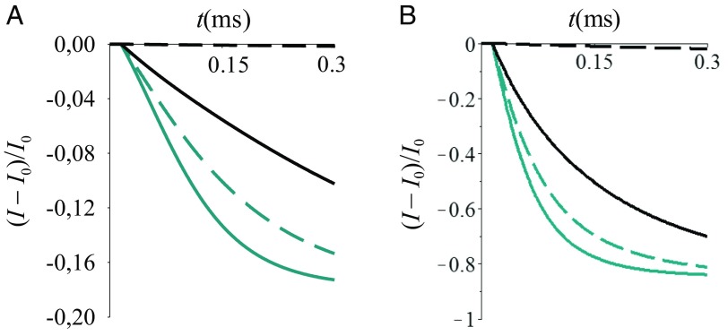
Fig. 7.
Normalized current signal vs. time, for V = 1 V, using the model that consists of Eqs. 14, 10, and (A) 11 or (B) 12. A (B) is the analog of Fig. 5A (Fig. 5B) for the initial condition in Eq. 13. The model parameters, line styles, and colors are as in Fig. 5.
In the time range shown in Fig. 7, the rate of current decrease for a given drops with increasing . This behavior, which is the opposite of that shown in Fig. 5, arises because the excess charge now is localized initially at site a, which is distal to the substrate, and the d–a Rabi oscillations required for relaxation to the L manifold of substrate states have a decreasing amplitude (as well as a decreasing average transition probability) as increases.
All of the above signals plateau to the values corresponding to or for sufficiently long observation times (e.g., see SI Appendix, Fig. S2). Hence, the signals in each figure differ by the rate of variation between the initial (before sensing) and final plateaus. This behavior was observed in the experiments of Fig. 2 at longer times. However, no quantum coherence is generally expected in these experiments, due to thermal fluctuations that are not included in the modeling of this section. The above models are relevant to sensors where the receptor and substrate support (at least partially) coherent electronic dynamics. Within the limits of applicability of such models, many facets of the pertinent quantum dynamics can be exploited in a device (e.g., the counterintuitive dependence of the signal on the a–d distance, depending on the initial charge localization, and other quantum effects described in SI Appendix).
Sensing Based on Analyte Diffusion and Coherent CR.
The model of the previous section is expanded here to include a manifold of electronic states near the exposed receptor surface that is directly coupled to , but not to and L. CR in this system (SI Appendix) may be used as in the above sensing mechanism, namely, one could conceive a (nano)detector that senses the external stimulus through the induced quantum relaxation of the sensing system state to the two manifolds of surface states in the substrate. However, the presence of two manifolds also allows us to develop a different sensing mechanism based on the charge distribution in the L and R manifolds at the end of the electronic relaxation process. In this model, the influence of the analyte on the equilibrium charge distribution between the L and R manifolds (that is, between the exposed surface of the receptor and the receptor–substrate interface) is the sensing mechanism. Analyte diffusion determines the timescale for occupation of the receptor sites (with a cumulative observable effect on the charge distribution between the L and R surface state manifolds), and thus dictates the timescale of signal detection. The electronic Hamiltonian is given by Eq. 4a with:
| [15a] |
| [15b] |
Two sensing mechanisms based on this one-electron Hamiltonian model are now examined. In one case, none of the one-electron states in Eq. 15 is occupied by the system in the absence of analyte, i.e., , , , and are virtual states. Analyte binding places the system in the a (Eq. 13) or d (Eq. 6) state. At time t,
| [16] |
The system state relaxes to L and R with a characteristic time (SI Appendix), so that the final occupation of the L manifold, which appreciably influences the gate voltage, is:
| [17] |
( is defined similarly to in Eq. 8, with a and L replacing d and R) for the initial condition in Eq. 13, or as follows:
| [18] |
for the initial condition in Eq. 6. We assume that, in the system under study, τ is negligible compared with the timescale for analyte diffusion to the receptor. This assumption is appropriate for many detectors where the analyte is sensed on second-to-minute timescales. Then, the occupation probability of L switches “instantaneously” from (or ) to the value in Eq. 17 (18) because of interaction with the analyte. This value depends on the system properties and is denoted ().
In another variant of the sensing mechanism, Eq. 17 or 18 describes the equilibrium distribution of the polarizable charge in the absence of analyte. This charge may be a valence electron of the neutral system, or an excess charge previously injected in a or d by a control external perturbation. Memory of the past evolution of the system is incorporated in the population of the L manifold before analyte binding. In fact, this population is described by Eq. 17 if the charge was initially localized at site a, or by Eq. 18 if its initial localization was at d. () is the unperturbed equilibrium value of (). The analyte changes the system properties (that is, at least one of the coupling parameters , , and ), so that ().
In both sensing mechanisms, integration of the sensing system modeled by Eq. 15 in a FET allows one to distinguish between external stimuli at the a or d sites, provided that the charge distribution in Eq. 17 or 18 is not erased by thermal fluctuations and/or “communication” between the L and R manifolds on the timescale of the measurement. In fact, when analyte binding causes displacement of charge initially localized on site a, decreasing (i.e., thickening the receptor layer; Fig. 3) decreases charge storage in L (Eq. 17). In contrast, if the analyte causes charge displacement from d, thickening the receptor increases the L manifold population (Eq. 18). Thus, depending on the electronic properties of the system and on the localization of the external stimulus, changes of the current from the unperturbed stationary value may increase or decrease with increasing receptor thickness, as described by the dependence of the substrate surface state (L) population on the d–a coupling in Eqs. 17 and 18, and shown in Figs. 8 and 9. Selective sensing in enabled by responses such as those illustrated in Figs. 8 A and B or 9 A and B (namely, by application of the present sensing model) if different analyte species produce different initial charge redistributions in the receptor, according to Eqs. 17 and 18. The FET output signals in these figures are obtained by combining the above model for CR induced by analyte binding with a model for the analyte diffusion to the exposed surface of the receptor.
Fig. 9.
Normalized current signal vs. time, using Eq. 13 and for . is the current in the absence of analyte. is obtained by using and Eq. 20 with p = 0. Eqs. 17, 19, 20, and 11 are used. After analyte binding, and change in (A) and (B) . The other parameters and the color code are the same as in Fig. 8.
We model diffusion of the analyte as a one-dimensional process that obeys Fick’s second law with boundary conditions of constant analyte concentration at a distance y above the top of the receptor, where the a sites are located. If diffusion begins at a , the joint probability that an analyte molecule reaches the sensing surface and interacts with any receptor site a at time t is:
| [19] |
D is the diffusion coefficient and is the interaction (or binding) probability. In contrast to the model of the previous section, it is not necessary to have very small values of and to obtain current signals on a long timescale, since the timescale of the change in the current is determined by analyte diffusion. Hence, the model may also be applied to the MOCSERs if the timescale of molecular motion is longer than that of electronic relaxation, if the charge distribution in Eq. 17 or 18 is sufficiently stable with respect to molecular motion, and if the influence of the nuclear motion on the charge distribution does not erase or exceed the CR produced by the sensed event.
To describe conduction through the FET junction, the energy of the bridge level is modeled as follows:
| [20] |
when Eq. 17 is used. is replaced by in Eq. 20 when Eq. 18 is used. or is zero for the sensing mechanism where the triggering event creates the charge distribution in Eq. 17 or 18.
The model for sensing on the timescale of analyte diffusion described in this section consists of Eqs. 19 (analyte diffusion), 17 or 18 (CR in the substrate, near the receptor, due to the analyte), and 11 (current). The cases (first sensing mechanism) and (second sensing mechanism) are considered in Figs. 8 and 9. As expected from Eqs. 17 and 18, the decrease in the current is more (less) pronounced with increasing if the external perturbation occurs at the a (d) site (compare Fig. 9 A and B). For , the dependence of the signal on can be inverted, depending on the changes in and caused by the analyte.
We expect that the conditions for the applicability of the present model to MOCSERs (see above) are likely very difficult to achieve, because thermal fluctuations and the long-range coupling between the L and R manifolds in most such molecular sensors can erase the charge distribution described by Eqs. 17 and 18. However, if the conditions of validity for the present model are satisfied (e.g., in systems were nuclear fluctuations are not effective in erasing the electronic charge distribution of Eqs. 17 and 18; note, however, that the feasibility of this condition needs to be established experimentally), our theoretical analysis yields the chemical–physical underpinnings of signals such as those in Fig. 2. In this case, Fig. 2 can be directly compared with Fig. 8 or Fig. 9.
Decoherence between the L and R populations, which may arise when the direct L–R couplings cannot be disregarded as in Eq. 15b, would erase the information on the localization of the external stimulus at the a or d site, but would allow for a different sensing mechanism, as shown in the next section.
Sensing Based on Analyte Diffusion and Incoherent CR.
The couplings between L and R states were neglected above because they were assumed to be sufficiently small that they have a negligible effect on the timescale of coherent CR. (The a–L and d–R couplings are not included in the model, because the occupation probabilities of the a and d sites are neglected on the τincoherent timescale.) In contrast, these couplings may be nonnegligible and produce incoherent CR on a timescale . We describe CR between L and R in terms of equilibration of ET between the two manifolds of states. This model may describe the experimental data in Fig. 2. In fact, in the underlying experiments, the receptor is a (flexible) molecular layer and the current signal is generated by analyte diffusion on a minute timescale.
Another assumption of the sensing model in this section is that analyte diffusion to the receptor occurs on a timescale that is longer than . The binding of analyte to the a sites perturbs the energy differences among the L and R states (hence, the L–R free-energy difference), thus leading to CR (repolarization) and to a consequent change in the electrostatic potential field in the conductive channel.
Incoherent CR is described by the classical master equations:
| [21a] |
| [21b] |
In Eq. 21, () is the rate constant for ET from to (from to ). In this simple model, we assume that the ET rates are described by Marcus nonadiabatic ET theory. For , the quantum information encoded in the L and R populations for is lost. Assuming an average energy difference between L and R states, this simple model leads to the Boltzmann result (see SI Appendix for the definition of ):
| [22] |
Analyte binding changes to , and thus alters . Using an electrostatic model for and making a multipole expansion of the charge distribution on an analyte particle (e.g., TATP in ref. 7), one obtains the following:
| [23] |
where Λ is an effective distance between the regions where the L and R populations are distributed. Λ is approximated by the average a–d distance if L and R are manifolds of surface electronic states. After modeling Λ, one may obtain time-dependent currents similar to those in Fig. 2 using Eq. 22 in combination with Eq. 19 for the analyte diffusion, Eq. 20 for an effective bridge energy level in the junction, and Eq. 11 or 12 (or a band model) for the conduction. The model predicts that the output current signal increases or decreases with increasing Λ (as in the experiments of Fig. 2), depending on the expansion coefficients in Eq. 23 and, especially, on the sign of . More detailed applications of this incoherent model require estimates of and are beyond the scope of the present study. The models developed above are summarized in Table 1.
Table 1.
Summary of sensing models developed here
| Model | Coherent two-state dynamics | Coherent multistate dynamics (hence CR) after analyte binding | Analyte diffusion and coherent CR | Analyte diffusion and incoherent CR |
| Assumptions | Reversible coherent dynamics in the two-state approximation. | A localized electronic state produced by the analyte binding irreversibly relaxes to a dense manifold of states at the receptor–substrate interface. | A localized state irreversibly relaxes to two manifolds of states at the exposed surface of the receptor and at the receptor–substrate interface. | Thermal fluctuations of the atoms in the receptor lead to incoherent CR. |
| Special properties | Sensing exclusively based on quantum relaxation processes. | Quantum effects are incorporated in the CR between the state manifolds induced by each binding event. | Incoherent CR during the analyte diffusion erases the quantum effects. The binding of the analyte perturbs the energy differences between the two manifolds of states, thus leading to CR. | |
| Results | A weaker coupling implies a higher sensitivity to the perturbation when the unperturbed states have similar energies. | The event of interest causes the electronic state relaxation (hence a signal in the actuator) or changes the properties of electronic relaxation produced by an external control mechanism or transient phenomenon. The timescale of the electronic relaxation characterizes the observed nanosensor output signal. | The equilibrium charge distribution between exposed surface of the receptor and receptor–substrate interface determines the signal, whereas the diffusion of the analyte dictates the timescale of the signal. Special conditions are required to apply this model to MOCSERs. | The model predicts that the actuator’s signal may increase or decrease with increasing length of the receptor molecules in a MOCSER. |
| Limits of applicability | Coupling to bulk states and thermal fluctuations that can break the assumption of coherent quantum dynamics are not included. | Incoherence that arises from thermal fluctuations is not included (hence needs to be negligible for the applicability of the model). | The coupling between the two manifolds of states that may induce decoherence is not included and would erase the information on the initial localization of the external perturbation. |
Conclusions
We have provided a theoretical framework and designed guidelines for molecular-sensing devices based fundamentally on quantum dynamical effects. The theory links different sensing mechanisms and establishes the limits for their applicability, depending on FET device architectures and material properties. The coherent charge relaxation models require the use of solid-state materials for their implementation. One of the possible applications is, for example, to insulated and suspended gate FET devices (37, 38) that may use a selective layer made of conducting polymer (37). Application of the proposed sensing mechanisms to the devices in refs. 37 and 38 would require assessing both (i) the degree of coherence attainable and necessary for operation, and (ii) the measurement timescales allowed by different types of receptors. In other classes of sensors, the perturbing event directly changes the conductivity of a film between source and drain (39–45), and thus only one manifold of surface states should be used to model these systems.
Polaron models (2, 46) may be used to describe the receptor–substrate system and the conduction through the FET junction in future extensions of this study. The quantum master equation (2) or the reduced hierarchy equations of motion approaches (47) could be used to develop a general treatment of the incoherent evolution of the system after analyte binding. Our study (i) offers an in-depth analysis of sensing based upon coherent quantum relaxation processes, including device design constraints; (ii) affords a clear framework for future research; (iii) fosters explicit links between chemical sensing and quantum information theory, thus paving the way to use coherent control techniques (21) for molecular sensing. However, the feasibility of the proposed mechanisms for chemical sensing in practical detectors needs and deserves to be further studied theoretically and to be explored experimentally, in light of the encouraging comparisons with the experimental data of Fig. 2.
Supplementary Material
Acknowledgments
We thank Prof. Peng Zhang of Duke University and Prof. Spiros Skourtis of the University of Cyprus for helpful discussions. We also thank Dr. Tali Aqua and Dr. Eyal Capua from the Weizmann Institute of Science for experimental studies associated with Fig. 2. We also thank the US Department of Energy for support of this research (Grant SC0010662).
Footnotes
The authors declare no conflict of interest.
This article is a PNAS Direct Submission.
This article contains supporting information online at www.pnas.org/lookup/suppl/doi:10.1073/pnas.1502000112/-/DCSupplemental.
References
- 1.Marcus RA, Sutin N. Electron transfers in chemistry and biology. Biochim Biophys Acta. 1985;811(3):265–322. [Google Scholar]
- 2.Nitzan A. Chemical Dynamics in Condensed Phases. Oxford Univ Press; Oxford: 2007. [Google Scholar]
- 3.Wolf SA, et al. Spintronics: A spin-based electronics vision for the future. Science. 2001;294(5546):1488–1495. doi: 10.1126/science.1065389. [DOI] [PubMed] [Google Scholar]
- 4.Lilienfeld JE. 1930. Method and apparatus for controlling electric currents. US Patent 1,745,175.
- 5.Gartsman K, et al. Molecular control of a GaAs transistor. Chem Phys Lett. 1998;283(5-6):301–306. [Google Scholar]
- 6.Cahen D, Naaman R, Vager Z. The cooperative molecular field effect. Adv Funct Mater. 2005;15(10):1571–1578. [Google Scholar]
- 7.Capua E, Cao R, Sukenik CN, Naaman R. Detection of triacetone triperoxide (TATP) with an array of sensors based on non-specific interactions. Sens Actuators B Chem. 2009;140(1):122–127. [Google Scholar]
- 8.Taylor DM, Bayes GF. Calculating the surface potential of unionized monolayers. Phys Rev E Stat Phys Plasmas Fluids Relat Interdiscip Topics. 1994;49(2):1439–1449. doi: 10.1103/physreve.49.1439. [DOI] [PubMed] [Google Scholar]
- 9.Vilan A, et al. Real-time electronic monitoring of adsorption kinetics: Evidence for two-site adsorption mechanism of dicarboxylic acids on GaAs(100) J Phys Chem B. 1998;102(18):3307–3309. [Google Scholar]
- 10.Wu DG, et al. Novel NO biosensor based on the surface derivatization of GaAs by “hinged” iron porphyrins. Angew Chem Int Ed Engl. 2000;39(24):4496–4500. [PubMed] [Google Scholar]
- 11.Vilar MR, et al. Development of nitric oxide sensor for asthma attack prevention. Mat Sci Eng C-Biomim. 2006;26(2-3):253–259. [Google Scholar]
- 12.Capua E, Natan A, Kronik L, Naaman R. The molecularly controlled semiconductor resistor: How does it work? ACS Appl Mater Interfaces. 2009;1(11):2679–2683. doi: 10.1021/am9005622. [DOI] [PubMed] [Google Scholar]
- 13.Bavli D, et al. Detection and quantification through a lipid membrane using the molecularly controlled semiconductor resistor. Langmuir. 2012;28(1):1020–1028. doi: 10.1021/la203502b. [DOI] [PubMed] [Google Scholar]
- 14.Tatikonda AK, Tkachev M, Naaman R. A highly sensitive hybrid organic-inorganic sensor for continuous monitoring of hemoglobin. Biosens Bioelectron. 2013;45:201–205. doi: 10.1016/j.bios.2013.01.040. [DOI] [PubMed] [Google Scholar]
- 15.Aqua T, Naaman R, Aharoni A, Banin U, Paltiel Y. Hybrid nanocrystals-organic-semiconductor light sensor. Appl Phys Lett. 2008;92(22):223112. [Google Scholar]
- 16.Naaman R. Molecular controlled nano-devices. Phys Chem Chem Phys. 2011;13(29):13153–13161. doi: 10.1039/c1cp21106d. [DOI] [PubMed] [Google Scholar]
- 17.Kolkowitz S, et al. Coherent sensing of a mechanical resonator with a single-spin qubit. Science. 2012;335(6076):1603–1606. doi: 10.1126/science.1216821. [DOI] [PubMed] [Google Scholar]
- 18.Sarovar M, Ishizaki A, Fleming GR, Whaley KB. Quantum entanglement in photosynthetic light-harvesting complexes. Nat Phys. 2010;6(6):462–467. [Google Scholar]
- 19.Ishizaki A, Fleming GR. Quantum coherence in photosynthetic light harvesting. Annu Rev Condens Matter Phys. 2012;3:333–361. doi: 10.1098/rsta.2011.0207. [DOI] [PubMed] [Google Scholar]
- 20.Lichtenstein A, et al. Supersensitive fingerprinting of explosives by chemically modified nanosensors arrays. Nat Commun. 2014;5:4195. doi: 10.1038/ncomms5195. [DOI] [PubMed] [Google Scholar]
- 21.Rego LGC, Santos LF, Batista VS. Coherent control of quantum dynamics with sequences of unitary phase-kick pulses. Annu Rev Phys Chem. 2009;60:293–320. doi: 10.1146/annurev.physchem.040808.090409. [DOI] [PubMed] [Google Scholar]
- 22.Jelezko F, Gaebel T, Popa I, Gruber A, Wrachtrup J. Observation of coherent oscillations in a single electron spin. Phys Rev Lett. 2004;92(7):076401. doi: 10.1103/PhysRevLett.92.076401. [DOI] [PubMed] [Google Scholar]
- 23.Christle DJ, et al. Isolated electron spins in silicon carbide with millisecond coherence times. Nat Mater. 2015;14(2):160–163. doi: 10.1038/nmat4144. [DOI] [PubMed] [Google Scholar]
- 24.Mishra UK, Singh J. Semiconductor Device Physics and Design. Springer; Dordrecht, The Netherlands: 2008. [Google Scholar]
- 25.Jones ML, Kurnikov IV, Beratan DN. The nature of tunneling pathway and average packing density models for protein-mediated electron transfer. J Phys Chem A. 2002;106(10):2002–2006. [Google Scholar]
- 26.Berlin YA, Burin AL, Ratner MA. Elementary steps for charge transport in DNA: Thermal activation vs. tunneling. Chem Phys. 2002;275(1-3):61–74. [Google Scholar]
- 27.Ron I, et al. Proteins as electronic materials: Electron transport through solid-state protein monolayer junctions. J Am Chem Soc. 2010;132(12):4131–4140. doi: 10.1021/ja907328r. [DOI] [PubMed] [Google Scholar]
- 28.Amdursky N, Ferber D, Pecht I, Sheves M, Cahen D. Redox activity distinguishes solid-state electron transport from solution-based electron transfer in a natural and artificial protein: Cytochrome C and hemin-doped human serum albumin. Phys Chem Chem Phys. 2013;15(40):17142–17149. doi: 10.1039/c3cp52885e. [DOI] [PubMed] [Google Scholar]
- 29.Kuznetsov AM, Ulstrup J. Mechanisms of in situ scanning tunnelling microscopy of organized redox molecular assemblies. J Phys Chem A. 2000;104(49):11531–11540. [Google Scholar]
- 30.Kuznetsov AM. Negative differential resistance and switching behavior of redox-mediated tunnel contact. J Chem Phys. 2007;127(8):084710. doi: 10.1063/1.2770725. [DOI] [PubMed] [Google Scholar]
- 31.Migliore A, Nitzan A. Nonlinear charge transport in redox molecular junctions: A Marcus perspective. ACS Nano. 2011;5(8):6669–6685. doi: 10.1021/nn202206e. [DOI] [PubMed] [Google Scholar]
- 32.Migliore A, Nitzan A. Irreversibility and hysteresis in redox molecular conduction junctions. J Am Chem Soc. 2013;135(25):9420–9432. doi: 10.1021/ja401336u. [DOI] [PubMed] [Google Scholar]
- 33.Zhang Z, Yates JT., Jr Band bending in semiconductors: Chemical and physical consequences at surfaces and interfaces. Chem Rev. 2012;112(10):5520–5551. doi: 10.1021/cr3000626. [DOI] [PubMed] [Google Scholar]
- 34.Schmickler W. Investigation of electrochemical electron transfer reactions with a scanning tunneling microscope: A theoretical study. Surf Sci. 1993;295(1-2):43–56. [Google Scholar]
- 35.Di Ventra M. Electrical Transport in Nanoscale Systems. Cambridge Univ Press; New York: 2008. [Google Scholar]
- 36.Sumi H. Phonon-progressional V-I characteristics of STM processes mediated by redox molecular adsorbates. Chem Phys. 1997;222(2-3):269–280. [Google Scholar]
- 37.Janata J, Josowicz M. Chemical modulation of work function as a transduction mechanism for chemical sensors. Acc Chem Res. 1998;31(5):241–248. [Google Scholar]
- 38.Kanechika M, et al. A vertical insulated gate AlGaN/GaN heterojunction field-effect transistor. Jpn J Appl Phys. 2007;46(21):L503–L505. [Google Scholar]
- 39.Paul EW, Ricco AJ, Wrighton MS. Resistance of polyaniline films as a function of electrochemical potential and the fabrication of polyaniline-based microelectronic devices. J Phys Chem. 1985;89(8):1441–1447. [Google Scholar]
- 40.McQuade DT, Pullen AE, Swager TM. Conjugated polymer-based chemical sensors. Chem Rev. 2000;100(7):2537–2574. doi: 10.1021/cr9801014. [DOI] [PubMed] [Google Scholar]
- 41.Zhao D, Swager TM. Sensory responses in solution vs solid state: A fluorescence quenching study of poly(iptycenebutadiynylene)s. Macromolecules. 2005;38(22):9377–9384. [Google Scholar]
- 42.Thomas SW, 3rd, Joly GD, Swager TM. Chemical sensors based on amplifying fluorescent conjugated polymers. Chem Rev. 2007;107(4):1339–1386. doi: 10.1021/cr0501339. [DOI] [PubMed] [Google Scholar]
- 43.García-Berríos E, et al. Response versus chain length of alkanethiol-capped Au nanoparticle chemiresistive chemical vapor sensors. J Phys Chem C. 2010;114(50):21914–21920. [Google Scholar]
- 44.García-Berríos E, et al. Response and discrimination performance of arrays of organothiol-capped Au nanoparticle chemiresistive vapor sensors. J Phys Chem C. 2011;115(14):6208–6217. [Google Scholar]
- 45.Rochat S, Swager TM. Conjugated amplifying polymers for optical sensing applications. ACS Appl Mater Interfaces. 2013;5(11):4488–4502. doi: 10.1021/am400939w. [DOI] [PubMed] [Google Scholar]
- 46.Galperin M, Ratner MA, Nitzan A. Hysteresis, switching, and negative differential resistance in molecular junctions: A polaron model. Nano Lett. 2005;5(1):125–130. doi: 10.1021/nl048216c. [DOI] [PubMed] [Google Scholar]
- 47.Tanaka M, Tanimura Y. Multistate electron transfer dynamics in the condensed phase: Exact calculations from the reduced hierarchy equations of motion approach. J Chem Phys. 2010;132(21):214502. doi: 10.1063/1.3428674. [DOI] [PubMed] [Google Scholar]
- 48.Xu Y, Schoonen MAA. The absolute energy positions of conduction and valence bands of selected semiconducting minerals. Am Mineral. 2000;85(3-4):543–556. [Google Scholar]
Associated Data
This section collects any data citations, data availability statements, or supplementary materials included in this article.


