Abstract
Organolead halide perovskites have attracted substantial attention because of their excellent physical properties, which enable them to serve as the active material in emerging hybrid solid-state solar cells. Here we investigate the phototransistors based on hybrid perovskite films and provide direct evidence for their superior carrier transport property with ambipolar characteristics. The field-effect mobilities for triiodide perovskites at room temperature are measured as 0.18 (0.17) cm2 V−1 s−1 for holes (electrons), which increase to 1.24 (1.01) cm2 V−1 s−1 for mixed-halide perovskites. The photoresponsivity of our hybrid perovskite devices reaches 320 A W−1, which is among the largest values reported for phototransistors. Importantly, the phototransistors exhibit an ultrafast photoresponse speed of less than 10 μs. The solution-based process and excellent device performance strongly underscore hybrid perovskites as promising material candidates for photoelectronic applications.
 Organolead halide perovskites exhibit good optoelectronic properties. Here, the authors fabricated and characterized ambipolar phototransistors based on solution-processed organolead triiodide and mixed-halide perovskites exhibiting high electron and hole mobilities and high photoresponsivities.
Methylammonium lead halide (CH3NH3PbX3, X=halogen) perovskites have been intensively pursued as light-harvesting materials in high-performance hybrid solid-state photovoltaic devices1,2,3,4,5,6,7,8,9,10,11,12,13. This class of materials was first discovered by Weber nearly 36 years ago14, and Mitzi and co-workers further revealed that halide perovskites combine the favourable carrier transport of inorganic semiconductors with the facile processing of organic materials15. In their pioneering work on field-effect transistors using hybrid perovskite (C6H5C2H4NH3)2SnI4 as channels, a high on/off ratio of 104 and a hole mobility of 0.6 cm2 V−1 s−1 were reported16. The recent successes of halide perovskites in photovoltaic technologies can be primarily ascribed to their suitable, direct bandgap with large absorption coefficients and low-cost solution-based processing, as well as their excellent transport properties17,18,19,20. Long electron–hole diffusion lengths and carrier lifetimes have also been observed in perovskite films, indicating low recombination rates of charge carriers21,22. The properties of these emerging materials also led to photoelectronic applications, such as electrically pumped lasers, light-emitting diode/transistors and photodetectors23,24,25,26,27,28,29,30,31. Supplementary Table 1 summarizes the recent progresses on developing perovskite-based photodetectors. These hybrid perovskites can also be envisioned as good candidates for phototransistor, in which the gate bias, in addition to the incident light, is used as an additional parameter to modulate the channel transport32,33. Various types of semiconductors have been investigated as channel materials in phototransistors, such as Si, III–V semiconductors, ZnO, carbon nanotubes, quantum dots, organics and two-dimensional materials34,35,36,37,38,39,40,41,42,43,44,45,46,47,48,49. To date, there have been some pioneering lines of work on utilizing CH3NH3PbX3 as the active component in phototransistor-type devices27,29,30. However, the performance of these devices, particularly channel mobility and gate tuning, needs improvements.
In this work, we report on the fabrication and characterization of phototransistors on the basis of solution-processed organolead triiodide (CH3NH3PbI3) and mixed-halide (CH3NH3PbI3−xClx) perovskite films. The effects of gate voltage and light illumination on the transport of the perovskite channels were investigated. We found that these phototransistors exhibit clear ambipolar carrier transport characteristics, that is, they work in both accumulation (p-type) and inversion (n-type) modes. Highly balanced photo-induced carrier mobilities of 0.18 cm2 V−1 s−1 (holes) and 0.17 cm2 V−1 s−1 (electrons) were observed for CH3NH3PbI3, which increase to 1.24 cm2 V−1 s−1 (holes) and 1.01 cm2 V−1 s−1 (electrons) for the doped variant CH3NH3PbI3−xClx. As an important figure-of-merit for phototransistors, the photoresponsivity (R) of our perovskite phototransistor reaches 320 A W−1. Furthermore, we observed that the phototransistors exhibit an ultrafast photoresponse time of less than 10 μs. The results indicate that solution-processed hybrid perovskites are very promising materials for constructing high-performance phototransistors, and they warrant exploration for use in other photoelectronic applications.
Results
Hybrid perovskite phototransistor
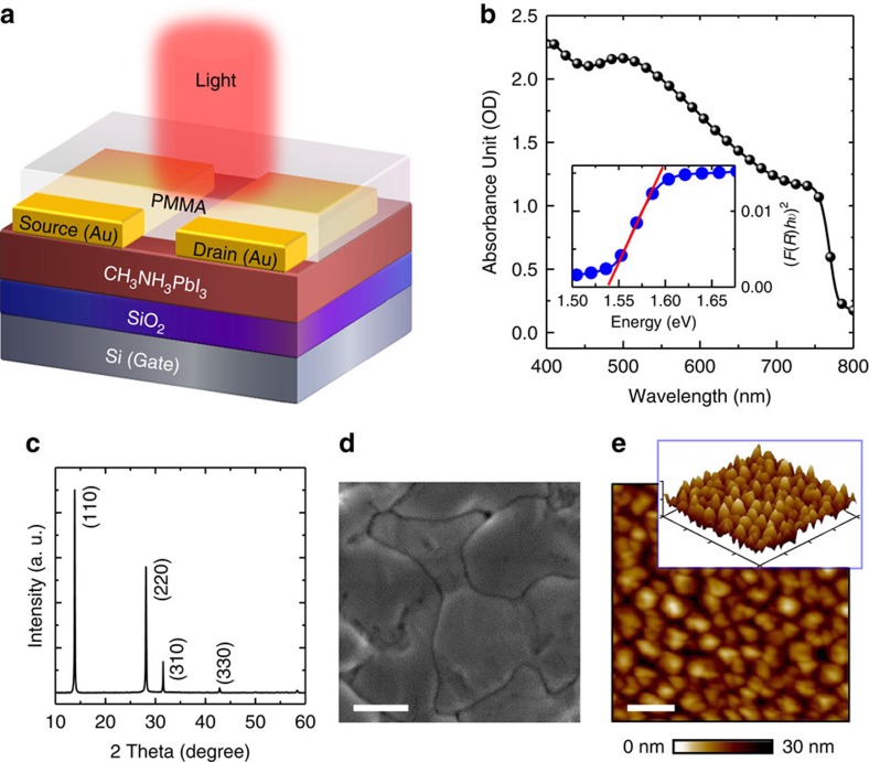
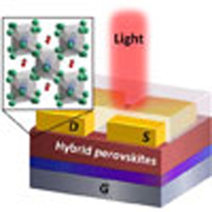
A schematic device structure of a bottom-gate, top-contact hybrid perovskite CH3NH3PbI3-based phototransistor is illustrated in Fig. 1a. A heavily n-doped Si wafer with a 300-nm SiO2 surface layer (capacitance (Ci) of 15 nF cm−2) was employed as the substrate. The perovskite films were grown using the two-step vapour-assisted solution process11, and the experimental details are given in the Methods section. In our devices, we coated poly(methyl methacrylate) (PMMA) as the protective layer on top of the perovskite channel to prevent the diffusion of moisture and/or atmospheric oxygen21. In optimizing phototransistor devices, the semiconducting channel thickness is a key parameter. On the one hand, if the semiconducting channel is too thin, it will not absorb sufficient light10. In addition, pinholes in the thin perovskite films will cause inhomogeneous conduction in the channel. On the other hand, if the film is too thick, light from the top may not be able to penetrate the whole film, and the bottom gate will not effectively modulate the channel. In our work, the thickness of the CH3NH3PbI3 film prepared in the phototransistors is optimized at 100 nm, as characterized using atomic force microscopy (AFM)50. The detailed AFM measurement results are shown in Supplementary Fig. 1.
Figure 1. Hybrid perovskite phototransistors.
(a) Schematic of the phototransistor with a channel of hybrid perovskite CH3NH3PbI3. (b) Ultraviolet–visible absorption of the 100-nm CH3NH3PbI3 film. The inset shows a direct bandgap of ∼1.53 eV. (c) X-ray diffraction spectrum of the CH3NH3PbI3 film. (d) Top-view SEM image of the perovskite film. Scale bar, 0.5 μm. (e) Tapping-mode AFM height image of the perovskite film. Scale bar, 1.0 μm. Inset: the corresponding three-dimensional topographic image.
Figure 1b shows the light absorption data of the CH3NH3PbI3 film. For this measurement, the thin films were prepared on a glass substrate using the same processing parameters as those used in fabricating the phototransistors. The strong and broad absorption in the ultraviolet and visible-light range, particularly from 400 to 760 nm, reveals that the perovskite layer is a good light absorber. Furthermore, the absorption edge for the perovskite film is very sharp, suggesting a direct bandgap nature7,18. Overall, the direct bandgap of 1.53 eV and the favourable light absorption properties make perovskite CH3NH3PbI3 films very promising materials for constructing high-performance phototransistors.
Characterizations of the perovskite thin films
To investigate the crystallinity and microstructure of the perovskite thin films, X-ray diffraction (XRD) measurements were carried out. Figure 1c shows the X-ray diffraction pattern of the as-prepared CH3NH3PbI3 film on a SiO2/Si substrate. Strong peaks at 14.08°, 28.41°, 31.85° and 43.19° can be assigned to (110), (220), (310) and (330) diffractions of CH3NH3PbI3, respectively, indicating that the halide perovskite films possess the expected orthorhombic crystal structure with high crystallinity17. Notably, the absence of a diffraction peak at 12.65° suggests that the level of the PbI2 impurity phase is negligible11. The surfaces of the perovskite CH3NH3PbI3 films were further evaluated via scanning electron microscopy (SEM) and AFM measurements. Figure 1d shows the surface morphology of the as-grown perovskite thin film grown on the SiO2/Si substrate. The perovskite film appears smooth without pinholes, and the uniform grains have sizes up to hundreds of nanometres. These structural characters are promising for achieving high performance in phototransistors. As shown in Fig. 1e, the film surface was also characterized using AFM, and the root-mean-square roughness is ∼10.5 nm in a typical scanning area of 5.0 μm × 5.0 μm. The three-dimensional AFM image in the inset of Fig. 1e further demonstrates the smooth surface of the perovskite film.
Phototransistor characterization
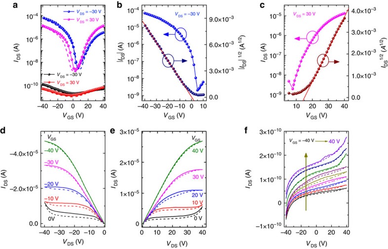
Figure 2a shows a representative set of the transfer characteristics, which are the drain current versus gate voltage (IDS−VGS) data, of a bottom-gate top-contact CH3NH3PbI3 phototransistor. The devices were measured both in the dark and under white-light illumination (power density: 10 mW cm−2) at the drain voltages (VDS) of −30 and 30 V. An ambipolar high performance can be clearly observed in the transfer characteristics under light illumination, and the V shape of the transfer curves is similar to those of previous reports on ambipolar transistors51,52,53,54,55,56. The current of the illuminated channel can reach 0.1 mA. In contrast, for the transfer characteristics measured under the dark condition, IDS, remains below 0.5 nA.
Figure 2. Ambipolar characteristics of the hybrid perovskite phototransistors.
(a) Transfer characteristics of a perovskite-based phototransistor in the dark (black and red symbols) and under light illumination (blue and magenta symbols). (b,c) Representation of the transfer characteristics of p-channel and n-channel behaviours, respectively, under light illumination. (d,e) Respective output properties of the device under light condition. (f) Output curves of the phototransistor in the dark condition. Solid and dashed curves were measured during forward and backward sweepings, respectively.
Figure 2b,c shows the plots of IDS1/2 and IDS as functions of VGS for the perovskite phototransistor measured under light illumination. The plots appear linear for a large range of VGS for both p- and n-type transports. The field-effect mobility (μ) and threshold voltage (VTH) can be extracted using the saturated IDS versus VGS relationship52,53:
 |
where W, L and Ci are the channel width, the channel length and the gate capacitance per unit area, respectively. Accordingly, the photo-induced hole and electron mobilities are derived as 0.18 and 0.17 cm2 V−1 s−1, respectively, in the saturation region. Thus, it is clear that under light illumination the perovskite-based phototransistor exhibits ambipolar behaviour with balanced hole and electron mobilities.
Under light illumination, the output characteristics (that is, IDS versus VDS data at different VGS) obtained for the device operating in the hole-enhancement and electron-enhancement modes are displayed in Fig. 2d,e, respectively. At low VGS, the device exhibits ambipolar transport with diode-like current–voltage (I–V) characteristics; however, at high VGS, unipolar transport with standard linear-to-saturation I–V transistor characteristics was observed. Figure 2f shows the output characteristics of the phototransistor measured in the dark. It can be clearly seen that there is no obvious field effect, and IDS remains at the level of 10−10 A, which is consistent with the transfer characteristics.
For measurements performed in the dark, as shown in Fig. 2a, IDS remains less than 0.5 nA when VGS increases from −40 to +40 V, and the obtained on/off ratio is less than 10. In contrast, regarding device performance under light illumination, the on current is significantly enhanced to 10−4 A, while the off current also increases to 2.0 × 10⁻⁹ A. Furthermore, the on/off ratios under illumination are boosted to 3.32 × 10⁴ for p-type and 8.76 × 10³ for n-type transports. The significant gate-tuning effect on illumination with respect to the dark measurements implies that the photo-excited carriers dominate the channel transport; thus, the device has potential for use in other photoelectronic applications such as photosensors.
Furthermore, it should be noted that both the transfer curves and the output curves exhibit weak but notable hysteresis effects (Fig. 2), which were also reported for solar cells, memristors and light-emitting field-effect transistors on the basis of hybrid perovskites31,57,58,59. One origin of the hysteresis effects was speculated to be the screening effects arisen from the field-induced drift of methylammonium cations59. In addition, charge traps and surface dipoles at the untreated semiconductor–dielectric interface may also attribute to the hysteresis effect53. In Fig. 2, the hysteresis effect in the phototransistor operation is not substantial, which is presumably a result of the high quality of the perovskite films.
To examine the effect of the device structure, we also fabricated a bottom-gate bottom-contact perovskite phototransistor (schematic shown in Supplementary Fig. 2). Supplementary Fig. 3 shows the ambipolar transfer characteristics of the devices under light illumination, which is similar to that of the bottom-gate top-contact devices. In this particular device, both the electron and hole mobilities were measured as 0.17 cm2 V−1 s−1, suggesting a very balanced ambipolar transport under light illumination. These results reveal that the ambipolar performance of phototransistors is an intrinsic property of CH3NH3PbI3 and is independent of the device architecture.
Photoresponsivity (R) is the key parameter for evaluating the performance of phototransistors, and its value can be obtained using transfer characteristics. R is given by the following equation:
 |
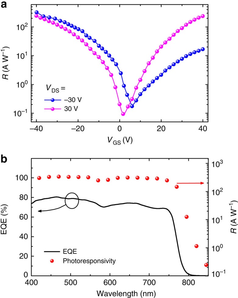
where Ilight and Idark stand for the drain currents under light illumination and in the dark, respectively, and Elight is the power of incident illumination. R as a function of VGS is shown in Fig. 3a. The maximum R value of 320 A W−1 in the On state (VGS=−40 V) was obtained at a power density of 10 mW cm−2. We also examined the phototransistors with various perovskite film thicknesses (shown in Supplementary Fig. 4), and we found that the performance of devices with the active layer thickness of ∼100 nm is optimal. Note that this parameter achieved in perovskite phototransistors is substantially higher than those of most other reported functional materials38,40,42,43,44,45,47,48. For example, phototransistors based on organic semiconductors and hybrid materials were reported with R values typically below 1.0 A W−1 (ref. 45). This superb performance of hybrid perovskites in phototransistors can be attributed to their excellent light absorption properties, extremely low dark current and high photocurrent.
Figure 3. Performance of the perovskite phototransistors.
(a) Photoresponsivity (R) characteristics of the CH3NH3PbI3 phototransistor under white-light illumination (power density= 10 mW cm−2). (b) EQE and R of the hybrid perovskite photodetector at different wavelength and a VDS of −30 V.
The external quantum efficiency (EQE) and photoresponsivity (R) as the function of wavelength in our phototransistor are shown in Fig. 3b. The device exhibits a broad photoresponse range from 400 to 800 nm, and its maximum EQE is approximately 80%. Moreover, the device shows high R values in the wavelength range of 400–750 nm, and hence it is suitable for visible-light broadband photodetection. In addition, we found that the spectral sensitivities of the phototransistor are mainly determined by the absorption spectra of the perovskite film (Fig. 1b).
CH3NH3PbI3−x Cl x -based phototransistors
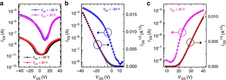
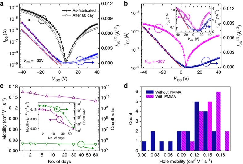
It was reported that Cl might act as a crystallization-retarding and -directing agent60, which benefits the growth of perovskite domains and thus improves the transport properties of the perovskite films21,22. Therefore, we fabricated mixed-halide perovskite CH3NH3PbI3−xClx-based phototransistors. Indeed, we found that the presence of Cl improves the surface smoothness of the perovskite films (Supplementary Fig. 5). The transfer characteristics of the CH3NH3PbI3−xClx-based phototransistor in dark and light conditions are shown in Fig. 4a. Under light illumination (10 mW cm−2), the device shows clear ambipolar behaviour, similar to that of CH3NH3PbI3-based devices. As shown in Fig. 4b,c, the slopes of IDS1/2 versus VGS are linear for a large range of VGS for both p-type and n-type transports, which demonstrates the high quality of our phototransistors. On the basis of equation (1), the obtained mobilities of photo-induced holes and electrons are 1.24 and 1.01 cm2 V−1 s−1, respectively. However, unlike the case of CH3NH3PbI3 phototransistors, IDS in CH3NH3PbI3−xClx devices can reach 10 nA under the dark condition, and the hole and electron mobilities are 1.62 × 10⁻⁴ and 1.17 × 10⁻⁴ cm2 V−1 s−1, respectively (Supplementary Fig. 6). These results obtained under the dark condition imply that the CH3NH3PbI3−xClx channels have substantially higher conductivity and mobility than the CH3NH3PbI3 ones. As shown in Supplementary Fig. 7, the maximum R value of the CH3NH3PbI3−xClx phototransistor is ∼47 A W−1 at VGS=−40 V. The lower R of the CH3NH3PbI3−xClx phototransistor compared with that of the CH3NH3PbI3 phototransistor is primarily because of its higher dark current. Nevertheless, this R value is still comparable to the highest ones reported for other functional materials38,40,42,43,44,45,47,48.
Figure 4. Characteristics of the CH3NH3PbI3−xClx-based phototransistors.
(a) Transfer curves of the CH3NH3PbI3−xClx phototransistor in the dark (black and red symbols) and under light illumination (blue and magenta symbols). (b,c) Representation of the transfer characteristics of p-type and n-type behaviours, respectively, under light illumination.
Characterization of photocurrent response
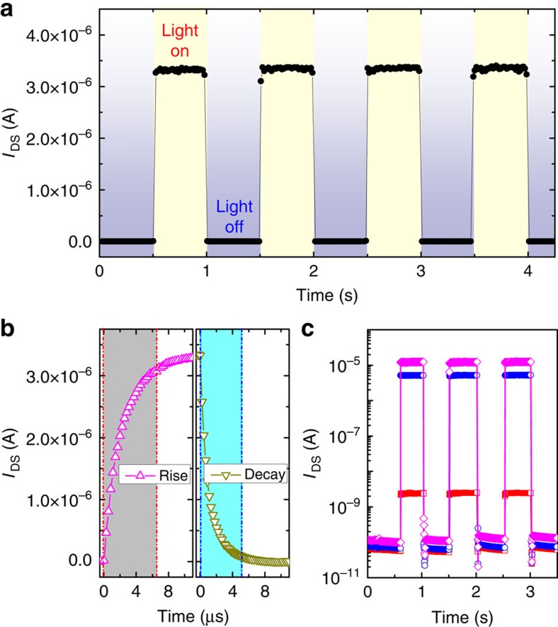
Fast response to optical signals, which is a result of efficient charge transport and collection, is critical for optoelectronic devices. The time-dependent photocurrent was recorded when the white light (10 mW cm−2) was turned on and off regularly. Figure 5a shows the response of photocurrent to optical pulses at a time interval of 0.5 s when the device is biased at VDS=−30 V and VGS=−30 V. We found that the dynamic photoresponse of the perovskite phototransistors was stable and reproducible. The photocurrent quickly increases as soon as the light is turned on and then drops to the original value when the light is turned off, indicating that the device functions as a good light-activated switch.
Figure 5. Photocurrent response of the perovskite phototransistors.
(a) Photocurrent responses of the phototransistors on light illumination showing time-dependent photosensitivity with a time interval of 0.5 s at VGS=−30 V and VDS=−30 V. (b) Temporal photocurrent responses highlighting a rise time of 6.5 μs and a decay time of 5.0 μs. (c) Gate voltage-dependent photoresponses measured at VDS=−30 V. The device was measured at VGS of 0 V (red squares), −30 V (blue circles) and −40 V (magenta diamonds).
Figure 5b shows the temporal photocurrent response of the perovskite phototransistor. The measured switching times for the rise (IDS increasing from 0 to 80% of the peak value) and decay (IDS decreasing from the peak value to 10%) of the photocurrent are ∼6.5 and 5.0 μs, respectively, indicating an ultrafast response speed. The decay time of the photodetector has previously been estimated as the carrier recombination time (lifetime, τlife)39,41,43. Recently, using a solar-cell-type photodetector, Dou et al. obtained response times below 200 ns (ref. 26). In fact, photo-induced electron–hole pairs in the pristine perovskite recombine within a few picoseconds (that is, within the lifetime of the photo-excited electrons)30. However, in the presence of positive (negative) gate voltages, the photo-generated electrons (holes) are accumulated in the channel and acquire a higher mobility, while the other type of charges remain trapped in the perovskite channel. Thus, the recombination of the photo-excited electron–hole pairs in the perovskite channel is reduced, resulting in increased carrier lifetime (τlife)43,61. Nevertheless, the temporal photocurrent responses of our perovskite phototransistors are still substantially faster than those of most organic, quantum dot and hybrid photodetectors (typically in the order of milliseconds)36,41,42,43,44,45,46,47,48,49.
Figure 5c shows the characteristics of photo-switched channel current at VDS=−30 V and various VGS. As shown, on light illumination, a larger VGS can induce a more significant increase in photocurrent. In particular, the photocurrent is ∼2.76 × 10⁻⁹ A at VGS=0 V, whereas it dramatically increases to 1.21 × 10⁻⁵ A at VGS=−40 V. These results demonstrate that the switching of the photocurrent could be tailored to a large degree using the gate voltages, enabling highly tunable photodetection.
Device stability
To enhance the stability of perovskite phototransistors, we coated some bottom-gate top-contact devices with PMMA-protective layers (noted as Device-P). These devices were stored under ambient conditions without isolation from exposures to atmospheric air and moisture. Previous lines of work on perovskite solar cells have demonstrated that coating the PMMA-protective layer is an effective strategy to improve the ambient stability of perovskites by forming kinetic barriers against the diffusion of moisture and/or atmospheric oxygen21. Under light illumination, the transfer curves of a device immediately following fabrication and after storing under ambient conditions for 60 days are essentially the same, except slight decreases in the channel current (shown in Fig. 6a), revealing excellent device stability. In contrast, the unprotected devices without the PMMA layer (noted as Device-U) exhibited sustantially weaker stability. Figure 6b shows the transfer characteristics of a newly fabricated Device-U, which are similar to those of Device-P. The inset of Fig. 6b shows the transfer curve of Device-U that had been stored under ambient conditions for 60 days. Notably, the device showed IDS of only ∼10−8A at VGS=−40 V, which is nearly 104-fold lower than the IDS of the newly fabricated Device-U. Figure 6c shows the mobility and on/off ratio of the Device-P measured at different intervals over a period of 60 days. No apparent statistical variations in the mobilities or on/off ratio were observed, confirming the excellent stability of the encapsulated phototransistors. For the Device-U (shown in the inset of Fig. 6c), both the mobility and the on/off ratio declined continuously during 60 days of storage. However, it should be mentioned that the performance of Device-U changed very little over the first 7 days, indicating that unprotected devices must be measured quickly to achieve reproducible data.
Figure 6. Stability and reproducibility of the perovskite phototransistors.
(a) Transfer curves under light illumination of the Device-P (with the PMMA-protective layer) immediately following fabrication and after storing under ambient conditions for 60 days. (b) Transfer characteristics under light illumination of the as-fabricated Device-U (without PMMA-protective layer). Inset, data measured after storing under ambient conditions for 60 days. (c) Mobility and on/off ratio of Device-P measured during 60 days of storage under ambient conditions. Stability data of Device-U are also shown in the inset for comparison. (d) Histogram of the hole mobilities measured on 20 devices with the PMMA-protective layer and 20 devices without the protective layer.
High reproducibility and stability are critical for photoelectronic devices and their integrations in real-world applications. Figure 6d shows the distributions of hole mobility for both PMMA-protected and -unprotected as-fabricated devices. More than 70% of the Device-P group (20 devices) show hole mobility ranging from 0.13 to 0.19 cm2 V−1 s−1. However, among the 20 devices in the Device-U group, there are notable fluctuations of mobility values: some are similar to Device-P, while others are even below 9 × 10⁻² cm2 V−1 s−1. The perovskite phototransistors without the PMMA layer often exhibit low reproducibility, primarily because of their high sensitivity towards moisture, room light and other factors under ambient conditions. Thus, coating PMMA-protective layers should be considered as a general protocol for enhancing device stability and reproducibility.
Discussion
In this work, ambipolar phototransistors based on solution-processed hybrid perovskites were fabricated and characterized. Owing to the superior optical and electronic properties of hybrid perovskites, our solution-processed phototransistors demonstrated high performances and tunability. Under light illumination, these devices exhibit reliable high performance with balanced carrier mobilities and on/off ratios of ∼104 for both p- and n-type transports. Remarkably, the phototransistors show excellent figures-of-merit such as excellent photoresponsivity (320 A W−1) and ultrafast response speed (less than 10 μs).
In such phototransistors, both light illumination and gate bias can be used to modulate the transport of semiconducting perovskite channels. Through the capacitive coupling, the gate bias is expected to effectively separate the photo-generated holes and electrons, increasing their recombination time, equivalently τlife (ref. 43, 61). The photoconductive gain (G), that is, the number of carriers collected per photo-induced carrier, is given by the equation:
 |
where τtran is the carrier transit time39,41,42,43. For our devices with mobility in the range of 0.2–2.0 cm2 V−1 s−1, G is estimated to be ∼10–102. Through biasing the gate terminal, our phototransistor architecture is advantageous for enhancing the photoresponse.
Furthermore, according to equation (3), the device performance should also benefit from high carrier mobility (μ). In our phototransistors, the field-effect hole/electron mobility was measured as 0.18/0.17 cm2 V−1 s−1 for CH3NH3PbI3 and 1.24/1.01 cm2 V−1 s−1 for CH3NH3PbI3−xClx, this is consistent with the Cl-enhanced electron–hole diffusion lengths observed in previous lines of work on perovskite solar cells21,22. However, better phototransistor performance was achieved in the undoped CH3NH3PbI3 channel as a result of suppressed dark current. We should note that, although the field-effect mobility measured in our perovskite phototransistors is impressive for solution-processed materials, there is still room for improvements. Tailoring the deposition procedures and developing appropriate doping strategies are promising to optimize the transport properties of perovskite channels62,63.
Furthermore, according to equation (3), reducing the channel length (L) is a straightforward way to improve the performance of phototransistors. In the present device structure, the channel length is 50 μm, which are much longer than the diffusion lengths of the carriers. Therefore, light-induced carriers are scattered many times by structural defects and grain boundaries before reaching the electrodes64,65. Much higher carrier mobility is expected in phototransistors with shorter channel lengths, which could further improve the phototransistor performance. Shrinking the channel dimensions may also help decrease the VDS required for the device operation and reduce the energy consumption. Overall, our findings strongly support the use of hybrid perovskites as active materials in high-performance ambipolar phototransistors, and open new doors for employing such solution-processed perovskites in other photoelectronic applications.
Methods
Perovskite preparation and device fabrication
CH3NH3I was synthesized according to a previously reported procedure2,6,11. First, 24 ml of methylamine (33 wt% in absolute ethanol, Sigma) and 10 ml of hydroiodic acid (57 wt% in water, Aldrich) were mixed to react in a 250-ml round-bottomed flask at 0 °C for 2 h with stirring. The precipitate was recovered via evaporation at 50 °C for 1 h. The product, methylammonium iodide CH3NH3I, was washed with diethyl ether by stirring the solution for 30 min, which was repeated three times. The product was finally dried at 60 °C in a vacuum oven for 24 h. The perovskite films were prepared according to the vapour-assisted solution process11. The heavily n-doped Si wafers with 300-nm SiO2 surface layers (capacitance of 15 nF cm−2) were used as the substrates. They were successively cleaned with diluted detergent, rinsed with deionized water, acetone and ethanol and dried with dry nitrogen. After the oxygen plasma treatment, the solution of 0.3 M PbI2 or PbCl2 (Sigma) in dimethylformamide was spin-coated on the cleaned Si substrates at 5,000 r.p.m. for 40 s and dried at 110 °C for 15 min. CH3NH3I powders were spread around the PbI2- or PbCl2-coated substrates, and a Petri dish was placed over the samples. The substrates were heated at 150 °C for 8 h. After cooling, the as-prepared films were washed with isopropanol and dried at 65 °C for 5 min. Finally, Ti/Au (5 nm/80 nm) source (S) and drain (D) electrodes were deposited via thermal evaporation through a shadow mask, defining a channel length (L) of 50 μm and a channel width (W) of 1,000 μm. Furthermore, the fabricated devices were annealed in a glove box at 50–60 °C for 10 min to reduce the charge traps and improve the contact between the active layer and the S/D electrodes66. The bottom-gate bottom-contact devices were fabricated following similar procedures, except that Au S/D electrodes were deposited on the Si substrates before spin-coating the PbI2 or PbCl2 solution. To improve device stability, thin layers of PMMA (average molecular weight ∼350,000 by Gel Permeation Chromatography, Sigma-Aldrich) were spin-coated on the surfaces of the perovskite films at 8,000 r.p.m. for 60 s.
Measurements and experimental set-up
Perovskite film thickness was assessed using the scratch method via AFM (Bruker Dimension ICON). X-ray diffraction patterns of the perovskite films were recorded using a Bruker D8 ADVANCE diffractometer with Cu Kα (λ=1.5406 Å) radiation. A field-emission SEM (FEI Nova Nano 630) was used to acquire surface SEM images. In addition, the morphology of the perovskite films was determined via AFM measurements in the tapping mode. The absorption spectra were measured using an Agilent Cary 6000i UV-Visible-NIR spectrometer. The devices I–V measurements were performed using a Keithley 4200 Semiconductor Parametric Analyzer and a Signotone Micromanipulator S-1160 probe station. A light-emitting diode (white light, 10 mW cm−2) attached to the microscope of the probe station was used as the light source. During the measurements, the samples were kept at room temperature in the ambient atmosphere. The EQE of the device was measured using an Oriel IQE-200 measurement system.
Additional information
How to cite this article: Li, F. et al. Ambipolar solution-processed hybrid perovskite phototransistors. Nat. Commun. 6:8238 doi: 10.1038/ncomms9238 (2015).
Supplementary Material
Supplementary Figures 1-7, Supplementary Table 1 and Supplementary References.
Acknowledgments
This work was supported by King Abdullah University of Science and Technology (KAUST).
Footnotes
Author contributions F.L. performed the device fabrication, data collection and analysis. C.M. assisted in carrying out the film fabrication and characterizations, and W.H. assisted in the device performance measurements. T.W. planned and supervised the project. All authors discussed the results, and prepared and commented on the manuscript.
References
- Kojima A., Teshima K., Shirai Y. & Miyasaka T. Organometal halide perovskites as visible-light sensitizers for photovoltaic cells. J. Am. Chem. Soc. 131, 6050–6051 (2009). [DOI] [PubMed] [Google Scholar]
- Im J.-H., Lee C.-R., Lee J.-W., Park S.-W. & Park N.-G. 6.5% efficient perovskite quantum-dot-sensitized solar cell. Nanoscale 3, 4088–4093 (2011). [DOI] [PubMed] [Google Scholar]
- Kim H.-S. et al. Lead iodide perovskite sensitized all-solid-state submicron thin film mesoscopic solar cell with efficiency exceeding 9%. Sci. Rep. 2, 591 (2012). [DOI] [PMC free article] [PubMed] [Google Scholar]
- Lee M. M., Teuscher J., Miyasaka T., Murakami T. N. & Snaith H. J. Efficient hybrid solar cells based on meso-superstructured organometal halide perovskites. Science 338, 643–647 (2012). [DOI] [PubMed] [Google Scholar]
- Etgar L. et al. Mesoscopic CH3NH3PbI3/TiO2 heterojunction solar cells. J. Am. Chem. Soc. 134, 17396–17399 (2012). [DOI] [PubMed] [Google Scholar]
- Burschka J. et al. Sequential deposition as a route to high-performance perovskite-sensitized solar cells. Nature 499, 316–319 (2013). [DOI] [PubMed] [Google Scholar]
- Zhao Y. & Zhu K. Charge transport and recombination in perovskite CH3NH3PbI3 sensitized TiO2 solar cells. J. Phys. Chem. Lett. 4, 2880–2884 (2013). [DOI] [PubMed] [Google Scholar]
- Heo J. H. et al. Efficient inorganic–organic hybrid heterojunction solar cells containing perovskite compound and polymeric hole conductors. Nat. Photon 7, 486–491 (2013). [Google Scholar]
- McGehee M. D. Materials science: fast-track solar cells. Nature 501, 323–325 (2013). [DOI] [PubMed] [Google Scholar]
- Liu M., Johnston M. B. & Snaith H. J. Efficient planar heterojunction perovskite solar cells by vapour deposition. Nature 501, 395–398 (2013). [DOI] [PubMed] [Google Scholar]
- Chen Q. et al. Planar heterojunction perovskite solar cells via vapor-assisted solution process. J. Am. Chem. Soc. 136, 622–625 (2014). [DOI] [PubMed] [Google Scholar]
- Liu D. & Kelly T. L. Perovskite solar cells with a planar heterojunction structure prepared using room-temperature solution processing techniques. Nat. Photon 8, 133–138 (2014). [Google Scholar]
- Zhou H. et al. Interface engineering of highly efficient perovskite solar cells. Science 345, 542–546 (2014). [DOI] [PubMed] [Google Scholar]
- Weber D. CH3NH3PbX3, ein Pb(II)-system mit kubischer perowskitstruktur. Z. Naturforsch. B 33, 1443–1445 (1978). [Google Scholar]
- Mitzi D. B. In Progress in Inorganic Chemistry 1–121John Wiley & Sons, Inc. (2007). [Google Scholar]
- Kagan C. R., Mitzi D. B. & Dimitrakopoulos C. D. Organic-inorganic hybrid materials as semiconducting channels in thin-film field-effect transistors. Science 286, 945–947 (1999). [DOI] [PubMed] [Google Scholar]
- Stoumpos C. C. et al. Semiconducting tin and lead iodide perovskites with organic cations: phase transitions, high mobilities, and near-infrared photoluminescent properties. Inorg. Chem. 52, 9019–9038 (2013). [DOI] [PubMed] [Google Scholar]
- De Wolf S. et al. Organometallic halide perovskites: sharp optical absorption edge and its relation to photovoltaic performance. J. Phys. Chem. Lett. 5, 1035–1039 (2014). [DOI] [PubMed] [Google Scholar]
- Wehrenfennig C. et al. High charge carrier mobilities and lifetimes in organolead trihalide perovskites. Adv. Mater. 26, 1584–1589 (2014). [DOI] [PMC free article] [PubMed] [Google Scholar]
- Ponseca C. S. et al. Organometal halide perovskite solar cell materials rationalized: ultrafast charge generation, high and microsecond-long balanced mobilities, and slow recombination. J. Am. Chem. Soc. 136, 5189–5192 (2014). [DOI] [PubMed] [Google Scholar]
- Stranks S. D. et al. Electron-hole diffusion lengths exceeding 1 micrometer in an organometal trihalide perovskite absorber. Science 342, 341–344 (2013). [DOI] [PubMed] [Google Scholar]
- Xing G. et al. Long-range balanced electron- and hole-transport lengths in organic–inorganic CH3NH3PbI3. Science 342, 344–347 (2013). [DOI] [PubMed] [Google Scholar]
- Deschler F. et al. High photoluminescence efficiency and optically pumped lasing in solution-processed mixed halide perovskite semiconductors. J. Phys. Chem. Lett. 5, 1421–1426 (2014). [DOI] [PubMed] [Google Scholar]
- Xing G. et al. Low-temperature solution-processed wavelength-tunable perovskites for lasing. Nat. Mater. 13, 476–480 (2014). [DOI] [PubMed] [Google Scholar]
- Tan Z.-K. et al. Bright light-emitting diodes based on organometal halide perovskite. Nat. Nanotechnol. 9, 687–692 (2014). [DOI] [PubMed] [Google Scholar]
- Dou L. et al. Solution-processed hybrid perovskite photodetectors with high detectivity. Nat. Commun. 5, 5404 (2014). [DOI] [PubMed] [Google Scholar]
- Horváth E. et al. Nanowires of methylammonium lead iodide (CH3NH3PbI3) prepared by low temperature solution-mediated crystallization. Nano Lett. 14, 6761–6766 (2014). [DOI] [PubMed] [Google Scholar]
- Dong R. et al. High-gain and low-driving-voltage photodetectors based on organolead triiodide perovskites. Adv. Mater. 27, 1912–1918 (2015). [DOI] [PubMed] [Google Scholar]
- Guo Y. et al. Air-stable and solution-processable perovskite photodetectors for solar-blind UV and visible light. J. Phys. Chem. Lett. 6, 535–539 (2015). [DOI] [PubMed] [Google Scholar]
- Lee Y. et al. High-performance perovskite–graphene hybrid photodetector. Adv. Mater. 27, 41–46 (2015). [DOI] [PubMed] [Google Scholar]
- Chin X. Y., Cortecchia D., Yin J., Bruno A. & Soci C. Lead iodide perovskite light-emitting field-effect transistor. Nat. Commun. 6, 7383 (2015). [DOI] [PMC free article] [PubMed] [Google Scholar]
- Decoster D., Harari J. (eds) Optoelectronic Sensors Vol. 1, Wiley-ISTE (2009). [Google Scholar]
- Sze S. M. & Ng K. K. Physics of Semiconductor Devices Vol. 3, John Wiley & Sons (2007). [Google Scholar]
- Luo H., Chang Y., Wong K. S. & Wang Y. Ultrasensitive Si phototransistors with a punchthrough base. Appl. Phys. Lett. 79, 773–775 (2001). [Google Scholar]
- Ogura M. Hole injection type InGaAs–InP near infrared photo-FET (HI-FET). IEEE J. Quantum Electron. 46, 562–569 (2010). [Google Scholar]
- Liu X. et al. All-printable band-edge modulated ZnO nanowire photodetectors with ultra-high detectivity. Nat. Commun. 5, 4007 (2014). [DOI] [PMC free article] [PubMed] [Google Scholar]
- Avouris P., Freitag M. & Perebeinos V. Carbon-nanotube photonics and optoelectronics. Nat. Photon 2, 341–350 (2008). [Google Scholar]
- Konstantatos G. et al. Ultrasensitive solution-cast quantum dot photodetectors. Nature 442, 180–183 (2006). [DOI] [PubMed] [Google Scholar]
- Konstantatos G. & Sargent E. H. Nanostructured materials for photon detection. Nat. Nanotechnol. 5, 391–400 (2010). [DOI] [PubMed] [Google Scholar]
- Lee J. S. et al. Band-like transport, high electron mobility and high photoconductivity in all-inorganic nanocrystal arrays. Nat. Nanotechnol. 6, 348–352 (2011). [DOI] [PubMed] [Google Scholar]
- Konstantatos G. et al. Hybrid graphene–quantum dot phototransistors with ultrahigh gain. Nat. Nanotechnol. 7, 363–368 (2012). [DOI] [PubMed] [Google Scholar]
- Koppens F. H. L. et al. Photodetectors based on graphene, other two-dimensional materials and hybrid systems. Nat. Nanotechnol. 9, 780–793 (2014). [DOI] [PubMed] [Google Scholar]
- Park S. et al. Significant enhancement of infrared photodetector sensitivity using a semiconducting single-walled carbon nanotube/C60 phototransistor. Adv. Mater. 27, 759–765 (2015). [DOI] [PubMed] [Google Scholar]
- Tang Q. et al. Photoswitches and phototransistors from organic single-crystalline sub-micro/nanometer ribbons. Adv. Mater. 19, 2624–2628 (2007). [Google Scholar]
- Baeg K.-J., Binda M., Natali D., Caironi M. & Noh Y.-Y. Organic light detectors: photodiodes and phototransistors. Adv. Mater. 25, 4267–4295 (2013). [DOI] [PubMed] [Google Scholar]
- Yu H., Bao Z. & Oh J. H. High-performance phototransistors based on single-crystalline n-channel organic nanowires and photogenerated charge-carrier behaviors. Adv. Funct. Mater. 23, 629–639 (2013). [Google Scholar]
- Yin Z. et al. Single-layer MoS2 phototransistors. ACS Nano 6, 74–80 (2012). [DOI] [PubMed] [Google Scholar]
- Zhang W. et al. High-gain phototransistors based on a CVD MoS2 monolayer. Adv. Mater. 25, 3456–3461 (2013). [DOI] [PubMed] [Google Scholar]
- Zhang W. et al. Role of metal contacts in high performance phototransistors based on WSe2 monolayers. ACS Nano 8, 8653–8661 (2014). [DOI] [PubMed] [Google Scholar]
- Zhang F. et al. Ultrathin film organic transistors: precise control of semiconductor thickness via spin-coating. Adv. Mater. 25, 1401–1407 (2013). [DOI] [PubMed] [Google Scholar]
- Meijer E. J. et al. Solution-processed ambipolar organic field-effect transistors and inverters. Nat. Mater. 2, 678–682 (2003). [DOI] [PubMed] [Google Scholar]
- Podzorov V., Gershenson M. E., Kloc C. h., Zeis R. & Bucher E. High-mobility field-effect transistors based on transition metal dichalcogenides. Appl. Phys. Lett. 84, 3301–3303 (2004). [Google Scholar]
- Zaumseil J. & Sirringhaus H. Electron and ambipolar transport in organic field-effect transistors. Chem. Rev. 107, 1296–1323 (2007). [DOI] [PubMed] [Google Scholar]
- Cornil J., Brédas J.-L., Zaumseil J. & Sirringhaus H. Ambipolar transport in organic conjugated materials. Adv. Mater. 19, 1791–1799 (2007). [Google Scholar]
- Fan J. et al. High-performance ambipolar transistors and inverters from an ultralow bandgap polymor. Adv. Mater. 24, 2186–2190 (2012). [DOI] [PubMed] [Google Scholar]
- Bisri S. Z., Piliego C., Gao J. & Loi M. A. Outlook and emerging semiconducting materials for ambipolar transistors. Adv. Mater. 26, 1176–1199 (2014). [DOI] [PubMed] [Google Scholar]
- Snaith H. J. et al. Anomalous hysteresis in perovskite solar cells. J. Phys. Chem. Lett. 5, 1511–1515 (2014). [DOI] [PubMed] [Google Scholar]
- Shao Y. et al. Origin and elimination of photocurrent hysteresis by fullerene passivation in CH3NH3PbI3 planar heterojunction solar cells. Nat. Commun. 5, 5784 (2014). [DOI] [PubMed] [Google Scholar]
- Xiao Z. et al. Giant switchable photovoltaic effect in organometal trihalide perovskite devices. Nat. Mater. 14, 193–198 (2015). [DOI] [PubMed] [Google Scholar]
- Yu H. et al. The role of chlorine in the formation process of “CH3NH3PbI3-xClx” Perovskite. Adv. Funct. Mater. 24, 7102–7108 (2014). [Google Scholar]
- Dutta S. & Narayan K. S. Gate-voltage control of optically-induced charges and memory effects in polymer field-effect transistors. Adv. Mater. 16, 2151–2155 (2004). [Google Scholar]
- Mitzi D. B. et al. Structurally tailored organic−inorganic perovskites: optical properties and solution-processed channel materials for thin-film transistors. Chem. Mater. 13, 3728–3740 (2001). [Google Scholar]
- Mitzi D. B. et al. Hybrid field-effect transistor based on a low-temperature melt-processed channel layer. Adv. Mater. 14, 1772–1776 (2002). [Google Scholar]
- Noel N. K. et al. Enhanced photoluminescence and solar cell performance via Lewis base passivation of organic-inorganic lead halide perovskites. ACS Nano 8, 9815–9821 (2014). [DOI] [PubMed] [Google Scholar]
- Shkrob I. A. & Marin T. W. Charge trapping in photovoltaically active perovskites and related halogenoplumbate compounds. J. Phys. Chem. Lett. 5, 1066–1071 (2014). [DOI] [PubMed] [Google Scholar]
- Gwinner M. C. et al. Simultaneous optimization of light gain and charge transport in ambipolar light-emitting polymer field-effect transistors. Chem. Mater. 21, 4425–4433 (2009). [Google Scholar]
Associated Data
This section collects any data citations, data availability statements, or supplementary materials included in this article.
Supplementary Materials
Supplementary Figures 1-7, Supplementary Table 1 and Supplementary References.


