Abstract
OpenPET is an open source, modular, extendible, and high-performance platform suitable for multi-channel data acquisition and analysis. Due to the flexibility of the hardware, firmware, and software architectures, the platform is capable of interfacing with a wide variety of detector modules not only in medical imaging but also in homeland security applications. Analog signals from radiation detectors share similar characteristics – a pulse whose area is proportional to the deposited energy and whose leading edge is used to extract a timing signal. As a result, a generic design method of the platform is adopted for the hardware, firmware, and software architectures and implementations. The analog front-end is hosted on a module called a Detector Board, where each board can filter, combine, timestamp, and process multiple channels independently. The processed data is formatted and sent through a backplane bus to a module called Support Board, where 1 Support Board can host up to eight Detector Board modules. The data in the Support Board, coming from 8 Detector Board modules, can be aggregated or correlated (if needed) depending on the algorithm implemented or runtime mode selected. It is then sent out to a computer workstation for further processing. The number of channels (detector modules), to be processed, mandates the overall OpenPET System Configuration, which is designed to handle up to 1,024 channels using 16-channel Detector Boards in the Standard System Configuration and 16,384 channels using 32-channel Detector Boards in the Large System Configuration.
Keywords: Electronics, Instrumentation, Nuclear imaging, Open source hardware, Open source software
I. Introduction
The OpenPET [1]–[3] platform provides a flexible and modular data acquisition platform for a variety of applications. This flexibility allows users to interface with different types of detectors. Nowadays, radiation detectors utilize different scintillators (CsI:Tl, NaI:Tl, LSO, GSO, BGO, YAP, etc.) coupled to different photodetectors, such as photomultiplier tubes (PMTs), position-sensitive PMTs, multianode PMTs, PIN photodiodes, avalanche photodiodes (APDs), position-sensitive APDs, hybrid photodetectors, and silicon photomultipliers (SiPMs). Additionally, solid-state detectors such as silicon, high-purity germanium (HPGe), and cadmium zinc telluride (CZT) are also commonly used as radiation detectors. The output signals from these detectors share similar characteristics and can be combined in multiple ways depending on the application and purpose: Simple (individual coupling and four channel “block detectors”) to moderately complex (Anger cameras that read out dozens of PMTs and row/column readout) to complex (position-sensitive detectors on both ends of a scintillator crystal array). It is also possible to have setups that use an array of photosensors to infer the three-dimensional location of an interaction inside a given crystal. Even though there are different variations of radiation detectors, the analog signals from most detectors are very similar i.e. a pulse whose area is proportional to the deposited energy and whose leading edge is used to extract timing.
A. System Configurations and Capacities
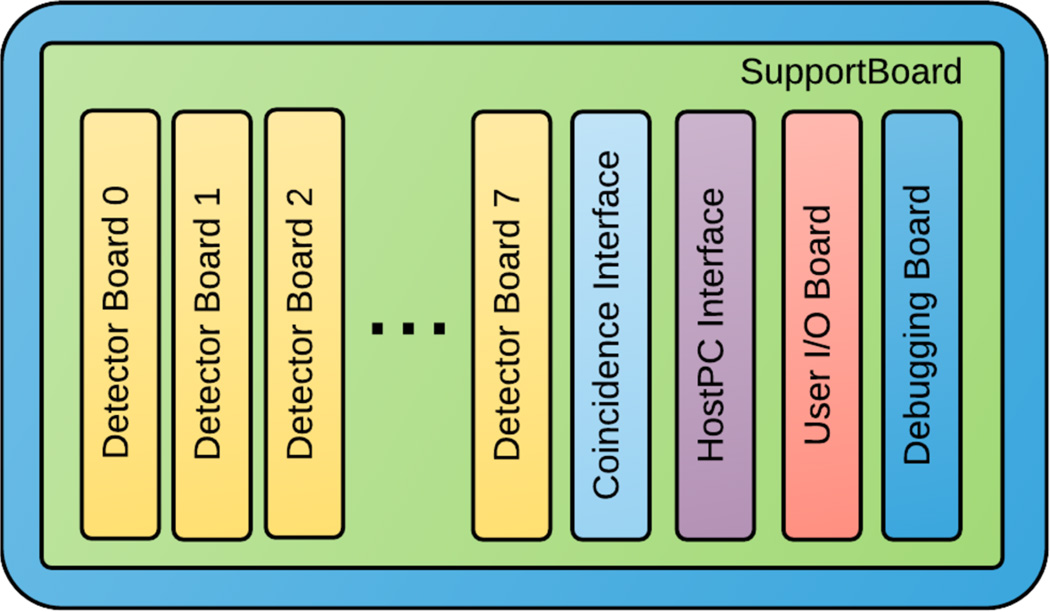
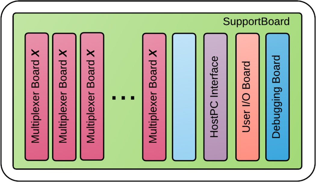
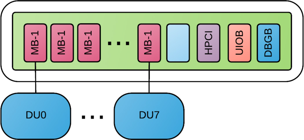
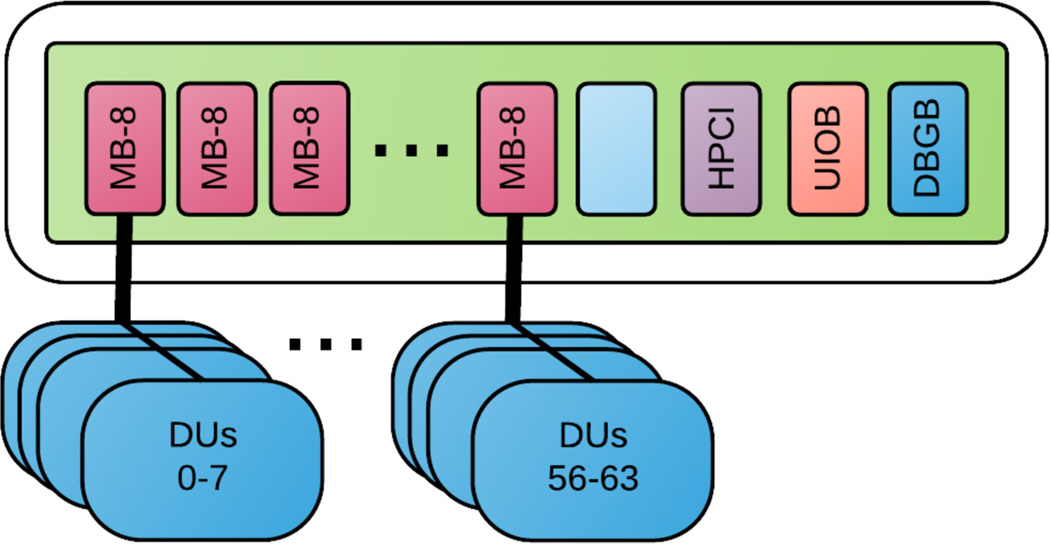
OpenPET offers three system configurations: a Small System (a single Detector Unit), depicted in Fig. 1, which is capable of capturing and processing up to 8 Detector Boards, a Standard System, shown in Fig. 2 and Fig. 3, up to 64 Detector Boards, and Large System, displayed in Fig. 4, up to 512 Detector Boards.
Fig. 1.
Small System Configuration (a single Detector Unit). The first 8 slots in the chassis are populated with Detector Boards, which are connected directly to the detector’s analog signals. The ninth slot is a Coincidence Interface Boards which allows the system to be expanded to a Standard Configuration or a Large Configuration.
Fig. 2.
Coincidence Unit. The only difference between a Coincidence Unit and a Detector Unit (shown in Fig. 1) is that the first eight slots in the chassis are populated with Multiplexer Boards instead of Detector Boards and the 8th slot is not populated with the Coincidence Interface Board.
Fig. 3.
Standard System Configuration. A single Detector Unit (DU) (shown in Fig. 1.) is connected (through a Coincidence Interface board) to a single passive, no active components, Multiplexer Board (MB-1) in a Coincidence Unit (shown in Fig. 2). Therefore, up to 8 Detector Units can be connected in this configuration.
Fig. 4.
Large System Configuration. eight Detector Units (shown in Fig. 1.) are connected (through Coincidence Interface boards) to a single active, FPGA based, Multiplexer Board (MB-8) in a Coincidence Unit (shown in Fig. 2). Therefore, up to 64 Detector Units can be connected in this configuration.
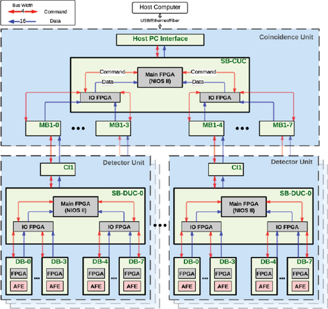
In this paper, we will mainly focus on the Standard System, depicted in Fig. 5, which consists of a maximum of 8 Detector Units (DU), where a DU is a Support Board (SB) module mounted as a backplane on a standard 12-slot 6U VME chassis. A DU's SB can host up to 8 Detector Boards (DBs). A DB is designed to process multiple analog detector signals. For example, a Standard System can support a maximum of 1024 channels using a 16-channel DB (16 analog channels per DB, 8 DBs per DU, and 8 DUs). Alternatively, it supports a maximum of 2048 detector signals when using a 32-channel DB.
Fig. 5.
Simplified Standard System architecture. An analog detector signal is passed through the analog front end (AFE) for filtering, timestamping, and digitization. Then it is processed using real-time algorithms on the DB’s FPGA and handed over to an IO FPGA for multiplexing. Finally it is given to the main FPGA for correlation and combination. A DU packs the formatted data and passes it to its parent chassis.
B. Expected System Performance
The architecture is designed to be high-performance in order to serve the new generation of radiation detection data acquisition systems. Some of the important performance metrics are a large number of channels, i.e., up to 16,384, high maximum count rate (>106 singles events/second), good energy resolution (<2% fwhm for test pulses), and good timing resolution (<1ns fwhm for conventional PET, <100 ps fwhm for time-of-flight PET).
C. Data and Control Flow
Using a bottom-top approach on Fig. 5, analog signals coming from a detector is passed through the analog front end (AFE) on the DB. The signal is divided into two paths; one to compute the energy and the other to compute the timing. For example, considering the energy path on the OpenPET 16-channel Detector Board module [2], the analog signals are amplified and trimmed using an anti-aliasing filter with a 3dB cutoff frequency in the range of 6.5 MHz to 10 MHz. The filtered signal is fed to a 12-bit pipeline analog-to-digital converted (ADC) and can be sampled at a rate between 10 MSPS to 65 MSPS. For the timing path, the signal is amplified with a ×10 high-bandwidth amplifier and then passed to a fast comparator to trigger on the leading edge of the analog signal.
The digitized data and the generated pulse from the timing comparator are fed to the FPGA for further processing. The digitalized data is processed using user defined real-time algorithms. The timing pulse is fed to a time-to-digital converter (TDC) soft core [4] to determine the arrival timestamp of the analog signal.
The data is combined (and correlated if needed), multiplexed, and formatted by the Support Board Detector Unit Controller (SB-DUC), which defines the SB loaded with the detection firmware. The data from the DB is sent out to the SB IO FPGA for additional processing and correlation, if required. The processed data is then passed to the SB Main FPGA. The Main FPGA on the SB-DUC combines and multiplexes the data out. For a Small System, the data is passed to a Computer Workstation for offline processing, using USB or Ethernet. For a Standard System further multiplexing and processing occurs where the formatted data is passed to a Coincidence Interface Board (CI) that is plugged into the SB. This CI board simply passes the data, through a shielded, cable to a Multiplexer Board (MB) that is plugged into a Coincidence Unit (CU). A CU is essentially a DU with MBs plugged into the slots where DBs reside as shown in Fig. 2. The MB passes the formatted data from the CI board to the Support Board Coincidence Unit Controller (SB-CUC), which defines the SB loaded with the coincidence firmware. The SBCUC will do the final processing (e.g., finding the coincidence event, formatting the coincidence word, etc.) of the data coming from all the DUs and then send final data (via USB or Ethernet) to a workstation for storage or offline processing.
The command and control flow is similar to the data flow; however, the commands are initiated from top-to-bottom, similar to a tree topology. On startup, each node in the tree discovers its parent and children, and all addresses are configured accordingly. A user (or a script) initiates a command from the workstation. This command will be translated and encoded to the corresponding child, i.e., SB-CUC. Consecutively, each node will pass the command to its corresponding child(ren) by looking at the destination address. Finally, once the command reaches its desired destination(s) the corresponding node(s) execute(s) the command and send(s) a reply, if required.
II. Architecture and Implementation
A. Clock Distribution
In OpenPET there are two main clocks: CLK and Slice. The former represents the main clock source and it is sourced from an 80 MHz local oscillator or fed from an external SMA connector with a frequency range of 5 – 400 MHz. On the other hand, Slice, also known as frame clock, is a slower frequency clock and behaves similar to ADC frame clocks, i.e., it wraps X number of clock ticks to represent a “Word”. When the main CLK is 80 MHz the Slice is typically 1/8th or 1/16th of that frequency, which translates to 10 MHz or 5 MHz respectively. Additionally, it is important to mention that sometimes it might be desirable to create a “valid” signal instead of a periodic Slice (frame) clock; therefore, the Slice signal is thought of as a dual purpose clock/signal depending on the mode of operation in the firmware. For example, in Scope mode, discussed in section E.1), the firmware does not require a periodic Slice clock. As a result, a “valid” is used there.
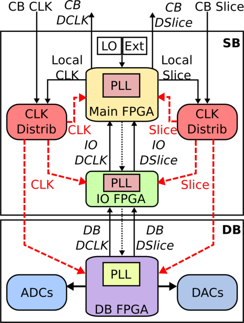
The uppermost node is responsible for generating the CLK. OpenPET provides two methods: (a) a Local Oscillator (LO) running at 80 MHz or (b) an External clock (Ext) fed through a dedicated SMA connector. Fig. 6 shows a simplified clock topology of the entire system. All clocks are distributed using LVDS and are fed to clock capable pins on the FPGAs. Each FPGA in the system utilizes an internal Phase-Locked-Loop (PLL) in order to keep all components of its system synchronized. The lowermost unit (Detector Unit) in a Large or Standard System Configuration receives CLK and Slice through the Coincidence Interface Board and passes them separately to two dedicated very low jitter and skew clock distribution ICs (TI CDCLVD110) as shown in Fig. 6. For CLK, the clock distribution IC generates ten replicas: one goes to the Main FPGA on the Support Board, one goes to the two IO FPGAs on the Support Board (the second IO FPGA is not shown in figure for simplicity), and eight go to the first 8 slots in the chassis targeting DBs or MBs. Note that the clocks in Fig. 6 are connected on Detector Boards, but the concept is the same for Multiplexer Boards.
Fig. 6.
Clock topology of OpenPET. The clock source in the entire platform depends on the system configuration. For a Large and Standard System Configurations the main clock source is a local oscillator (LO) or an external clock source (Ext) on the Support Board in the upper most node. This clock propagates down through the Coincidence Interface Board (CB CLK) to a dedicated clock distributed IC (Integrated Circuit) chip. Then it is fed to the PLLs in the Main FPGA and IO FPGAs on the Support Board as well as the PLL in the Detector Board or Multiplexer Board FPGA. Clocks which have a direction from top to bottom are generated by the uppermost node and used in all children. Clocks which have a direction from bottom to top are PLL clocks synchronized with the parent node and their purpose is to clock the data from the lowermost node to the uppermost parent. The dotted unlabeled clock is a low speed serial clock for commands and control.
The internal PLLs do not only synchronize the timing across multiple system components but also serve as a standard design block shared across multiple boards and FPGAs. This standardization helps simplify the overall firmware architecture by reusing the same blocks of code across different nodes. For example, the reset logic in the entire platform depends on the PLL locking to CLK. Therefore, the reset code is reused across all nodes.
The PLL core in the uppermost parent generates 4 clocks: (i) Main system clock (typically running at 80 MHz) is used to feed the clock distribution IC in order to clock all components in the system. It also clocks all FPGA modules i.e., Altera’s Qsys module which contains the NIOS soft core microprocessor, QuickUSB logic, and the generic Software-Firmware Interface module. (ii) Data path clock (typically running at half the frequency of the main system clock) is used to transfer the clock domain of the incoming children data/clock to the system clock domain. (iii) Frame or slice clock is a slow clock which feeds another clock distribution IC in order to align all components in the system. The rising edge of this clock is used to create a synchronized startup pulse in the entire system. However, the main use of this clock is to wrap or frame the data in all children in fixed time intervals, i.e., simplify pipelining the data as well as define event boundaries for coincidence computations. (iv) QuickUSB clock (typically running at 30 MHz but can be between 5 – 48 MHz) is used to clock data out of OpenPET chassis to a workstation. It is also used to clock in user commands from the workstation to the OpenPET system.
Moreover, in all other nodes (e.g., DBs) in the system the PLL core generates 2 clocks: (i) Main system clock (typically running at 80 MHz) is a clock signal derived from the clock distribution IC found in the node’s parent. Its main purpose is to clock all FPGA modules, i.e., Altera’s Qsys module which contains the NIOS soft core microprocessor. It is also used to clock the generic Software-Firmware Interface module. (ii) Data path clock is used to clock all external components (e.g. ADCs and DACs) as well as transfer the acquired data from ADCs clock domain to the child’s output stage clock domain.
B. FPGAs and Other Peripherals
To simplify the hardware and firmware development, all FPGAs in the OpenPET platform share the same part number Altera Cyclone III EP3C40F780C7. This facilitates easier Printed-Circuit-Board (PCB) design and fabrication as well as lowers the overall cost of the platform by reusing the same parts. Additionally, it helps firmware engineers to reuse blocks of code across different OpenPET components.
In order to seamlessly program and update the firmware in a given OpenPET node, the Main FPGA in the Support Board is connected to a 64Mb Flash memory device for Active Serial Configuration called “EPCS64.” OpenPET stores all firmwares (total of three) as well as the embedded software (for NIOS) in a single EPCS device on the Support Board.
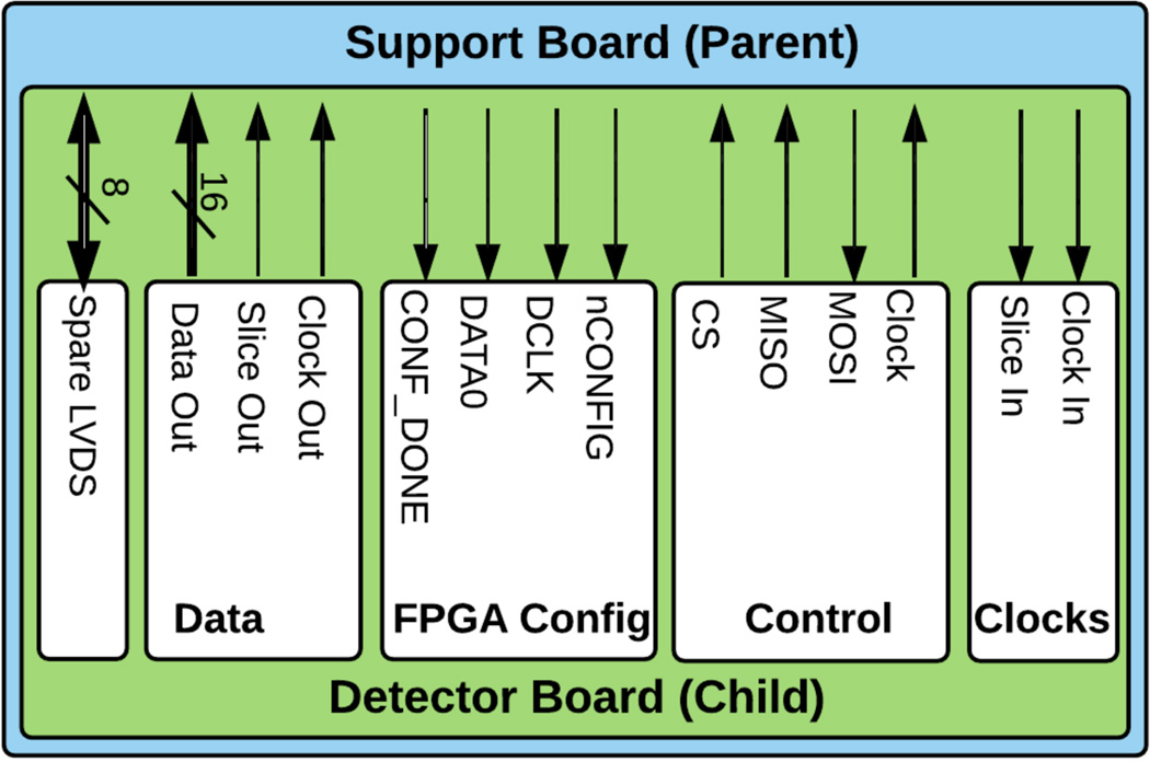
On power up, the Main FPGA loads its compressed firmware as well as its embedded software from the EPCS. After that the compressed firmware and embedded software images of the two IO FPGAs on the Support Board are loaded. Once the IO FPGAs are programmed and running, the embedded software in the Main FPGA, by default, programs all children (e.g., DBs) using the Passive Serial Configuration Interface, shown as “FPGA Config” in Fig. 7, with an uncompressed firmware/embedded software image that is also stored in the EPCS. This default behavior helps to bring up a working system in the shortest amount of time with the least amount of effort. Note that if we use a compressed image for children nodes (e.g. DBs), the bitstream size will be unknown (i.e. variable), which requires the end-user to modify and rebuild the firmware and embedded software of the SB whenever a change occurs on the Detector Board firmware or software. Therefore, we sacrifice the extra space used by an uncompressed image for the sake of flexibility and user friendliness.
Fig. 7.
Backplane I/O communication bus. A single child is shown in the figure for simplicity. The Support Board can host up to eight children. From right to left: the main clocks incoming from parent (LVDS), SPI interface (Single-Ended), Altera Passive Serial FPGA configuration (Single-Ended), outgoing data and clocks (LVDS), and bi-directional signals (LVDS).
Finally, other peripherals like LEDs, SRAM, temperature sensors, and Logic Analyzer debugging headers are available in all components of the system for debugging purposes, user friendliness, and flexibility. For example, SRAM memory provides a useful storage for different uses like DAC thresholds, calibration coefficients, lookup tables, etc.
C. Overview of I/O Communications
1) Host Workstation PC to OpenPET interface
Currently, there are two methods to communicate with an OpenPET system: (a) using BitWise QuickUSB module [5] or (b) using Gigabit Ethernet 1000BASE-T (copper) or 1000BASE-X (fiber). Both options allow for full-duplex communication between a workstation and OpenPET.
QuickUSB uses USB v2.0 which supports up to 480Mbps transfer rates. QuickUSB provides two clocking schemes: internal and external. OpenPET uses the latter which means that QuickUSB does not internally generate a clock, but it accepts an external clock generated from the Main FPGA on the Support Board. This scheme mandates that all commands and data from OpenPET to QuickUSB (or vice versa) are synchronized to the main clock source described in subsection A above. In return, it simplifies firmware development and timing constraints as well as provides better data integrity by using a PLL output clock to sample the data.
Gigabit Ethernet requires an additional module in the OpenPET platform called Host PC Interface Board. This board is plugged into the tenth slot in the chassis, as shown in Fig. 1, and uses a dedicated PHY chip for the gigabit transceiver. The maximum theoretical transfer rate of Gigabit Ethernet is 1250Mbps; however, this rate depends on the way the Ethernet subsystem is implemented in firmware. For example, for a simple software implementation (e.g. using a NIOS microprocessor, Direct Memory Access (DMA), and a soft User Datagram Protocol (UDP) stack), this metric is reduced by approximately 20% – 40%. On the other hand, using a custom firmware with NIOS, hardware offloading, and modular Scatter-Gather Direct Memory Access (SGDMA), the transfer rate can achieve 90% to 99% of its maximum capacity [6].
2) Inter OpenPET interfaces
OpenPET modules and components have two separate links for data path and control path. This is depicted in Fig. 7.
The data path uses sixteen LVDS pairs (shown as Data sub-block in Fig. 7) to transfer large amounts of data, e.g. ADC samples from one child to its parent. The data is clocked out using “Clock Out” pins in the same sub-block in the figure. This clock is generated using an internal PLL whose input clock is “Clock In” (shown as Clocks sub-block in Fig. 7.) An additional LVDS bus (eight pairs) is also available for applications that require more than sixteen IO data lines.
The control path, on the other hand, uses four single-ended lines, which are currently used to implement a standard Serial Peripheral Interface (SPI). The Control sub-block in Fig. 7 shows the four signals: “Clock” which is a slow frequency serial clock, “MOSI” is a master output slave input port, “MISO” is a master input slave output port, and “CS” is chip select. It is worth mentioning that these 4 signals can be used to implement other serial protocols instead of SPI. However, a custom firmware and embedded software interface must be implemented in all nodes replacing the current SPI implementation described in the sections below.
D. Command and Control flow
All commands are initiated by the user on a workstation. A script or a Graphical User Interface (GUI) program is used to transfer the commands from the workstation to the OpenPET chassis via a QuickUSB module or an Ethernet port on the PC Interface Board. Ethernet packets are passed directly to the NIOS for further processing, however, when using QuickUSB an intermediate firmware module relays the commands from the workstation via FPGA fabric to the NIOS microprocessor using a First-In-First-Out (FIFO) memory module.
After a command is received by the parent node, it is processed by its NIOS microprocessor and a reply (response) is constructed and sent back to the original sender.
All command and reply packets are designed to have the same length. The current command length in the OpenPET platform is 80-bits (i.e., 10 bytes) as shown in Fig. 8. However, this length is generic by design; in other words, a user can easily change the default length of the OpenPET command by changing a single variable called “CMD_PKTS” in the firmware and software. This feature gives the user greater flexibility in their implementation, and it provides a paved roadmap for future extensions of the OpenPET platform. Note that due to a restriction imposed by the QuickUSB module and SPI bus widths, the commands/replies have to be a multiple of 16-bits e.g. 80, 96, 112, 128 bit, etc.
Fig. 8.
Command or Reply packet in OpenPET where the command length is defined to be 80-bits. CMD ID: 1-bit c/r flag + 15-bit command identifier. SRC Addr: is a 16-bit address field stating the packet has originated from. DST Addr: 16-bit address field stating the packet’s target. Payload: 32-bit value that contains arbitrary data related to the command or the reply.
The command identifier (CMD ID in Fig. 8) is a 16-bit value where the most significant bit (MSB) (named in this context as c/r flag) is used as a multi-purpose flag: (a) when the uppermost parent sends down a command with this flag set to 0 (default behavior), the destined child is expected to execute the command (identified by the remaining 15-bits) and send a reply within a pre-defined timeout period (typically 200 ms). If the reply is received the parent will be satisfied; however, if no reply is received, the parent will attempt to send the same command X number of times before coming to a conclusion, i.e., busy child, dead child, out of memory, etc. The number of retries X is a constant defined in the client’s software and NIOS embedded software in all nodes. (b) When the child responds back to a command after a successful execution, it sets the c/r flag to ‘1’ (default behavior). (c) When the uppermost parent sends down a command with this flag set to ‘1,’ this command is considered asynchronous, or, non-blocking. A non-blocking command becomes useful when a child or a grandchild requires a lot of time (more than the permitted timeout period and retries) to complete a task. For example, a child is waiting for a user to press a button, or a DAC is sending a train of pulses to a detector board for a long period of time. The first child that receives a non-blocking command replies immediately to the parent acknowledging that it has received the command. Then it either executes the command or passes it down to its destination.
The address field (SRC Addr or DST Addr in Fig. 8) are 16-bit fields where each bit or ranges of bits are defined as shown in Fig. 9. The Broadcast flag bit is used only when sending a command and it causes the first receiving child to broadcast the command to all grandchildren. MBC, CDUC, CUC, and DUC flags are 1-bit flags used when sending a command to a specific chassis controller. The HostPC flag indicates that the source or the destination is the workstation.
Fig. 9.
16-bit Address field: From MSB, Boardcast flag, HostPC flag, not used, Multiplexer Board Controller flag, Coincidence and Detector Unit Controller flag, Coincidence Unit Controller flag, Detector Unit Controller flag, 3-bit Multiplexer Board address, 3-bit Detector Unit address, and 3-bit Detector Board address.
E. Data Flow
In order to support different DBs with a different number of channels, there is a need to create a generic source synchronous ADC interface. OpenPET utilizes Altera’s Cyclone III FPGA which does not come with a dedicated SERDES (serializer/deserializer) circuit; therefore, the generic interface has to be implemented in FPGA fabric without relying on any dedicated or integrated high-speed interfaces. This introduces a challenge because the number of resources (PLLs, Lookup tables, etc) are limited and shared with other modules in the DB. As a result, a parameterized compact design is implemented to allow OpenPET to interface a wide range of pipeline ADC with maximum sampling frequencies of approximately 250 MHz +/− 50 MHz. The design utilizes a standard Altera core called “DDIO” which supports double data rate I/O in order to clock the incoming ADC data at both rising and falling edges without using any additional PLL cores.
1) Scope Mode (Raw Data)
Oscilloscope or Scope mode is a system data mode where ADC samples are transferred as-is from the DBs all the way to the workstation. The user must correctly configure the settings of this mode to get meaningful data. To use this mode, the user has to send the command ID “SET_SYS_DATA_MODE” with a payload of 0×1, followed by the command ID “SET_SYS_DATA_MODE_SETTINGS” with the proper payload as shown in Fig. 8. Finally the user can run it by sending the command ID “SET_SYS_DATA_MODE_ACTION” with a payload of 0×1. Once the correct configuration is in place data transfers are activated by a trigger, e.g. an incoming analog signal whose pulse height is larger than a predefined DAC threshold. When the acquisition starts, 32-bit packets from different channels, detector boards, or detector units are simply transferred sequentially using a round-robin scheduling algorithm. All complex sorting operations are deferred to a later stage, i.e., the workstation, in order to keep the firmware architecture simple, small, and predictable.
As described above, Scope mode settings allow the user to set run-time configurations. These settings are shown in Fig. 10 and briefly described hereafter. The 32-bit payload contains four main parameters: (i) a 4-bit Data Format sets the output format of the Scope mode. (ii) A 9-bit Number of Samples specifies the number of samples to stream. (iii) A 4-bit Number of Samples Before trigger specifies how many samples the firmware has to buffer before a trigger occurs. (iv) A 4-bit Trigger Window specifies the number of samples to monitor on all channels after a trigger occurs on one channel. If any other channel triggers during this time, its header will also have the ‘triggered’ bit flag set to ‘1’.
Fig. 10.
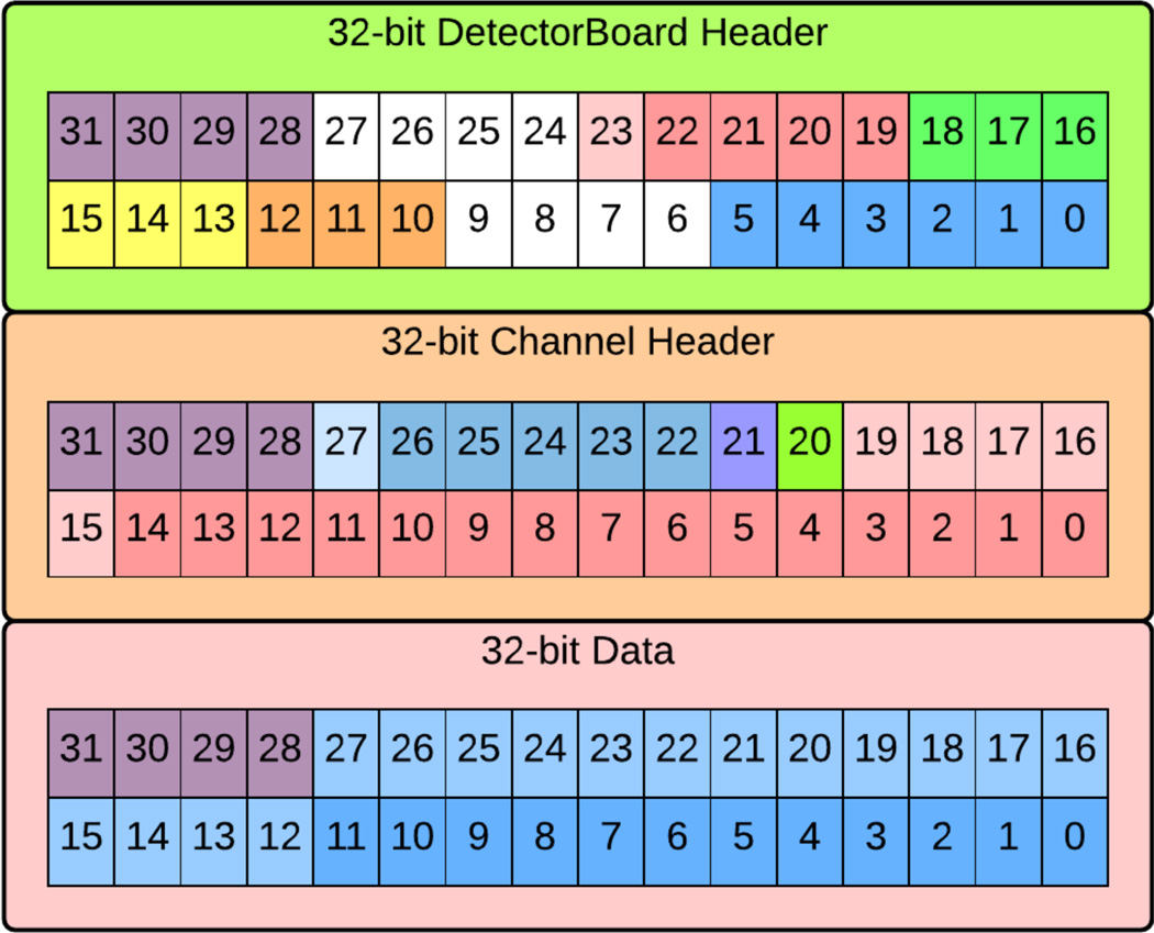
Data path headers and samples for Scope Mode. Detector Board header starting at LSB: (5:0) Number of channel header packets, (9:6) not used, (12:10) Detector Board Address, (15:13) DUC Address, (18:16) MB Address, (23:19) Data Format, (27:24) not used, (31:28) Packet ID (must equal to 0×4). Channel Header starting from LSB: (19:0) TDC data (if used), (20) hardware trigger hit (energy), (21) firmware trigger hit, (27:22) channel address, (31:28) Packet ID (must equal to 0×3). ADC data sample starting from LSB: (27:0) e.g. raw ADC data from (11:0), (31:28) Packet ID (must equal to 0×1).
The data transferred from all detector boards is fairly transmitted through the use of the round-robin scheduling algorithm at the SB stage. Hence, a 32-bit channel header and a 32-bit detector board header, depicted in Fig. 10, are inserted in the data path stream. It is also crucial to assign a 4-bit packet ID to differentiate channel headers, detector headers, and ADC data samples packets; thus, the four most significant bits of the 32-bit data packets are dedicated to that purpose. For example, bits (31:28) for a channel header must have a value of 0×3, a detector board header must have a value of 0×4, and the value for an ADC data sample must be 0#x000D7;1.
2) Other modes (e.g. singles, coincidence)
Singles mode is a system data mode where ADC samples are processed on the Detector Board to create a Singles Event Word (SEW), which is a digital representation of a single gamma ray interaction. These SEWs are passed to the SB-DUC whose main function is to multiplex the SEWs from multiple Detector Boards. The multiplexed SEWs are then passed to the SB-CUC. The SB-CUC searches through the SEWs for pairs that are in time coincidence and form a Coincidence Event Words (CEWs). These CEWs are then passed to the workstation. Optionally, the SB-CUC can act as a multiplexer and just pass unaltered SEWs to the workstation.
The system divides time into small, fixed length time slices depending on the CLK and Slice ratio (e.g.100–200 ns or 8–16 clocks when CLK is 80 MHz and Slice is 10 or 5 MHz.) All individual operations must occur within a single Slice period, which implies that only single event words that occur in the same Slice period can be combined to form a coincident event. Since it can take a significantly longer time than a single Slice period to process one event, the system is designed to pipeline operations so that the processing is divided into smaller steps that each can be completed in a single Slice period. The SEWs are output using the 16-bit wide data bus as shown in Fig. 7. By grouping these 16 lines into 4 sets of 4 lines each, the SEWs can be 64-bit or 128-bit long with 8 clocks (100 ns) or 16 clocks (200 ns) of the system CLK respectively. During one Slice period, boards that output SEWs (e.g., the DBs and CI boards) can pass up to 4 SEWs. Thus, the maximum singles rate that can be transferred to the SB-DUC is 32 SEWs (four for each of the eight DBs) per Slice period. The SB-DUC can multiplex a maximum of 4 SEWs to the SB-CUC. Similarly, SB-CUC can receive a maximum of 4 SEWs from each of the 8 DUs in the Standard System to form the CEWs in the SBCUC. In practice, the maximum event rate is limited by the transfer rate between the SB-CUC and the workstation, which is considerably slower, i.e., a maximum throughput of 480 Mbps for QuickUSB and 1 Gbps for gigabit Ethernet.
III. Embedded Software
Embedded software uses plain C, and runs on Altera’s embedded soft core NIOS microprocessor. The subsections below describe the major building blocks of the embedded software.
A. NIOS
All FPGAs in the OpenPET system contain a NIOS processor. On the Main FPGA in the SB, the NIOS processor has extra features enabled like caching, larger memory space, CPU debugging, etc. On the other hand, the NIOS processors running in the IO FPGAs in the SB and DB utilize a minimal NIOS core to keep the implementation size minimal.
Having NIOS in all FPGAs simplifies the design and development of the firmware as well as the embedded software. For example, in the firmware development, the Software-Firmware Interface module is reused in the Main and IO FPGAs in the SB and in the DB FPGA. Additionally, in the embedded software the SPI interface is reused in all FPGAs as well. In addition to the two benefits mentioned above, this method simplifies the testing and enhances the stability of the developed reusable block.
Finally, having NIOS in all FPGAs requires bundling the embedded software along with the firmware in order to create a single bitstream image. However, this requires the use of the scarce on-chip FPGA memory when DDR memory is not available, i.e., IO FPGAs and DB FPGAs. As a result, this restricts the embedded software size to be very small (e.g. less than 10 KB) so that the embedded software will fit in an onchip memory without taking many resources from the rest of the FPGA fabric.
B. SPI Interface for Commands and Control
In order to keep a standard design throughout the platform, OpenPET uses Altera’s standard 32-bit SPI core to generate the firmware interface and Altera’s standard SPI hardware abstraction layer (HAL) and application program interface (API) library for the embedded software.
Since the length of an OpenPET command is variable as described in Section II.D the SPI interface has to be flexible to allow us to accommodate any expansion or future improvements. As a result, a modular SPI software interface is implemented to convert QuickUSB and Ethernet commands to 32-bit SPI transactions.
For any given command, it is important to transfer the command ID as well as the payload to the destined child; therefore, the parent of the destined child will be responsible for managing the source and destination addresses of the OpenPET command. For example, in the default 80-bit command implementation of OpenPET, two 32-bit SPI transactions will occur: The first transaction will contain the 16-bit command as well as 16-bit source address. The second transaction will contain the 32-bit payload. Note, that the parent dropped the source address from the command because it is not needed by the child but it will include it back when it replies.
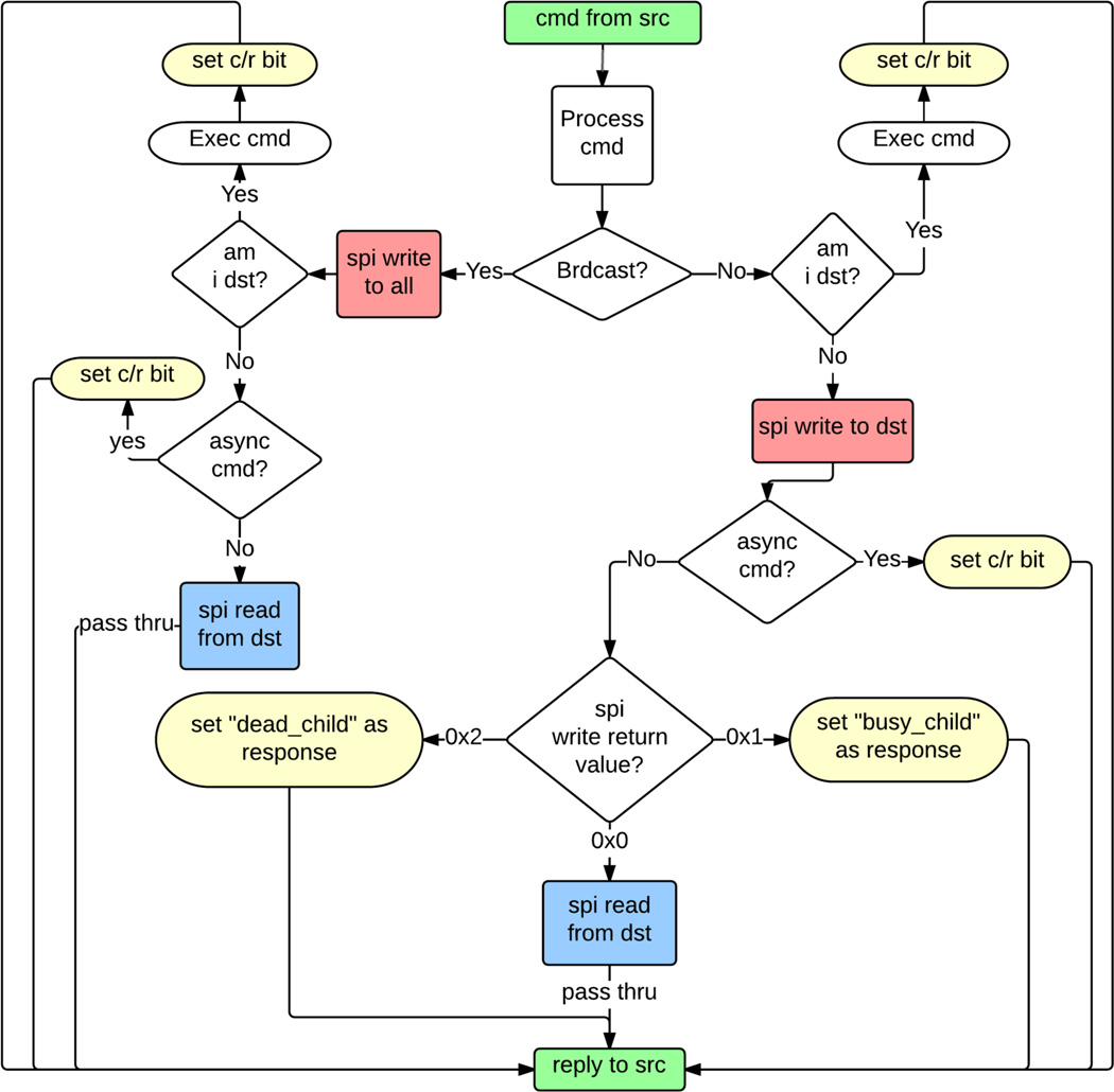
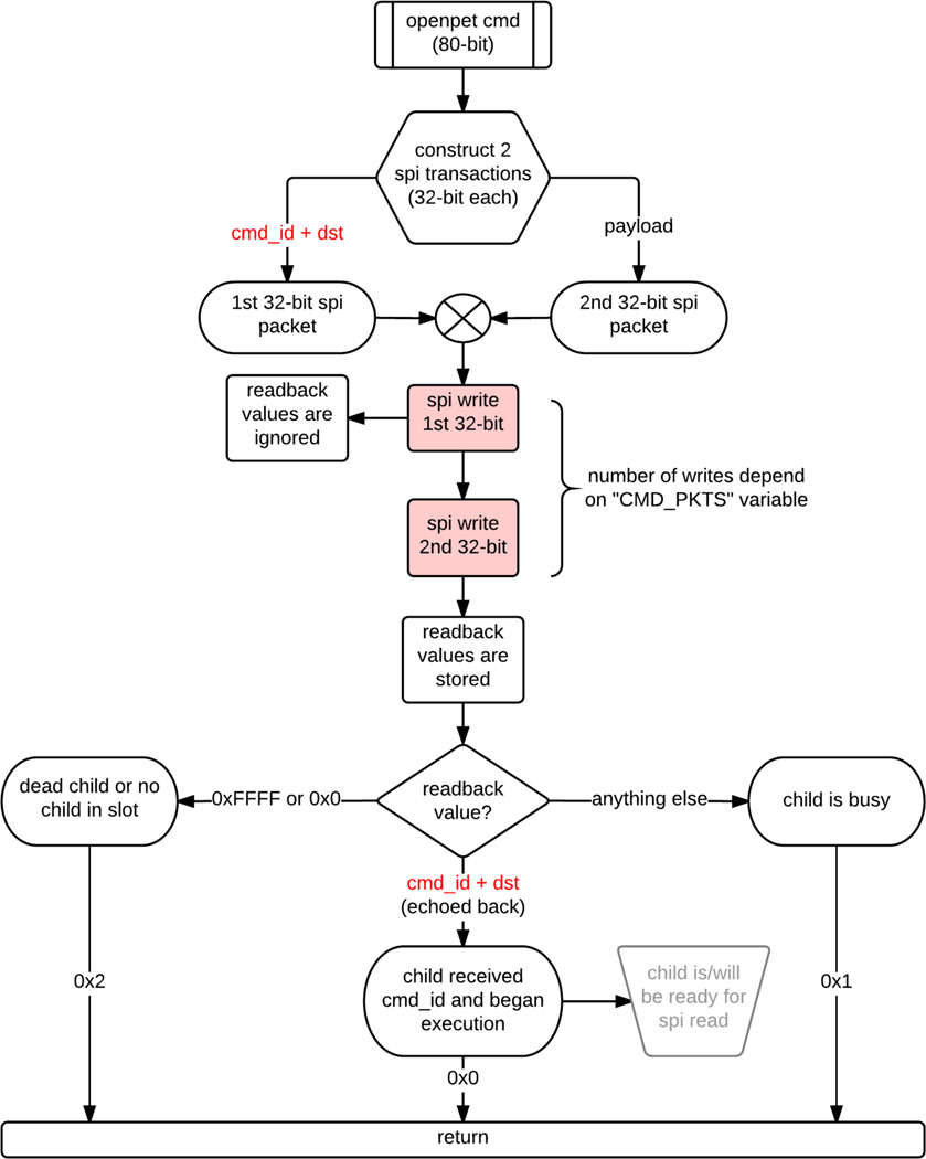
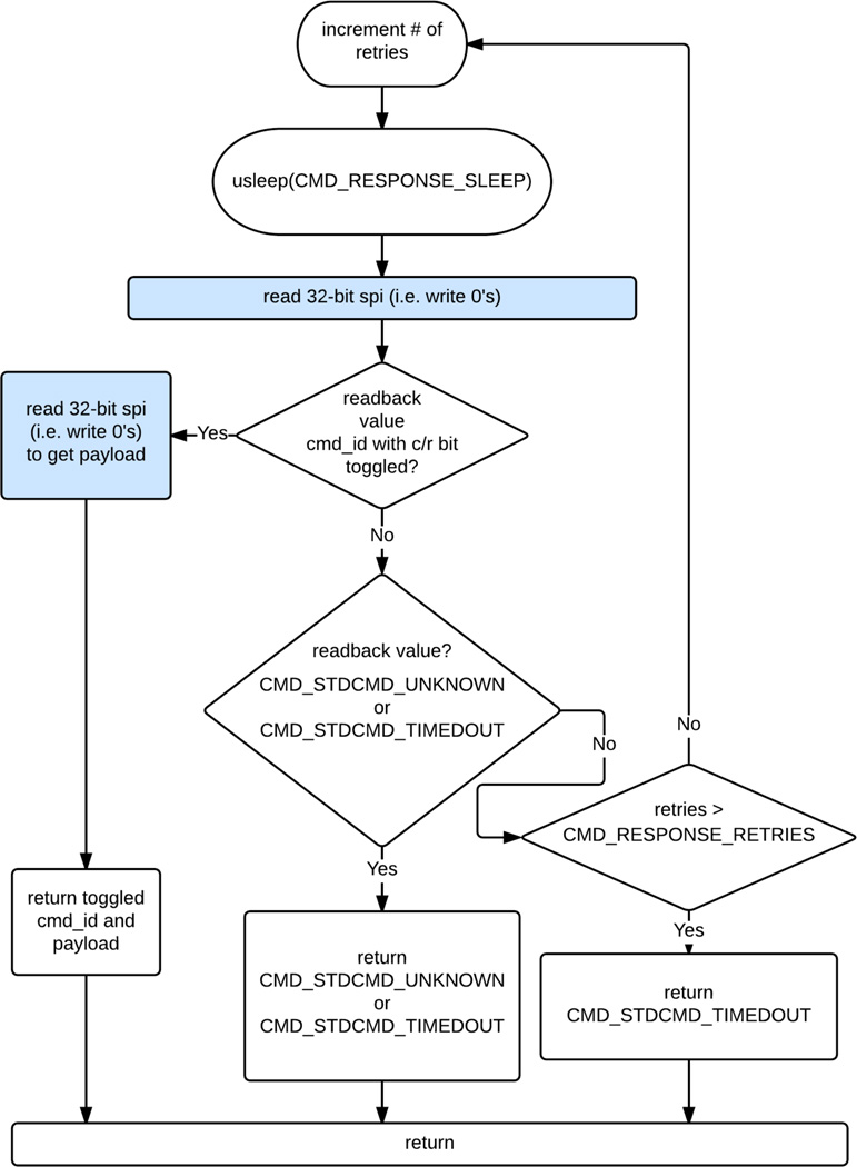
SPI does not allow slaves (i.e., children) to initiate a transaction by design. Consequently, the master (i.e., parent) has to perform a read SPI transaction by writing 0’s to a destined slave. The flow of SPI commands is shown in Fig. 11 where blocks labeled “spi write” and “spi read” represent C functions in the embedded software. These functions are depicted in Fig. 13 and Fig. 12 respectively.
Fig. 11.
SPI software processing flow. Once a command is received, via QuickUSB or Ethernet, it goes through this flow in order to generate a proper reply to the source.
Fig. 13.
OpenPET SPI write() C function. A non-zero return value is considered an error.
Fig. 12.
OpenPET SPI read() C function. The returned value of this function is passed through to the source. CMD_* are predefine constants in the embedded software. The constants names used in this figure are descriptive.
SPI slaves differentiate between a write SPI transaction and a read transaction by looking at the SPI data. If it is all zeros, it is considered a SPI read. To implement this in an efficient way, OpenPET utilizes NIOS interrupts, such that any SPI transaction on a slave will cause the NIOS microprocessor on that slave to wake up and execute an Interrupt Service Routine (ISR). If an SPI transaction does not finish within a specified timeout period, it will be dropped and ignored. Also, if a slave is flooded with SPI reads or writes before it finishes, the slave will always provide the last valid reply saved on its output port; thus, alerting the master that it is busy.
C. Generic embedded software and firmware interface
Once an SPI command reaches a node, if this command is to be executed within the node’s firmware, then it has to be directed to a specific firmware module for proper execution. Accordingly, Altera’s Parallel IO (PIO) soft cores are used to create a generic interface between the NIOS software and the FPGA fabric. Each command received will be sent to the firmware on a 16-bit wide bus along with a 1-bit valid signal. The firmware registers incoming commands on the rising edge of the valid signal and returns a reply to NIOS on another 16- bit bus in order to allow duplex operations. An additional 1-bit valid signal is used to notify the NIOS that a reply is ready. This valid bit is used as an interrupt to trigger an ISR function which handles Software-Firmware Interface commands. Once a valid reply is acquired in software, it will be saved in the SPI output port buffer. Therefore, the next time the SPI master (i.e. parent) performs a read operation, the reply will be readily available.
IV. Workstation Computer Software
The OpenPET platform provides multiple software packages. A detailed description of these packages is beyond the scope of this manuscript; thus, we provide a short summary of what is available. First, two command line executables are available to issue command and acquire data. An OpenPET system can be configured and run with just these two executables. Second, a data acquisition and analysis software for running an OpenPET system called OpenPET Control and Analysis Tools (CAT) has been implemented using the ROOT framework [7]. OpenPET CAT can be executed using a graphical user interface (GUI) or command line scripts. Third, a Python script, has been implemented to serve as an automated test script for new firmware and software builds, and to validate the configuration of the OpenPET system.
V. Open Source Management
An open source software, firmware, and hardware project requires a lot of resources to manage and track its development and growth. The amount of time and effort required to provide the following components and services is not negligible or trivial, and they are considered as the foundation that the OpenPET platform floats on and sails with:
A. Website
The OpenPET website is hosted internally at Lawrence Berkeley National Laboratory servers. The website is served off of a Virtual Machine to allow easier migration, recovery, and maintenance. The content management system used is Wordpress, which allows us to quickly update, publish, and maintain the website for the OpenPET community.
Communication among users and developers is crucial for any open source project; therefore, we provide multiple forums (hosted on our website) for discussions and support. Additionally, a mailing list is used to distribute emails across users and developers quickly.
B. Repository
OpenPET uses BitBucket [8], a distributed revision control system site for Git and Mercurial in the cloud. Each component of the OpenPET platform is revision controlled and tracked. For software development like C++ and Python, using revision control is standard and simple. However, for hardware components like PCB design files and firmware development, using revision control is not trivial. As a result, multiple repositories are created for each hardware component. For example, the Support Board has its own repositories with multiple subdirectories, where each subdirectories contains (i) hardware design files like Cadence Orcad or Allegro. (ii) Firmware design files like Altera’s Quratus II project, HDL components, and Qsys project. (iii) Software files like Eclipse project, C embedded software running on NIOS, Board Support Package (BSP) generation scripts, etc. (iv) Scripts which are cross-platform (Windows batch scripts and GNU/Linux shell scripts) files that facilitate many complex, iterative, and time consuming functions: (a) generation of an integrated bitstream image for the Support Board, that is, compile and build 3 different Quartus projects for 3 FPGAs, 3 Qsys projects, 3 Eclipse project, merge the firmware (SRAM Object File -- SOF) with its corresponding embedded software (Executable and Linkable Format -- ELF) and combine all 3 imaged into a single “flashable” image to be stored on EPCS; (b) generation of an integrated image to the Detector Board. The process is similar to Support Board but doesn’t require 3 FPGAs; (c) simplified flashing and programming, where a user executes simple scripts to program the entire system; and (d) automated build and test flows where the software and firmware repositories of the entire system can be periodically tested on actual hardware.
The hardware design files and the source code for the firmware, software, and scripts can be found in our public repository [8].
VI. Results
OpenPET platform results are presented as overall system performance as well as functional verifiability.
A. System Performance
A full configuration of the entire system followed by raw data acquisition using the Scope mode serves as an excellent measure of performance. The system is configured with the data bus is running at 80 MHz, i.e., default OpenPET system frequency, the data mode is set to Scope mode, all channel trigger masks are enabled, and a low DAC threshold for triggers is set. These settings will saturate the data path all the way to the uppermost node where the QuickUSB module is connected. A dual clock FIFO manages the output data stream between the OpenPET chassis, the QuickUSB module, and the workstation. The incoming data rate of that FIFO is 1280 Mbps (i.e. 80 MHz * 16-bits), and the outgoing rate is 480 Mbps.
After running the Scope mode for few minutes, we have measured the throughput at the workstation to be around 320 Mbps. This is less than 480 Mbps because USB 2.0 never reaches its maximum theoretical speed due to software and CPU/memory limitations on the workstation.
B. Functionality
The same test setup used to acquire System Performance results is also used to verify the functionality of the platform. However, the main difference is that the ADC is configured to output fixed-pattern data samples which are eventually transferred to the uppermost node, the QuickUSB module, and then to the workstation computer storage. The recorded data is validated for integrity by verifying that the data on disk equals the predefined fixed-pattern data generated by the ADC.
We validated data integrity and platform functionality by collecting and storing 2GB of fixed-pattern ADC on disk, and verifying that the stored data and headers were equal to the expected values.
C. Experiment
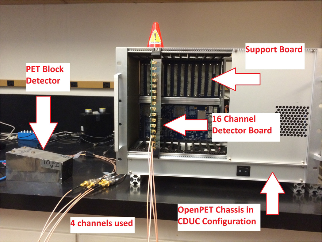
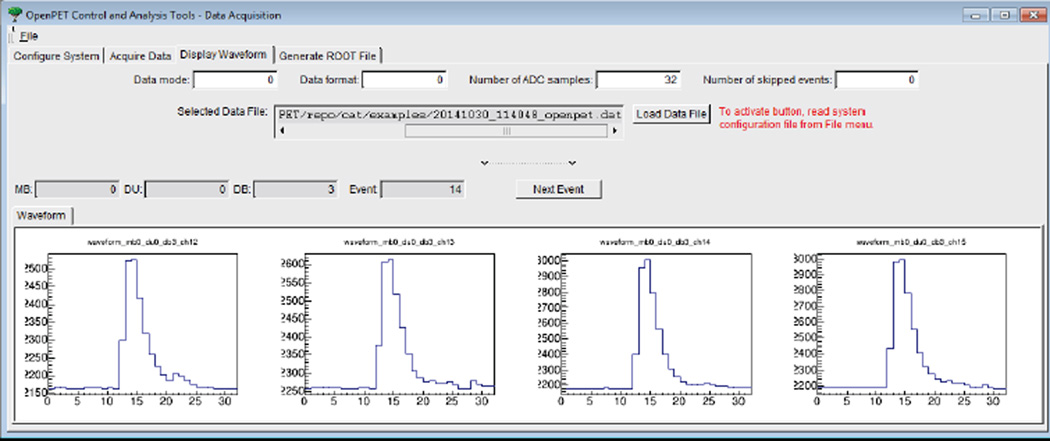
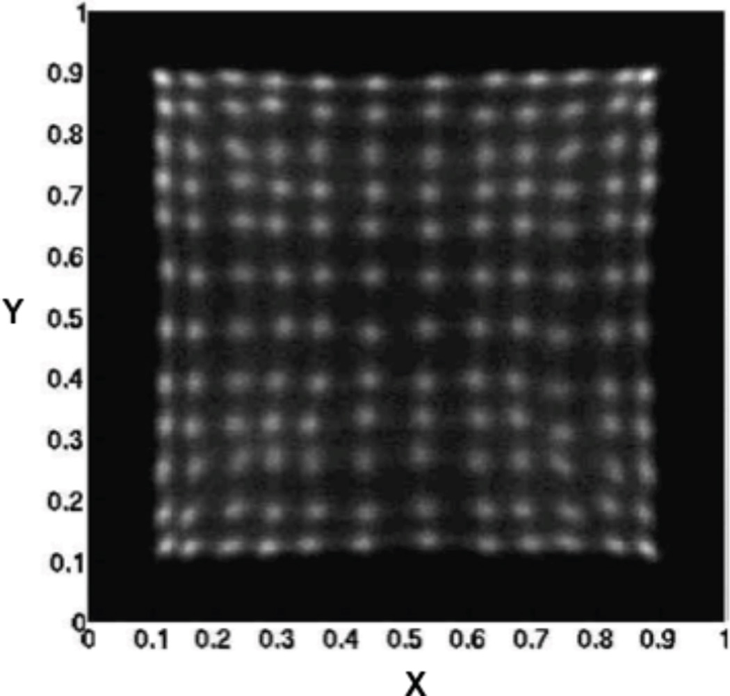
A prototype PET block detector, which consists of a 12×12 array of 4×4 22mm3 LSO crystals read out with four Hamamatsu R-9800 Photo Multiplier Tubes (PMT), was setup as photographed in Fig. 14. Each PMT output was sent to an input channel of the OpenPET 16-channel Detector Board [2]. The total amount of energy observed by each of the four PMTs (A, B, C, and D) was determined by integrating the analog signals. These four energies were then summed to estimate the total energy (E=A+B+C+D) of the event. The appropriate Anger logic (X=(A+B)/E and Y=(B+D)/E) was computed to give an estimate of the position of interaction for the event. Fig. 15 shows the acquired digitized data stored on disk using OpenCAT GUI and Fig. 16 shows the flood map for events with energy greater than 350 keV. The average energy resolutions from all the 144 crystals were found to be around 12% fwhm.
Fig. 14.
Experimental setup for a PET block Detector and OpenPET platform.
Fig. 15.
OpenCAT GUI software showing the acquired digitized signals from the conventional PET block detector module.
Fig. 16.
Flood map for the data collected from the experiment.
Further experiments are performed in [2] which exceed the expected performance metrics stated in Section I.B. We reported a 0.3% energy resolution (compared with <2%) of an HPGe detector when excited with 662 keV gamma rays and 90 ps fwhm timing resolution (compared with <100 ps) by splitting a test pulse to two channels and measuring the difference.
VII. Conclusion
The OpenPET platform provides a solid open source hardware, firmware, and software packages for multi-channel data acquisition and analysis. The flexibility and modularity of the hardware, firmware, and software makes it very appealing to a wide range of applications, i.e., nuclear imaging, detection, and non-proliferation applications. We have described the architecture and implementation of the firmware as well as the embedded software and provided experimental results to show the suppleness and performance of the platform.
Acknowledgments
This work was supported in part by the Director, Office of Science, Office of Biological and Environmental Research, Medical Science Division of the U.S. Department of Energy under Contract DE-AC02-05CH11231, and in part by the National Institutes of Health, National Institute of Biomedical Imaging and Bioengineering under Grants R01EB016104
References
- 1.Moses WW, Buckley S, Vu C, Peng Q, Pavlov N, Choong W-S, Wu J, Jackson C. OpenPET: A Flexible Electronics System for Radiotracer Imaging. IEEE Transactions on Nuclear Science. 2010 Oct.57(5):2532–2537. doi: 10.1109/NSSMIC.2009.5401797. [DOI] [PMC free article] [PubMed] [Google Scholar]
- 2.Choong W-S, Abu-Nimeh F, Moses WW, Peng Q, Vu CQ, Wu J-Y. A front-end readout Detector Board for the OpenPET electronics system. Journal of Instrumentation. 2015 Aug.10(08):T08002–T08002. doi: 10.1088/1748-0221/10/08/T08002. [DOI] [PMC free article] [PubMed] [Google Scholar]
- 3.OpenPET official website. [Accessed: 08-Jul-2015]; [Online]. Available: https://openpet.lbl.gov/
- 4.Wu J, Shi Z. The 10-ps wave union TDC: Improving FPGA TDC resolution beyond its cell delay; IEEE Nuclear Science Symposium Conference Record, 2008. NSS ’08; 2008. pp. 3440–3446. [Google Scholar]
- 5.QuickUSB Module. [Accessed: 20-Jul-2015]; [Online]. Available: http://www.bitwisesys.com/qusb2-p/qusb2.htm. [Google Scholar]
- 6.Nios II UDP Offload Example - Altera Wiki. [Accessed: 20-Jul-2015]; [Online]. Available: http://www.alterawiki.com/wiki/Nios_II_UDP_Offload_Example. [Google Scholar]
- 7.ROOT | A Data Analysis Framework. [Accessed: 20-Jul-2015]; [Online]. Available: https://root.cern.ch/drupal/ [Google Scholar]
- 8.OpenPET — Bitbucket. [Accessed: 06-Jul-2015];OpenPET Repository. [Online]. Available: https://bitbucket.org/openpet/ [Google Scholar]


