Abstract
We present a 16-channel front-end readout board for the OpenPET electronics system. A major task in developing a nuclear medical imaging system, such as a positron emission computed tomograph (PET) or a single-photon emission computed tomograph (SPECT), is the electronics system. While there are a wide variety of detector and camera design concepts, the relatively simple nature of the acquired data allows for a common set of electronics requirements that can be met by a flexible, scalable, and high-performance OpenPET electronics system. The analog signals from the different types of detectors used in medical imaging share similar characteristics, which allows for a common analog signal processing. The OpenPET electronics processes the analog signals with Detector Boards. Here we report on the development of a 16-channel Detector Board. Each signal is digitized by a continuously sampled analog-to-digital converter (ADC), which is processed by a field programmable gate array (FPGA) to extract pulse height information. A leading edge discriminator creates a timing edge that is “time stamped” by a time-to-digital converter (TDC) implemented inside the FPGA. This digital information from each channel is sent to an FPGA that services 16 analog channels, and then information from multiple channels is processed by this FPGA to perform logic for crystal lookup, DOI calculation, calibration, etc.
Keywords: Time-of-flight, Positron emission computed tomography, Field programmable gate array, Analog-to-digital converter, Time-to-digital converter
1. Introduction
The purpose of the OpenPET electronics [1–2] is to provide electronics for a large variety of users, primarily researchers who are developing prototype nuclear-medical imaging systems. These electronics must be extremely flexible, as the type of detector will vary from system to system.
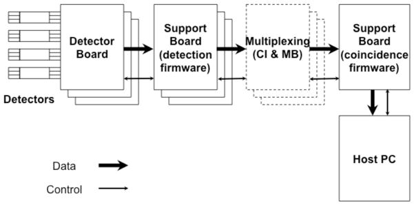
The OpenPET system architecture is shown in Fig. 1. There are four types of custom electronics boards in the system: the Detector Board (DB), Support Board (SB), Coincidence Interface Board (CI), and Multiplexer Board (MB). The SB plays two roles in the system, depending on its firmware.
Figure 1.
Schematic diagram of the OpenPET system architecture.
The general data flow is that analog signals from detector modules provide the inputs to the DB. This DB processes the analog signals to create a singles event word, which is a digital representation of a single gamma ray interaction in the detector module. These singles event words are passed to the SB loaded with detection firmware, whose main function is to multiplex the singles event words from multiple DBs. The singles event words are then passed through the CI to the MB, which can provide a further layer of multiplexing for singles event words, if necessary. Next the multiplexed singles event words are passed to another SB loaded with coincidence firmware, which searches through the singles event words for pairs that are in time coincidence and then forms coincidence event words. These coincidence event words are then passed to the host PC.
The OpenPET electronics must have high performance to service state-of-the-art systems. The important performance characteristics are: a large number of channels (>1000), high maximum count rate (>106 singles events/second and coincidence events/second), good energy resolution (<2% fwhm for test pulses), and good timing resolution (<1ns fwhm for conventional PET, <100 ps fwhm for time-of-flight PET). Low cost and low power consumption are also important properties.
Over the past decade, the radiation detectors proposed include different scintillators (NaI:Tl, CsI:Tl, BGO, LSO, GSO, YAP, LuAP, etc.) coupled to a wide variety of photodetectors, such as photomultiplier tubes (PMTs), multi-anode PMTs, position-sensitive PMTs, PIN photodiodes, avalanche photodiodes (APDs), position-sensitive APDs, hybrid photodetectors, vacuum avalanche photodetectors, silicon photomultipliers (SiPMs), as well as solid-state detectors such as silicon, high-purity germanium (HPGe), and cadmium zinc telluride (CZT). The signals from the detectors can be combined in a wide variety of ways, ranging from simple (e.g., individual coupling and four channel “block detectors”) to moderately complex (e.g., Anger cameras that read out dozens of PMTs and row/column readout) to highly complex (e.g., position-sensitive detectors on both ends of a scintillator crystal array and schemes that use an array of photosensors to infer the three-dimensional position of interaction within a crystal). Finally, there are many variations in camera geometry, such as single ring, parallel plane, six-sided box, octagonal, insert plus ring, and Compton scatterer plus secondary interaction ring.
While there are a tremendous number of variations, the analog signals from most detectors are very similar—a pulse whose area is proportional to the deposited energy and whose leading edge is used to extract a timing signal. This allows a general design of the DB to service many different types of detectors. In this paper, we report on the development and performance of a 16-channel DB for the OpenPET electronics.
2. Detector Board
2.1 General board design
The overall purpose of the DB is to process the analog inputs from the detector modules in the system and convert them into singles event words. Generally, this requires determining the energy, interaction position, and arrival time associated with a single gamma ray interaction in the detector module, and as many corrections as possible should be applied before the singles event word is generated.
The DB generally consists of an analog front-end circuit to process the analog input signal, which involves amplification and filtering to reduce the noise and bandwidth of the signal. The processed analog signal is subsequently digitized with an analog-to-digital converter (ADC) to capture the processed analog signal. For systems that require good timing resolution such as PET, additional circuitry may be implemented in the front-end to split the analog input signal to provide a fast timing path where the signal is amplified with a high-bandwidth amplifier. The amplified signal is subsequently triggered by a fast leading edge discriminator to create a timing pulse for the arrival of the signal that is time stamped by a time-to-digital converter (TDC) implemented inside the FPGA [3].
The back-end of the DB primarily consists of an FPGA and static random access memory (SRAM). The FPGA processes the digitized signals from the ADCs and, if necessary, combines information from multiple channels to compute the deposited energy, the interaction position, and the event time. Appropriate calibration correction factors that are stored in the SRAM can also be applied to the data. The computed information are formatted into a singles event word and then transferred to the SB via the standard OpenPET Bus IO. In addition, the firmware for the FPGA is loaded into the DB by the SB via the standard Bus IO between the SB and DB as described in next subsection. Note that different firmware can be loaded into the FPGA to perform tasks other than event processing, such as debugging, testing, and calibration.
2.2 Bus IO
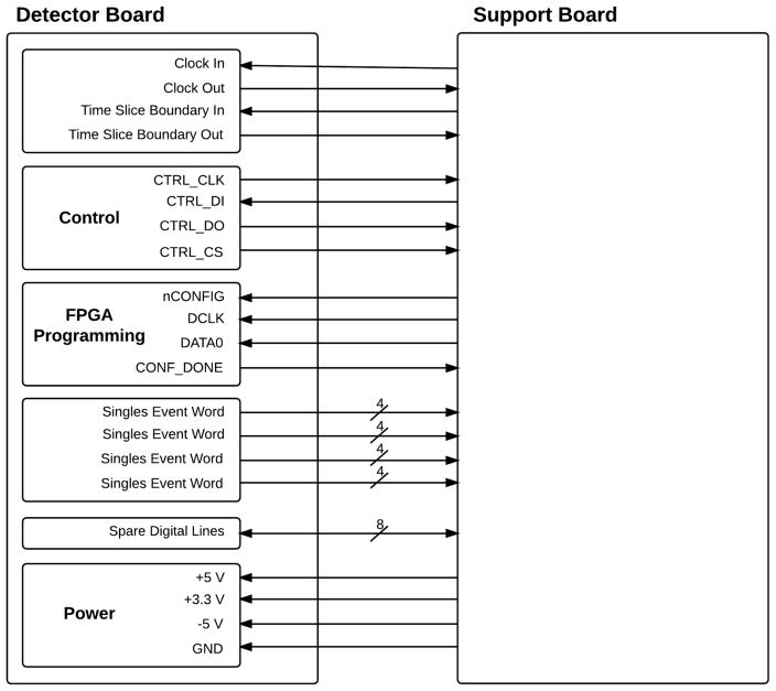
The Bus IO connecting the DB to the SB is shown schematically in Fig. 2. The bus is divided into several blocks. One block provides the timing signals using 4 LVDS differential pairs. There are two fundamental timing signals in the OpenPET system – an 80 MHz System Clock signal generated on the SB and a Time Slice Boundary signal that defines the beginning of a Time Slice. The SB sends a copy of these System Clock and Time Slice Boundary signals, which are used to clock data from the SB to the DB. Because there is propagation delay within the DB, another copy of the System Clock and Time Slice Boundary signals (that is produced by the DB) is used to clock data from the DB to the SB. In the OpenPET architecture, the system divides time into small, fixed time slices of either 100 ns (8 clocks) or 200 ns (16 clocks). Alternatively, custom time slices can be designed by modification of the firmware, if needed.
Figure 2.
Schematic diagram of the Bus IO between the DB and SB.
A second block defines 4 LVTTL single-ended lines to control data between the DB and SB. These control lines can be configured to support standard digital serial protocols such as I2C or SPI or a customized digital serial communication.
A third block provides 4 LVTTL single-ended lines to program the FPGA on the DB using serial protocols, which are generated by the SB.
A fourth block provides 16 LVDS differential pairs (grouped into 4 sets of 4 LVDS differential pairs) to transfer singles event words from the DB to SB. All individual operations must occur within a single time slice, which implies that only single event words that occur in the same time slice can be combined to form a coincident event. A single event word can be either a 32-bit word (100 ns time slice) or 64-bit word (200 ns time slice). Since it can take significantly longer than a single time slice to fully process a single event, the system is pipelined so that the processing is divided into smaller steps that can each be completed in a single time slice. During one time slice, each set of 4 LVDS differential pairs can pass one singles event word (i.e. maximum of 4 singles event words per time slice). Thus, the maximum singles event rate that can be transferred out of each DB is 40 million events per second.
Another block provides 8 spare LVDS differential pairs between the DB and SB for users to pass any information between these two boards.
The final block supplies power to the DB: +5V, +3.3V −5V, and ground.
2.3 16-channel Detector Board
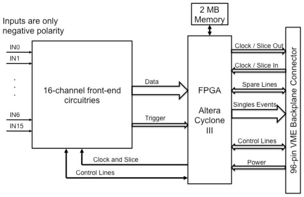
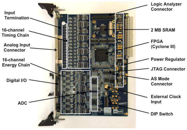
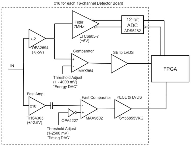
Fig. 3 shows the block diagram of the 16-channel DB. Fig. 4 shows a photograph of the 16-channel DB. This DB accepts up to 16 analog input signals, each of which is processed independently. The analog input signal is required to be negative polarity, ground referenced. The input analog signal is terminated with 50 ohm, and then split into two processing chains: an energy chain and a timing chain. The processing circuit for one channel is shown in Fig. 5. The input stage accepts voltages between −0.8 V to 0 V. The input voltage can be attenuated to fall within the acceptable range by changing the attenuation resistor values on the energy chain. Only the signal on the energy chain needs to be attenuated, because the range of the input voltage is limited by the dynamic range of the ADC. In addition, there are 8 external differential LVDS IO pairs that can be used to interface to the DB FPGA. The flexibility of these digital IO will allow any digital inputs and/or outputs to be applied to the DB.
Figure 3.
Block diagram of the 16-channel DB.
Figure 4.
Photograph of the 16-channel DB.
Figure 5.
Block diagram of the front-end circuitries of one channel of the 16-channel DB.
On the energy chain, the input signal is amplified (OPA2694), and then split into an anti-aliasing filter (LTC6605-7) with a cut-off frequency at 7 MHz and a comparator (MAX964). The filtered signal is sent to a 12-bit ADC (ADS5282) that can digitize the signal at a sampling rate from 10 MSPS to 65 MSPS. Each channel of the ADC also has a programmable digital gain from 0 dB to 12 dB. A trigger is generated by the comparator and sent to the FPGA.
On the timing chain, the input signal is amplified with an ×10 high-bandwidth (1.8 GHz) amplifier and then sent to a fast comparator (MAX9602) with low propagation delay dispersion (~30 ps) to trigger on the leading edge of the analog signal. We have selected a leading edge discriminator, since several groups have reported that a leading edge discriminator has equivalent or better performance than a constant fraction discriminator (although sometimes requiring amplitude correction for time walk) [4]–[8]. The generated timing pulse from the comparator is then sent to the FPGA, where a TDC is implemented to determine the time stamp of the arrival time of the timing signal.
Table 1.1 summarizes the specifications of the 16-channel DB.
Table 1.1.
Specifications of the 16-channel Detector Board
| General | |
| Form factor | 6U VME |
| Input power supply | +3.3V, +5V, −5V |
| Analog Input | |
| Number of channels | 16 |
| Input voltage range | −0.8 to 0 V |
| Input impedance | 50 ohm single-ended |
| Input bandwidth | 1.8 GHz |
| Anti-aliasing filter bandwidth | 7 MHz |
| Analog-to-Digital Conversion | |
| Sampling speed | 10 to 65 MSPS |
| Resolution | 12 bits |
| Energy resolution | < 2 keV |
| Timing Characteristics | |
| High-resolution FPGA-based TDC | < 30 ps LSB |
| Timing resolution | < 100 ps fwhm |
| Front Panel Digital I/O | |
| Number of inputs | 4 LVDS pairs |
| Number of outputs | 4 LVDS pairs |
| Memory | |
| SRAM | 2 MB |
| FLASH | 8 MB |
| Backplane Digital Bus I/O | |
| Maximum clock speed | 80 MHz |
| Number of slow communication lines | 4 LVTTL |
| Number of data output lines | 16 LVDS pairs |
3. Performance measurement
We have fabricated and tested production versions of the 16-channel DB and SB. A Detector Unit is constructed with one 16-channel DB plugged into it. The SB is interfaced to the host PC through a USB 2.0 link on the SB for control communication and data transfer.
3.1 Energy resolution of scintillation detectors
Two scintillation detectors were used to evaluate the performance of the 16-channel DB. These scintillation detectors were prototype PET detectors consisting of either a 6.15 × 6.15 × 25 mm3 LSO crystal or a 6.15 × 6.15 × 25 mm3 LaBr3 crystal, which was coupled to a Hamamatsu R-9800 PMT on one of their 6.15 × 25 mm2 faces. The R-9800 PMT had a super-bialkali photocathode.
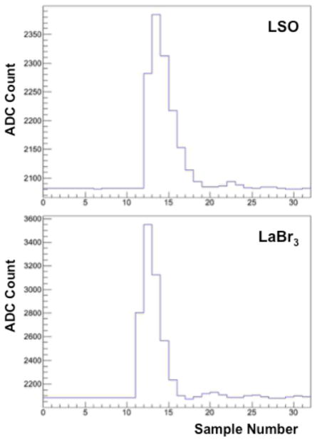
The detectors were excited with 511 keV gamma rays from a positron source (Ge-68). The analog signal from the PMT was sent to one input channel of the DB. The digitized signals from the ADC sampling at a rate of 40 MSPS were transferred from the DB to the SB and then subsequently to the host PC event-by-event. A sample of the digitized signals from both detectors are shown in Fig. 6. Note that the decay time of the LSO signal was slightly longer than that of the LaBr3 signal, which was indicative of the slightly longer scintillation decay time of LSO compared to LaBr3. The energy of each event was determined by integrating the analog signal (i.e., area under the curve). Fig.s 7 and 8 show the energy spectra for the detectors with LSO and LaBr3 crystals respectively. The LSO detector had an energy resolution of 15.5% fwhm, whereas the LaBr3 detector had an energy resolution of 6.1% fwhm. As a comparison, we determined the energy of both detectors using high-performance NIM electronics and obtained energy resolutions of 14.4% fwhm and 4.7% fwhm for the LSO and LaBr3 detectors respectively.
Figure 6.
Sample of the digitized detector signals from the LSO (top) detector and LaBr3 (bottom) detector.
Figure 7.
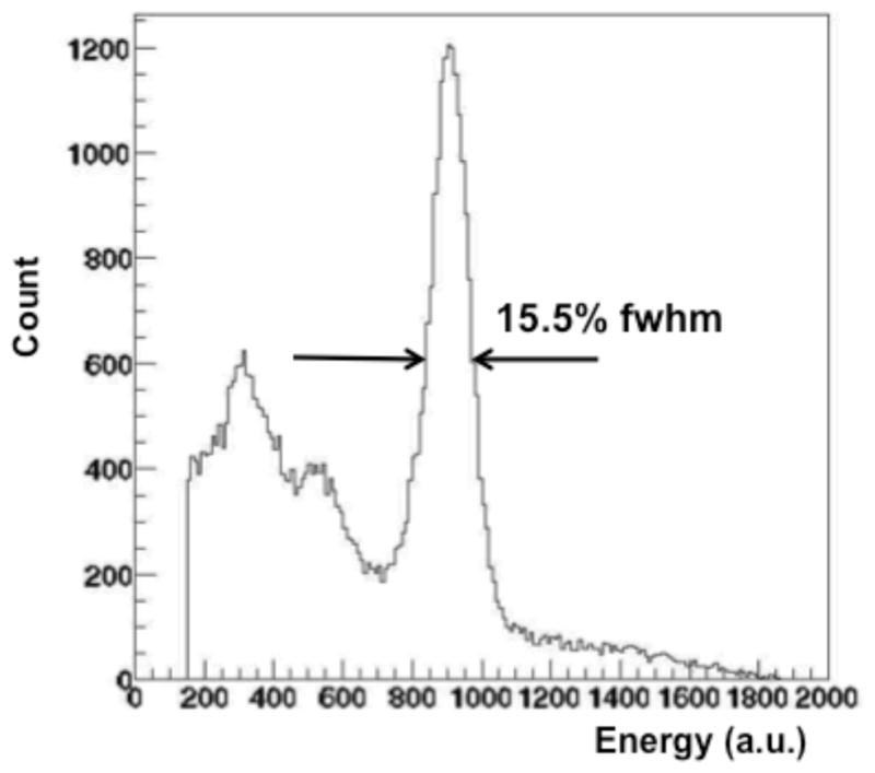
Energy spectrum of the LSO detector when excited with 511 keV gamma rays.
Figure 8.
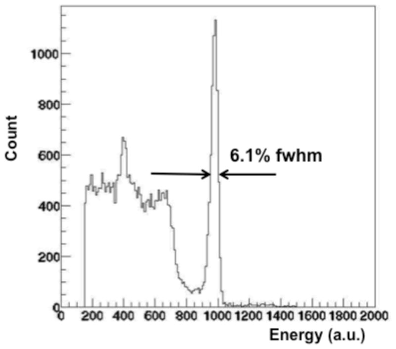
Energy spectrum of the LaBr3 detector when excited with 511 keV gamma rays.
3.2 Energy resolution of an HPGe detector
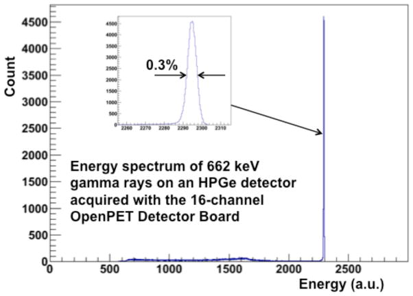
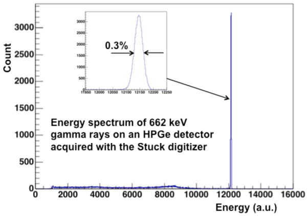
In addition to the scintillation detectors, a standard planar HPGe detector was used to evaluate the spectroscopic performance of the 16-channel DB. The detector was excited with 662 keV gamma rays from a Cs-137 source. The analog signal from the detector was read out with a preamplifier. The fall time of the preamplifier is about 50 μs to ensure complete charge collection. The output of the preamplifier was sent to one input of the 16-channel DB. The digitized signals from the ADC sampling at a rate of 40 MSPS were transferred from the DB to the SB and then subsequently to the host PC event-by-event. The energy of each event is calculated by applying a trapezoidal filter [9] to the digitized pulses. Fig. 9 shows the energy spectrum for the HPGe detector measured with the 16-channel DB and an energy resolution of 0.3% fwhm was obtained. We also compared the spectroscopic performance of the 16-channel DB with a commercial 8-channel 200 MHz 12-bit digitizer (Model SIS3320) from Struck Innovative System. We repeated our measurement sampling the preamplifier outputs at 100 MSPS with the Struck digitizer and applying the same trapezoidal filter to the digitized pulses. Fig. 10 shows the energy spectrum for HPGe detector measured with the Struck digitizer and an energy resolution of 0.3% fwhm was obtained.
Figure 9.
Energy spectrum of an HPGe detector when excited with 662 keV gamma rays, and acquired with the 16-channel DB.
Figure 10.
Energy spectrum of an HPGe detector when excited with 662 keV gamma rays, and acquired with the Struck digitizer.
3.3 Readout of a PET block detector module
The 16-channel DB performance was also evaluated using a conventional PET block detector module. This was a prototype block detector module consisting of a 12 × 12 array of 4 × 4 × 22 mm3 LSO crystals read out with four Hamamatsu R-9800 PMTs operated at -1300 V. The detector module was excited with 511 keV gamma rays from a positron source (Ge-68). Each PMT output was sent to an input channel of the 16-channel DB. An event trigger was generated whenever any one of the four channels triggered. The digitized signals from the ADC sampling at a rate of 40 MSPS were transferred from the DB to the SB and then subsequently to the host PC event-by-event. The total amount of energy observed by each of the four PMTs (A, B, C, and D) was determined by integrating the analog signals. These four energies were then summed to estimate the total energy (E=A+B+C+D) of the event. The appropriate Anger logic (X=(A+B)/E and Y=(B+D)/E) was computed to give an estimate of the position of interaction for the event. Fig. 11 shows the flood map for events with energy greater than 350 keV. Each of the 144 crystals is clearly distinguished. The average energy resolution from all the 144 crystals was found to be about 12% fwhm.
Figure 11.
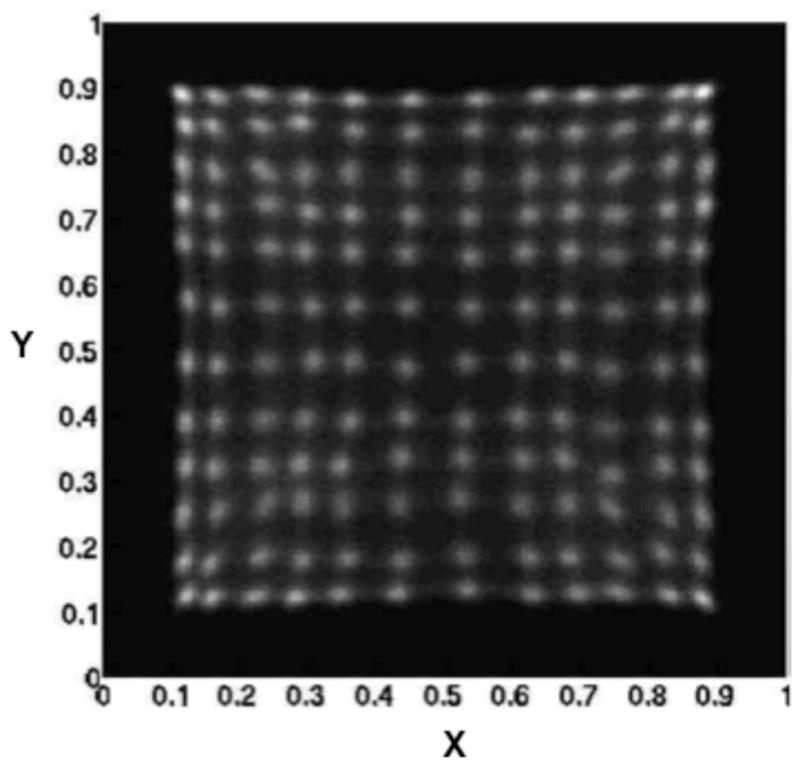
Flood map form a PET block detector module.
3.4 TDC
A 16-channel firmware TDC was implemented in the Altera Cyclone III FGPA on the 16-channel DB. The TDC was implemented using the Wave Union approach, as described in [10–11]. The performance was tested with a digital test pulse that was split into two different input channels of the 16-channel DB. The timing pulse from the timing chain was used to trigger the TDC. The time stamp generated by the TDC from the two channels were transferred from the DB to the SB and then subsequently to the host PC event-by-event. The histogram of time difference between the two channels is plotted in Fig. 12. The timing resolution of the TDC was about 90 ps fwhm, which represents the intrinsic timing resolution of the implemented TDC on the 16-channel DB. While the timing accuracy of the implemented TDC can be improved, its performance on the 16-channel DB sufficient even for high-performance time-of-flight systems.
Figure 12.
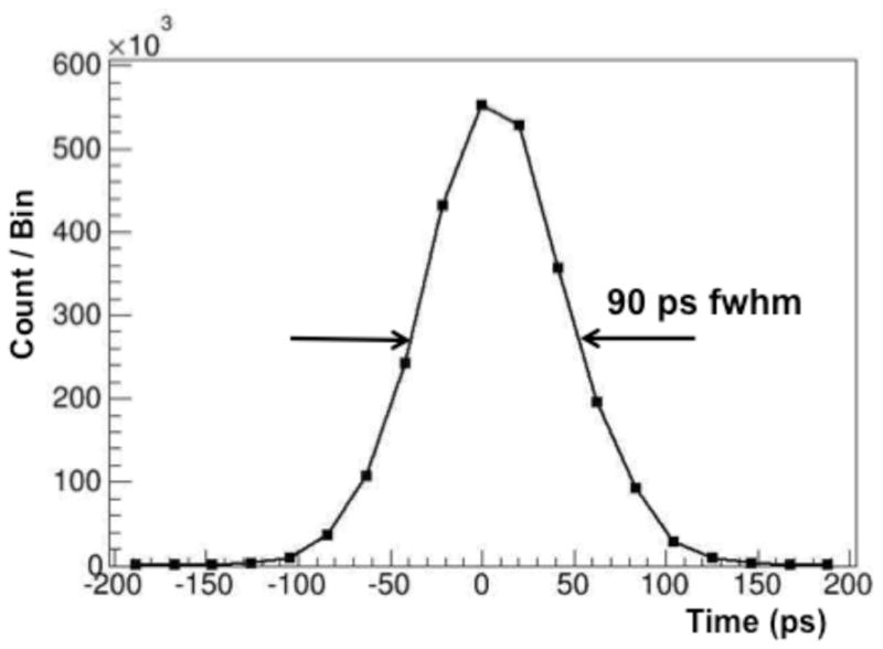
Time difference spectrum obtained with a digital test pulse split into two input channels of the 16-channel DB.
4. Discussion and conclusions
We have developed a 16-channel Detector Board for the OpenPET electronics system. This DB serves as the front-end readout board, processing detector analog signals from nuclear-medical imaging systems. Each channel processes the analog signal with an energy chain and a timing chain. The filtered analog signal is digitized with an ADC, which increases the flexibility and performance when processing the digitized signal to determine the relevant information specific to the detector system (i.e., energy, interaction position, etc.). The timing measurement utilizes a leading edge discriminator and FPGA-based TDC to generate an accurate timing signal to determine the arrival time of the signal.
Measurements with prototype scintillation detectors with LSO and LaBr3 crystals demonstrated an energy resolution of 15.5% fwhm and 6.1% fwhm respectively when excited with 511 keV gamma rays. The same measurement performed with high-performance NIM electronics gave energy resolutions of 14.4% fwhm and 4.7% fwhm respectively. The measurements with the 16-channel DB used a simple integration of the digitized signal to determine the energy of the signal. While the energy resolution measured with the 16-channel DB using a simple of integration is slightly worse than that measured with the high-performance NIM electronics, its performance meets our requirements for nuclear medical imaging applications.
While the design of the front-end of the 16-channel DB is not optimized for high signal-to-noise ratio, the spectroscopic performance of the 16-channel DB proves to be very good when the maximum frequency of the analog signal is low enough to be completely determined by the sampling rate of the ADC (Nyquist-Shannon sampling theorem) and the appropriate digital signal filter is applied to the digitized signal. Comparison with an optimized digitizer from Struck gave similar energy resolution of 0.3% for an HPGe detector when excited with 662 keV gamma rays.
Readout of a PET block detector module using LSO crystals with the 16-channel DB clearly distinguished all the crystals (4 PMTs decoding 144 crystals with Anger logic) in the block detector. The average energy resolution from all the 144 crystals was about 12% fwhm. This further supports that the 16-channel DB meets the performance requirements for the many different types of detector used in nuclear-medical imaging systems.
A TDC is implemented in the 16-channel DB FPGA using the Wave Union approach. Measurements with test pulses gave a timing resolution of 90 ps fwhm. While this timing resolution meets the requirement for high-performance time-of-flight systems, the performance of the TDC can be improved with further firmware optimization and/or by averaging over multiple measurements [11].
Acknowledgments
This work was supported in part by the Director, Office of Science, Office of Biological and Environmental Research, Medical Science Division, U.S. Department of Energy under contract DE-AC02-05CH11231, and in part by the National Institutes of Health, National Institute of Biomedical Imaging and Bioengineering, under Grant Number R01EB016104.
References
- 1.Moses WW, et al. OpenPET: A flexible electronics system for radiotracer imaging. IEEE Trans Nucl Sci. 2010;57:2532. doi: 10.1109/NSSMIC.2009.5401797. [DOI] [PMC free article] [PubMed] [Google Scholar]
- 2.http://openpet.lbl.gov.
- 3.Wu J. Firmware-only implementation of time-to-digital converter (TDC) in field-programmable gate array (FPGA) IEEE Nucl Sci Symp Conf Rec. 2003:177. [Google Scholar]
- 4.Szczesniak T, et al. A further study of timing with LSO on XP20D0 for TOF PET. IEEE Trans Nucl Sci. 2007;54:1464. [Google Scholar]
- 5.Haselman MD, et al. Simulation of algorithms for pulse timing in FPGAs. IEEE Nucl Sci Symp Conf Rec. 2007:3161. doi: 10.1109/NSSMIC.2007.4436798. [DOI] [PMC free article] [PubMed] [Google Scholar]
- 6.Genat JF, et al. Signal processing for picosecond resolution timing measurements. Nucl Instr Meth A. 2009;607:387. [Google Scholar]
- 7.Choong WS. The timing resolution of scintillation-detector systems: Monte Carlo analysis. Phys Med Biol. 2009;54:6495. doi: 10.1088/0031-9155/54/21/004. [DOI] [PMC free article] [PubMed] [Google Scholar]
- 8.Ambrosi G, et al. Time resolving characteristics of HPK and FBK silicon photomultipliers for TOF and PET applications. Nucl Instr Meth A. 2010;617:242. [Google Scholar]
- 9.Jordanov V, Knoll G. Digital synthesis of pulse shapes in real time for high resolution radiation spectroscopy. Nucl Instr Meth A. 1994;345:337. [Google Scholar]
- 10.Wu J, Shi Z. The 10-ps wave union TDC: improving FPGA TDC resolution beyond its cell delay. IEEE Nucl Sci Symp Conf Rec. 2008:3440. [Google Scholar]
- 11.Wu J. An FPGA TDC for time-of-flight applications. IEEE Nucl Sci Symp Conf Rec. 2009:299. [Google Scholar]


