Abstract
Silicon compatible wafer scale MoS2 heterojunctions are reported for the first time using colloidal quantum dots. Size dependent direct band gap emission of MoS2 dots are presented at room temperature. The temporal stability and decay dynamics of excited charge carriers in MoS2 quantum dots have been studied using time correlated single photon counting spectroscopy technique. Fabricated n-MoS2/p-Si 0D/3D heterojunctions exhibiting excellent rectification behavior have been studied for light emission in the forward bias and photodetection in the reverse bias. The electroluminescences with white light emission spectra in the range of 450–800 nm are found to be stable in the temperature range of 10–350 K. Size dependent spectral responsivity and detectivity of the heterojunction devices have been studied. The peak responsivity and detectivity of the fabricated heterojunction detector are estimated to be ~0.85 A/W and ~8 × 10¹¹ Jones, respectively at an applied bias of −2 V for MoS2 QDs of 2 nm mean diameter. The above values are found to be superior to the reported results on large area photodetector devices fabricated using two dimensional materials.
Two dimensional (2-D) transition metal dichalcogenides (TMDC) materials, exhibiting room temperate direct bandgap emission in monolayer form, have been found to be promising for future electronic and optoelectronic devices1,2,3,4,5,6. MoS2, a member of TMDC family, has attracted much attention due to its tunable optical band gap, efficient multiple carrier generation, high chemical stability, earth abundance and nontoxicity7,8,9,10. Nominally undoped mono-to-few layers thick MoS2 behaves as an n-type direct band gap semiconductor11,12. Due to the difficulty in making reliable MoS2 homojunctions, van-der-Waal’s heterostructures are being studied recently with MoS2 in combination with other p-type 2D materials13,14,15,16,17,18. However, till date all the devices have been reported using monolayer or few layers MoS2 nanosheets, with very small active area requiring complex nanolithography process, which are unsuitable for Si CMOS compatible optoelectronic applications. In recent years, solution processed colloidal graphene/carbon quantum dots based optoelectronic devices have received considerable attention because of low cost manufacturing process, integration compatibility to various substrates including the flexible ones and size-dependent tunable device properties19,20,21,22,23,24,25,26.
In this study, we report the novel vertical MoS2/Si heterojunctions consisting of colloidal n-type MoS2 quantum dots (QDs) integrated with p-type Si for multifunctional optoelectronic devices. Strong absorption and size dependent bandgap of MoS2 QD have been exploited to fabricate heterojunction photodetector and light emitting devices (LED). The electroluminescence (EL) characteristics of fabricated n-MoS2/p-Si vertical heterostructures exhibit white light emissions in the spectral range ~450 nm to ~800 nm on forward bias condition. The fabricated 0D/3D vertical heterostructure with short carrier diffusion path has resulted in higher photoresponsivity and detectivity, due to excellent light absorbing property of MoS2 QDs and charge separation phenomena due to the built-in electric field at the abrupt heterojunction. This study reveals the potential of colloidal MoS2 based novel hybrid devices on silicon platform for future large area, ultra-dense nanophotonic integrated circuits.
Results and Discussion
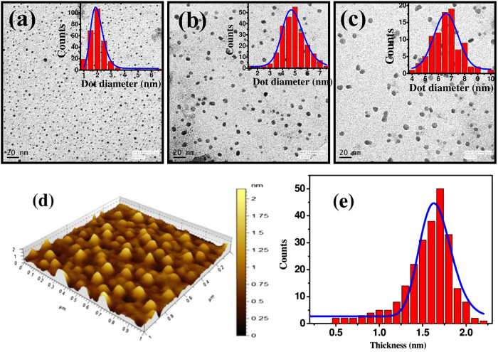
Variable sized MoS2 quantum dots have been synthesized by solvent assisted controlled sonication-centrifugation process. Figure 1(a–c) present the TEM micrographs of the QDs grown with a centrifugation speed of 15000, 14000 and 12000 rpm, respectively. All micrographs reveal the formation of well dispersed and nearly circular quantum dots. Corresponding inset histograms exhibits the size distribution of MoS2 QDs synthesized with a centrifugation speed of 15000, 14000 and 12000 rpm, respectively. The corresponding average size of QDs is extracted to be ~2, ~5 and ~7 nm, respectively. The morphology and height of as-prepared MoS2 QDs have been studied by atomic force microscopy. Typical 3-D surface topographic image with a corresponding histogram of the height distribution of spin coated MoS2 QDs synthesized using a centrifugation speed 15000 rpm are depicted in Fig. 1(d,e). Figure 1(d) indicates almost uniform and narrow size distribution of MoS2 QDs with an average thickness of ~1.8 nm. The average thickness corresponds to the 2–3 layers of MoS2.
Figure 1.
TEM micrographs of synthesized MoS2 quantum dots using centrifugation speeds of (a) 15000, (b) 14000 and (c) 12000 rpm. Corresponding inset exhibits the size distribution of quantum dots with fitted curves (blue line) presented for a different centrifugation speed. (d) Typical atomic force 3D topographic micrograph of MoS2 quantum dots synthesized using a centrifugation speed of 15000 rpm and coated onto a Si substrate. Scale represents height variation along z-axis. (e) Histogram obtained from the corresponding image, representing the thickness distribution of QDs on a Si substrate.
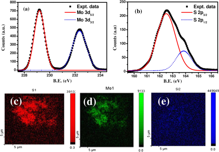
The chemical bonding and composition of as-synthesized MoS2 QDs have been studied by X-ray photoelectron spectroscopy (XPS) using Al–Kα radiation of energy 1486.6 eV. High-resolution core-level XPS spectra showing the binding energy of Mo 3d and S 2p electrons are presented in Fig. 2(a,b), respectively. Two distinct peaks for Mo 3d electrons observed at 229.2 and 232.3 eV are attributed to 3d5/2 and 3d3/2 chemical states, respectively. The spectrum for S 2p electrons is deconvoluted into two well resolved Gaussian peaks located at 162.5 and 163.8 eV, owing to S 2p3/2 and S 2p1/2 states, respectively. The observed peak positions of spin-orbit coupled Mo 3d and S 2p electrons are in excellent agreement with those reported in literature27,28, confirming the synthesis of pure 2-H phase MoS2. The atomic percentage ratio of Mo and S in MoS2 QDs has been estimated by considering the atomic sensitivity factor and area under the S 2p and Mo 3d peaks with Shirley background correction. The atomic ratio of S to Mo is extracted to be 2.12, indicating the formation of a slight S-rich MoS2. A broad energy XPS survey spectrum is presented in Figure S1 (ESI copy), showing a weak but distinct signal of Cl 2p electrons, in addition to O and C as surface contaminants. The presence of Cl as an impurity nominally induces an n-type doping in MoS2 samples13,29. Figure 2(c–e), respectively, present the Auger electron spectroscopic (AES) elemental mapping images of S, Mo and Si atoms for MoS2 QDs deposited on Si. The individual elemental map reveals the homogeneous distribution of two different elements (Mo and S), which are present only at the specific areas of MoS2 layers on Si surface.
Figure 2.
High-resolution XPS spectra showing the binding energy of (a) Mo 3d and (b) S 2p electrons. Scanning auger electron spectroscopy (AES) images of MoS2 films deposited on Si substrates mapping the elemental distribution for (c) Mo, (d) S and (e) Si recorded in the same region.
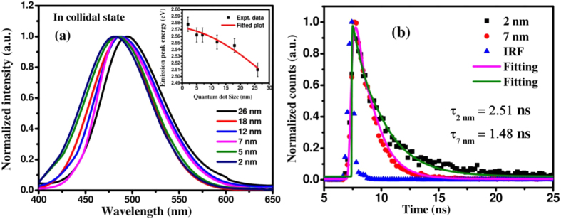
Figure 3(a) exhibits typical photoluminescence spectra of colloidal MoS2 QDs in DMF solvent for different diameters revealing the emission peak in the range of ~480–500 nm for the size varying from ~2 to 26 nm. The shift of PL peak energy as a function of QDs size is presented in the inset of Fig. 3(a). The emission peak energy is gradually shifted to a higher energy with the reduction of QDs size, in well agreement with the quantum confinement effect. Quantum confinement effect has a notable influence on the band gap of nanostructures, when their size is comparable or smaller than the excitonic Bohr radius. The excitonic Bohr radius of MoS2 has been estimated to be ~23 nm. [see in ESI copy]. The photocarrier lifetime of generated excitons in MoS2 QDs have been investigated by employing the time-correlated single photon counting spectroscopy (TCSPS) of colloidal MoS2 QDs using a 380 nm pulsed diode laser excitation source. Figure 3(b) exhibits the typical PL decay spectra of 2 nm and 7 nm dia QDs, along with the instrument response function (IRF). To compare the photogenerated carrier lifetime upon excitation, the experimental data have been fitted, using Marquardt-Levenberg algorithm. All the spectra can be fitted (solid lines) reasonably with a single exponential decay equation, convoluted with a Gaussian IRF described by the equation30:
Figure 3.
(a) Typical PL characteristics of the synthesized QDs in solution exhibiting size tunable emission. Inset of figure (a) shows the variation of peak position as a function of dot diameter. (b) Photoluminescence decay spectra of 2 nm and 7 nm dia MoS2 QDs along with the instrument response function of TCSPS set up. Solid lines are fit to the experimental data using eqn. (1).
 |
where τ is the photon-excited carrier life time and the χ2 value is found to be ~0.98 in the numerical fitting parameter. The well fitted single exponential decay time indicates the existence of only single radiative recombination channel of excitons with negligible contribution from trap states in MoS2 QDs. From the fitting of PL decay curve, the estimated carrier life time is found to be ~1.48 ns and ~2.51 ns, for 7 nm and 2 nm dia QDs, respectively. The larger size QDs exhibits a shorter life time than those of the smaller ones. Therefore with decreasing diameter, the radiative lifetime becomes progressively longer. This is a direct experimental evidence of the temporal stability of photoexcited charge carriers in MoS2 QDs. The observed exciton lifetime is found to be much superior compared to the complex multi-exponential carrier lifetime of ~10 ps observed for layered MoS2 structure31,32. The presence of lower defect density is also consistent with a much higher PL quantum yield of QDs than that of monolayered MoS2 (~10−3) sheet.
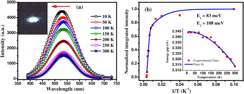
To explore the origin of PL emission, the temperature dependent PL measurements of ~2 nm dia MoS2 QDs have been carried out in the temperature range 10 K to 300 K and the results are depicted in Fig. 4(a). With decreasing temperature, the observed PL peak (~2.31 eV) intensity is enhanced and a slight but distinguishable and progressive blue shift is noticed. Inset is a photograph of white colour PL emission from MoS2 QDs/Si, which instigates to make an LED device. The temperature dependent integrated PL intensity for the ~2 nm dia MoS2 QDs is presented in Fig. 4(b). The PL intensity as a function of inverse temperature has been fitted using the relation33,
Figure 4.
(a) Typical temperature dependent photoluminescence spectra of MoS2 QDs showing the enhancement of emission intensity at lower temperatures. Optical image of the photoluminescence captured for the MoS2/Si heterojunction. (b) Temperature dependent integrated PL intensity of the synthesized QDs of size ~2 nm. The solid line shows the best fitted curve for the experimental data with two activation energies. Inset shows the temperature dependent energy gap for ~2 nm size QDs sample, where the solid line represents the fitting of the experimental data using Varshni’s relation.
 |
where I(T) is the integrated PL intensity at a particular temperature T, ‘A’ and ‘B’ are constants indicating the ratio of nonradiative to radiative recombination probabilities. The activation energy E1 and E2 implies the non-radiative recombination for thermal quenching at a higher temperature. From the best fitting of the data using above equation, thermal activation energies E1 and E2 for PL quenching are found to be 3.24 meV and 59.95 meV, respectively. This indicates that the solution processed MoS2 QDs have a few surface states, due to the local deviation from stoichiometry. This is corroborated by XPS and AES results showing S-rich MoS2 on the surface of quantum dots. Therefore, the observed PL quenching at higher temperature with an activation energy of ~3 meV may be associated with the detrapping of localized charge carriers due to the slight band offset between the core and the surface states of the QDs. The higher activation energy of ~60 meV is related to the dissociation of photo-generated excitons through nonradiative recombination centers. The inset of Fig. 4(b) shows the PL peak shift as a function of temperature. The variation of peak position with temperature has been fitted by Varshni’s equation34, describing the band gap reduction with temperature for semiconductors.
 |
where Eg(0) is the direct band gap energy at 0 K, α is constant, and β is the Einstein temperature for MoS2. The values of α and β are found to be 0.0036 and 10233 K, respectively. The well fitted curve indicates the direct bandedge transition in quantum confined MoS2 dots.
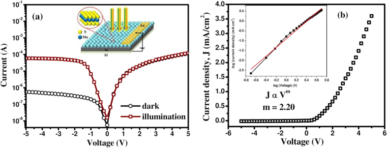
To demonstrate the potential of Si CMOS compatible devices, p-n heterostructures using MoS2 quantum dots of variable diameter have been fabricated on p-Si substrates. The XPS survey scan has shown the incorporation of Cl as an impurity, which results in an n-type doping of MoS2. The efficiency of n-MoS2/p-Si heterojunction for applications in light emitting devices (LED) and photodetectors has been studied. Typical current-voltage (I–V) characteristic of n-MoS2/p-Si heterojunction under dark and illumination conditions is depicted in Fig. 5(a), with the inset showing the device structure. The asymmetric nature of the dark I–V characteristics clearly indicates the formation of a good quality p-n junction at the interfaces with a fairly low dark current (~4.10 × 10⁻⁷ A at −3 V). Upon illumination (514 nm) a photo-to-dark current ratio of ~132 is achieved. The current density (J) versus voltage (V) characteristics of the fabricated heterojunction is shown in Fig. 5(b), which has been fitted with Richardson-Schottky diode equation. The estimated diode ideality factor of the fabricated heterojunction is found to be ~9. The relatively large ideality factor originates due to the existence of high density interfacial defects states in solution processed QDs layer over p-Si resulting in thermal generation-recombination current. The log-log plot of J–V characteristic for the MoS2/Si vertical heterojunction is best fitted with the equation J ∝Vm, which is shown in the inset of Fig. 5(b). The slope m ~2.2, clearly reveals that the charge transport across the p-n junction could be explained by a model described by the charge trapping at the interfacial defect sites, which limit the output current.
Figure 5.
(a) Current-voltage characteristics of fabricated heterojunction, using ~2 nm MoS2 quantum dots on Si, under dark and illumination condition. The inset shows the schematic structure of the heterojunction device. (b) J–V characteristics of fabricated p-n heterojunctions under dark condition, at room temperature. The inset shows the logarithmic J–V curve for the heterojunction fitted with a power law J ∝Vm corresponding to the trap-charge-limited current transport.
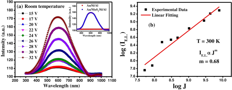
The electroluminescence (EL) characteristics of the fabricated MoS2/Si heterojunction for applications in LED devices have been studied in forward bias condition using Al-doped ZnO (AZO) as the transparent top electrode. A bluish-white light emission could be observed by the naked eye, when sufficient current is injected across the device at room temperature. The EL spectra of MoS2-Si vertical heterostructure are presented under different applied bias and current injection (~0.22–1.98 mA/cm2) in Fig. 6(a). For a comparative study, we have tested the control device without MoS2 QDs, under an applied bias of 30 V. A comparison of the EL emission intensity of control (Au/Si/Al) and the fabricated heterojunction (Au/MoS2/Si/Al) devices is depicted in the inset of Fig. 6(a). The absence of EL emission from the control device unambiguously establishes the importance of p-Si/n-MoS2 heterojunction for achieving the visible-light LED. A broad band spectrum from 450 to 800 nm covering the full visible range indicates the white light emission from MoS2/Si heterojunction. A detectable EL emission is observed above a threshold carrier injection around ~0.2 mA/cm2 and increases continuously with the increase of current across the junction (up to ~2 mA/cm2), as shown in Fig. 6(b). The applied voltage for fairly detectable emission is rather high in agreement with the reported value (~12 V) in the literature35. A higher threshold bias compared to the conventional semiconductor device is owing to the high resistance of nominally undoped MoS2 QDs leading to a low injection current density. The emission peak centered at around ~580 nm is in close agreement with the PL spectra. The integrated EL intensity (IEL) versus injected current density characteristics is found to obey a power law (IEL ∝ Jn), where the exponent “n” accounts for the influence of defects in the light emission characteristics. The exponent value extracted through the linear fitting of the log−log plot of IEL versus J in Fig. 6(b) is found to be ~0.68 for 300 K, is comparable to the reported values in literature36. This sub-linear dependence of integrated EL intensity on injected current is attributed to the presence of non-radiative recombination centers at the interface of Si and MoS2, which also lead to a high dark current density. The stability of the fabricated LEDs has been tested over a wide range of temperatures from 10 to 350 K and the results are presented in Figure S2 (ESI copy). Only a slight decrease in EL intensity is observed with increasing the temperature from 10 to 350 K, indicating the potential of heterojunction LED operating at an elevated temperature. The results indicate the potential of lithography-free, solution processed MoS2 QDs for the fabrication of large-area white light emitting devices on existing Si platforms.
Figure 6.
(a) Bias dependent electroluminescence spectra of MoS2/Si heterojunction recorded at room-temperature. EL characteristics of the control device (without MoS2 quantum dots and MoS2/Si heterojunction are shown in the inset for comparison. (b) The integrated EL intensity fitted against the current density with a power law.
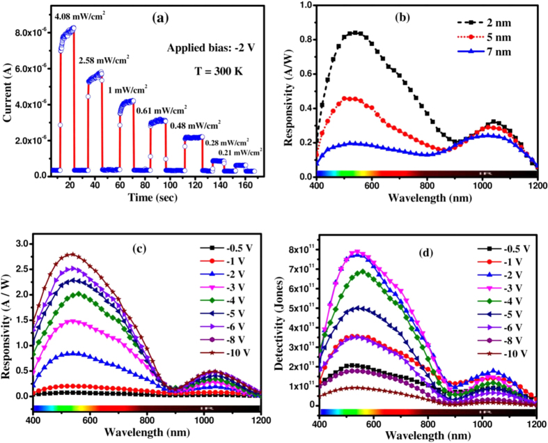
The MoS2/Si heterojunction has also been used to demonstrate the photodetection in reverse bias condition. Figure 7(a) exhibits the temporal time response of the heterojunction detector upon pulsed optical excitation (λ = 514 nm) with varying illumination intensity at an applied bias of −2 V at room temperature. The device current increases sharply and stabilizes in a high conductivity state (ON state) upon illumination and switches back quickly to a lower conductivity state (OFF state) in dark condition. Responsivity (R), detectivity (D) and external quantum efficiency (EQE) are the important parameters to characterize the performance of a photodetector. The spectral responsivity of a photodetector is directly proportional to the internal gain showing the response of the device towards the incident radiation and can be expressed by37:
Figure 7.
(a) Optical modulation characteristics of the fabricated MoS2/Si heterojunction device (using ~2 nm QDs) upon pulsed illumination (514 nm) for variable input intensity at room temperature. (b) Size dependent spectral responsivity of the fabricated heterojunction for different MoS2 QD size, recorded at a bias of −2 V and optical power of 50 μW. (c) Bias dependent response of the device fabricated using QDs of average size ~2 nm. (d) Detectivity in the broadband spectral range of fabricated photodetectors of QD size ~2 nm for different bias.
 |
where, Jph(λ) is the photocurrent density and Popt(λ) is the optical power density for a specific wavelength. Figure 7(b) presents the spectral responsivity of the fabricated heterojunction devices using different sized MoS2 QDs recorded at −2 V bias. The broad spectral response from visible to near-IR consists of two prominent peaks centered around 550 nm and 1030 nm. The peak centered at ~550 nm is attributed to the photo-absorption in MoS2 QDs and the one at ~1030 nm is associated with the intrinsic band-edge transition of Si. It is interesting to note that the responsivity due to QDs increases significantly with the reduction of QD size, as shown in the Fig. 7(b). On the other hand, responsivity due to absorption in Si remains same. The results are in corroboration with the transient PL study (Fig. 3(b)), where the smaller QDs exhibited higher carrier lifetime resulting in a higher detector gain. The higher surface recombination rate results in a lower responsivity for larger sized QDs. The observed peak responsivity for ~2 nm dia MoS2 QDs is significantly higher than the graphene/Si vertical heterostructure (~200 mA/W)38,39 as well as commercial Si (~600 mA/W)40,41 photodetectors.
The influence of applied electric field on photocurrent collection efficiently of fabricated device is shown in Fig. 7(c). The peak responsivity centered at ~550 nm due to MoS2 QDs is enhanced significantly with increasing applied electric field, as compared to that of Si. The EQE spectra as a function wavelength for different QDs diameter is also studied and presented in Figure S3(a) (ESI copy), which also enhanced with reduction of QD sizes. The figure of merit of a photodetector is determined in terms of specific detectivity (D*) and noise equivalent power (NEP), which can be expressed as37,
 |
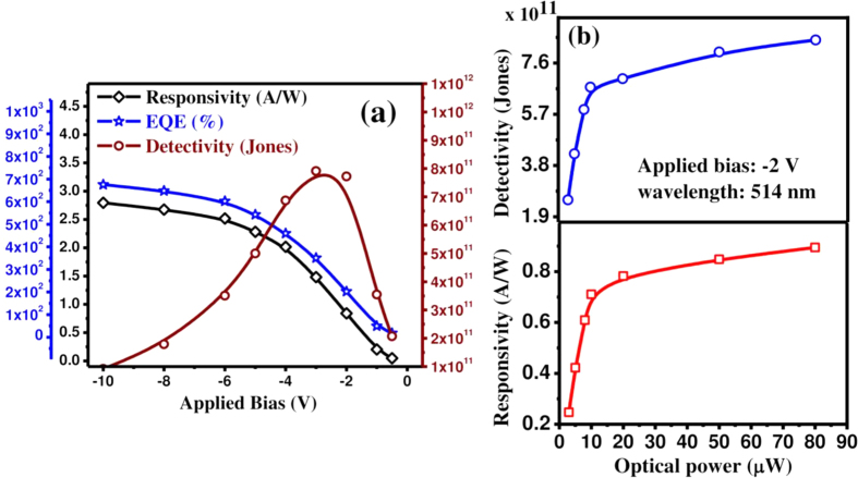
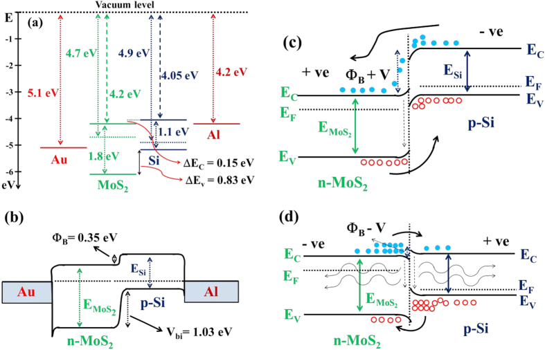
where D* is measured in cm.Hz1/2.W−1 (Jones), A the effective detector area in cm2, R the responsivity, Id the dark current and q is the electronic charge. We assume that the shot noise from dark current is the dominant source of the total noise in comparison to Johnson and flicker noise, which are mainly attributed to thermal fluctuations. Figure 7(d) exhibits the specific detectivity of the heterojunction using 2 nm dia MoS2 QDs in broad wavelength range for different bias. The peak detectivity of the fabricated p-n heterojunction diode is estimated to be ~7 × 1011 cm-Hz1/2.W−1 (or jones) for −2 V bias. The detectivity has also been estimated for variable size MoS2 QDs over the spectral range of 400–1200 nm and is depicted in Figure S3(b) (ESI copy). The detectivity is found to be enhanced by 4-fold as the QDs diameter reduces from ~7 nm to ~2 nm. Peak spectral responsivity, external quantum efficiency (EQE) and detectivity are plotted together against applied reverse bias for the device with 2 nm dia MoS2 QD and the results are presented in Fig. 8(a). As the applied voltage across the p-n junction increases, the responsivity as well as EQE increase sublinearly, but a noticeably different phenomenon is observed for the detectivity. As the bias increases from 0 V, the detectivity increases up to the peak value of ~8 × 10¹¹ Jones and thereafter reduces with the further increase of applied bias. Therefore the detector performance has been found to be optimum at a bias of −2 V for the fabricated MoS2/Si heterostructures. We also examined the responsivity and detectivity of fabricated devices for variable incident optical power and results are depicted in Fig. 8(b). Both the responsivity and detectivity increase linearly for the low illumination power, but exhibit a sub-linear dependence at higher power levels. The increase of illumination intensity leads to the enhanced electron–hole pair generation rate, resulting in a higher photocurrent. However, a sub-linear behavior of the responsivity indicates that the optical response is also affected by the localized trapping and recombination of charge carriers near the band edges. The responsivity and detectivity of the present MoS2 QD/Si heterostructure device were compared with those reported in the literature for similar type photodetectors and are presented in Table 1. The mechanisms of the operation of QD-based photodetectors and LEDs can be explained by the help of energy band diagrams, as shown in Fig. 9. The conduction and valence band edges of Si and MoS2 and the work function edges of Au and Al are aligned in proper energy scale, as shown in Fig. 9(a), resulting in a type-II heterojunction band alignment. Figure 9(b) exhibits the band diagram of the Au/MoS2/Si/Al heterojunction under an equilibrium condition (zero bias). A large barrier potential is created at the Si/QDs interface, when the junction is formed between p-type Si with a work function (ΦSi) of 4.9 eV and n-type MoS2 QDs (ΦMoS2 ~ 4.7 eV). In quantum dot based device, the photo generated charge carriers are transported by the hopping mechanism via interparticle barriers. Upon irradiation with energy larger than the band gap, excitons are generated at the p-n junction. Owing to edge defects of small sized QDs and the potential arising at the interface, the excitons are likely to be dissociated at the interface, and the electrons and holes start drifting towards the opposite electrodes in the presence of electric field, resulting in the photocurrent. With increase in reverse bias, the corresponding electric field across the depletion region is gradually enhanced, resulting in an expansion of the barrier potential as well as the depletion region, as shown in Fig. 9(c). Then enhanced transport of the photoexcited carriers leads to the higher responsivity. Under the application of a forward bias, charge carriers are injected across the junction, resulting in favorable electron-hole recombination. This leads to the visible light emission through radiative recombination of charge carriers injected into the Si/MoS2 heterojunction, which could be explained using the proposed energy band diagram under a forward bias, as shown in Fig. 9(d). At the forward bias condition, the barrier potential at the interface becomes lower which is ideal for the efficient injection of electrons from MoS2 and holes from p-Si. The increase of bias leads to the enhanced charge carrier transport rate and the resultant light emission intensity. The results indicate the potential of MoS2 QD/Si heterojunction for application in high performance multifunctional optoelectronic devices.
Figure 8.
(a) Combined plots of peak responsivity, EQE and detectivity of MoS2 QD (~2 nm)/Si heterojunction photodetector as a function of applied bias. (b) Responsivity and detectivity behavior as a function of illuminated optical power for a fixed wavelength (514 nm) and an applied bias (−2 V).
Table 1. Comparison of the performance of MoS2 and heterojunction based photodetectors.
| Device | Responsivity (A/W) | Detectivity (Jones) | References |
|---|---|---|---|
| Mechanically exfoliated MoS2 flakes | 0.1155 | 1010 | 45 |
| CVD grown MoS2 film | 0.001 | Not reported | 47 |
| RF sputtered MoS2 film | 1.8 | 2 × 10⁹ | 48 |
| Si based photodetector | 0.4 A/W*0.60.59 | 1.55 × 10¹⁰ | *commercial Si- detector, Newport, Model 818-BB-214041 |
| Si-MoS2heterojunction | 70.04 | 1010 | 18 |
| Graphene–silicon heterojunction | 0.2250.210.13 | 2.1 × 10⁸ | 50 |
| Graphene–MoS2 junction | 0.221.26~10 | 4.2 × 10¹⁰ | 51 |
| MoS2 QD/Si heterostructure | 2.8 | 0.8 × 10¹² | This work |
Figure 9.
(a) Estimated band edge alignment of Au, n-MoS2, p-Si and Al to realize the band diagram of type-II heterojunction. Energy band diagram of the fabricated Au/n-MoS2/p-Si/Al heterojunction under (b) equilibrium (zero bias), (c) reverse bias and (d) forward bias conditions.
Conclusions
We have demonstrated the multifunctional optoelectronic devices using vertical heterojunctions of colloidal MoS2 quantum dots integrated on a Si platform. XPS spectra have shown the formation of nearly stoichiometric 2H phase MoS2 with nominal n-type doping due to the presence of Cl. The size of the quantum dots using solvent assisted sonication-centrifugation process could be varied from 2–26 nm exhibiting size tunable emission. Time resolved PL study shows the existence of single radiative recombination centres of MoS2 QDs with superior carrier life time (1.5–2.5 ns), as compared to MoS2 flakes (~10 ps). The fabricated 0D/3D heterostructures exhibit rectifying characteristics with a relatively high junction ideality factor of ~9.0. Bias dependent electroluminescence in the broad spectral range (450–800 nm) of the heterojunction in the forward bias condition shows its efficacy for the LED applications. The spectral responsivity due to MoS2 quantum dots is found to be significantly enhanced with the reduction of size, exhibiting a peak responsivity of 0.85 A/W and a peak detectivity of ~8 × 10¹¹ Jones at −2 V for ~2 nm dia quantum dots. The reported values are much higher than that of commercial Si homojunction, graphene/Si heterojunction and colloidal graphene/carbon dot based devices. The study shows the potential of colloidal n-MoS2 QDs for Si compatible large area multifunctional optoelectronic devices using 0D/3D heterojunctions.
Methods
MoS2 quantum dots were synthesized using the solvent assisted sono-chemical exfoliation process reported previously41,42,43,44. Since the present investigations have been focused on the fabrications of vertical Si/MoS2 p-n heterojunction, a continuous film over clean Si surface is essential. But, it has been observed that the high boiling (~155 °C) dimethylformamide (DMF) leads to the self-aggregation of QDs resulting in a sporadic film. To transfer the QDs from DMF to a suitable solvent for ease of device fabrication, the exfoliation process was modified. After the prolong sonication, the DMF dispersions of MoS2 was vigorously stirred for 2 days to get the homogeneous dots size distribution confirmed by microscopic measurement. Subsequently, MoS2 QDs precipitates of different size were obtained through gradual centrifugation after sonication. All the precipitates were collected separately and a mild heat treatment (at ~60 °C) was performed under the argon (Ar) atmosphere to evaporate the excessive solvent. Finally, all the dried precipitations were redispersed into ethanol, spin coated onto the H-passivated Si surface and dried at room temperature to make a continuous film. The B-doped Si substrates (p-type) with a resistivity of 0.77 Ω-cm were used. Device fabrication was completed by the thermal evaporation of Au (~70 nm) as top electrode and Al (~80 nm) at the backside of Si for bottom electrode, with base pressure of ~1 × 10⁻⁶ torr. However, for LED fabrication, approximately 20 nm of transparent and conducting Al-doped ZnO (AZO) film, was deposited by pulsed laser deposition (PLD) system using a KrF excimer laser (λ = 248 nm, τ = 25 ns) under an optimized condition (base pressure ~5 × 10⁻⁶ Torr, substrate temperature ~300 °C, energy density of ~2 J/cm2 and repetition rate ~5 Hz). The deposited AZO film had a resistivity of ~10−3 Ω.cm and an average transmittance of ~92% in the visible wavelength. Surface morphology of the MoS2 QDs was studied using field emission scanning electron microscopy (FESEM), transmission electron microscopy (TEM) and atomic force microscopy (AFM). The chemical composition and valence states were studied using X-ray photoelectron spectroscopy (XPS) system. The optical absorption spectra of the MoS2 QDs were recorded using an ultraviolet-visible spectrophotometer. Temperature dependent photoluminescence and electroluminescence spectra were recorded using TRIAX-320 monochromator and Hamamatsu R928 PMT detector combination and a He-Cd laser as an excitation source (325 nm). The current-voltage (I–V) characteristics of the fabricated p-n junction and photo-current response of the device was measured using a set-up consisting of a monochromator, calibrated broadband light source and a Keithley semiconductor parameter analyzer (Model 4200-SCS). The temporal response of the PD was recorded using an Ar laser (514 nm) source with a mechanical chopper.
Additional Information
How to cite this article: Mukherjee, S. et al. Novel Colloidal MoS2 Quantum Dot Heterojunctions on Silicon Platforms for Multifunctional Optoelectronic Devices. Sci. Rep. 6, 29016; doi: 10.1038/srep29016 (2016).
Supplementary Material
Acknowledgments
This work was partially supported by the “GBH” project sponsored by Council of scientific and industrial Research (CSIR) and “SER” Project under Department of Science and Technology (DST), Govt. of India, at IIT Kharagpur. The XPS facility of the Dept. of Physics under FIST project is gratefully acknowledged.
Footnotes
Author Contributions S.M. synthesized the quantum dots and performed the characterization and photodetector measurements. R.M. performed the PL measurements. S.M. and A.K.K. worked on the device fabrication and LED measurements. S.M. and S.K.R. analyzed the data and wrote the manuscript. S.D. contributed to the preparation of the manuscript. All authors have given approval to the final version of the manuscript.
References
- Huang X., Zeng Z. Y. & Zhang H. Metal Dichalcogenide Nanosheets: Preparation, Properties and Applications. Chem. Soc. Rev. 42, 1934–1946 (2013). [DOI] [PubMed] [Google Scholar]
- Wang Q. H., Kalantar-Zadeh K., Kis A., Coleman J. N. & Strano M. S. Electronics and optoelectronics of two-dimensional transition metal dichalcogenides. Nat. Nanotech. 7, 699–712 (2012). [DOI] [PubMed] [Google Scholar]
- Jariwala D., Sangwan V. K., Lauhon L. J., Marks T. J. & Hersam M. C. Emerging Device Applications for Semiconducting Two-Dimensional Transition Metal Dichalcogenides. ACS Nano. 8, 1102–1120 (2014). [DOI] [PubMed] [Google Scholar]
- Nicolosi V., Chhowalla M., Kanatzidis M. G., Strano M. S. & Coleman J. N. Liquid Exfoliation of Layered Materials. Science 340, 1226419 (2013). [Google Scholar]
- Chhowalla M., Liu Z. & Zhang H. Two-Dimensional Transition Metal Dichalcogenide (TMD) Nanosheets. Chem. Soc. Rev. 44, 2584–2586 (2015). [DOI] [PubMed] [Google Scholar]
- Huang X., Tan C., Yin Z. & Zhang H. 25th Anniversary Article: Hybrid Nanostructures Based on Two-Dimensional Nanomaterials. Adv. Mater. 26, 2185–2204 (2014). [DOI] [PubMed] [Google Scholar]
- Li H., Wu J., Yin Z. & Zhang H. Preparation and Applications of Mechanically Exfoliated Single-Layer and Multilayer MoS2 and WSe2 Nanosheets. Acc. Chem. Res. 47, 1067–1075 (2014). [DOI] [PubMed] [Google Scholar]
- Mak K. F., Lee C., Hone J., Shan J. & Heinz T. F. Atomically thin MoS2: a new direct-gap semiconductor. Phys. Rev. Lett. 105, 136805 (2010). [DOI] [PubMed] [Google Scholar]
- Splendiani A. et al. Emerging Photoluminescence in Monolayer MoS2. Nano Lett. 10, 1271–1275 (2010). [DOI] [PubMed] [Google Scholar]
- Lopez-Sanchez O., Lembke D., Kayci M., Radenovic A. & Kis A. Ultrasensitive photodetectors based on monolayer MoS2. Nat. Nanotech. 8, 497–501 (2013). [DOI] [PubMed] [Google Scholar]
- Radisavljevic B., Radenovic A., Brivio J., Giacometti V. & Kis A. Single-Layer MoS2 Transistors. Nat. Nanotech. 6, 147–150 (2011). [DOI] [PubMed] [Google Scholar]
- Yin Z. et al. Single-Layer MoS2 Phototransistors. ACS Nano. 6, 74–80 (2012). [DOI] [PubMed] [Google Scholar]
- Gong Y. et al. Vertical and in-plane heterostructures from WS2/MoS2 monolayers. Nat. Mater. 13, 1135–1142 (2014). [DOI] [PubMed] [Google Scholar]
- Ceballos F., Bellus M. Z., Chiu H. Y. & Zhao H. Ultrafast Charge Separation and Indirect Exciton Formation in a MoS2/MoSe2 van der Waals Heterostructure. ACS Nano. 8, 12717–12724 (2014). [DOI] [PubMed] [Google Scholar]
- Deng Y. et al. Black Phosphorus Monolayer MoS2 van der Waals Heterojunction p-n Diode. ACS Nano. 8, 8292–8299 (2014). [DOI] [PubMed] [Google Scholar]
- Tsai M. L. et al. Monolayer MoS2 Heterojunction Solar Cells. ACS Nano. 8, 8317–8322 (2014). [DOI] [PubMed] [Google Scholar]
- Lopez-Sanchez O. et al. Light Generation and Harvesting in a van der Waals Heterostructure. ACS Nano. 8, 3042–3048 (2014). [DOI] [PMC free article] [PubMed] [Google Scholar]
- Li Y., Xu C. Y., Wang J. Y. & Zhen L. Photodiode-like behavior and excellent photoresponse of vertical Si/monolayer MoS2 heterostructures. Sci Rep. 26, 7186 (2014). [DOI] [PMC free article] [PubMed] [Google Scholar]
- Li X., Rui M., Song J., Shen Z. & Zeng H. Carbon and Graphene Quantum Dots for Optoelectronic and Energy Devices: A Review. Adv. Funct. Mater. 25, 4929–4947 (2015). [Google Scholar]
- Zhang X. et al. Color-Switchable Electroluminescence of Carbon Dot Light-Emitting Diodes. ACS Nano. 7, 11234–11241 (2013). [DOI] [PubMed] [Google Scholar]
- Jin Z., Owour P., Lei S. & Ge L. Graphene, graphene quantum dots and their applications in optoelectronics. Current Opinion in Colloid & Interface Science. 20, 439–453 (2015). [Google Scholar]
- Konstantatos G. et al. Hybrid graphene–quantum dot phototransistors with ultrahigh gain. Nat. nanotech. 7, 363–368 (2012). [DOI] [PubMed] [Google Scholar]
- Li L. S. & Yan X. Colloidal Graphene Quantum Dots. J. Phys. Chem. Lett. 1, 2572–2576 (2010). [Google Scholar]
- Zhang Q. et al. Solution-Processed Graphene Quantum Dot Deep-UV Photodetectors. ACS Nano. 9, 1561–1570 (2015). [DOI] [PubMed] [Google Scholar]
- Park H. et al. Large Scale Synthesis and Light Emitting Fibers of Tailor-Made Graphene Quantum Dots. Sci. Rep. 5, 14163 (2015). [DOI] [PMC free article] [PubMed] [Google Scholar]
- Lin H. et al. Colloidal synthesis of MoS2 quantum dots: size-dependent tunable photoluminescence and bioimaging. New J. Chem. 39, 8492–8497 (2015). [Google Scholar]
- Kibsgaard J., Chen Z., Reinecke B. N. & Jaramillo T. F. Engineering the surface structure of MoS2 to preferentially expose active edge sites for electrocatalysis. Nat. Mater. 11, 963–969 (2012). [DOI] [PubMed] [Google Scholar]
- Jin Z., Shin S., Kwon D. H., Han S. J. & Min Y. S. Novel chemical route for atomic layer deposition of MoS2 thin film on SiO2/Si substrate. Nanoscale 6, 14453–14458 (2014). [DOI] [PubMed] [Google Scholar]
- Sundaram R. S. et al. Electroluminescence in Single Layer MoS2. Nano Lett. 13, 1416–1421 (2013). [DOI] [PubMed] [Google Scholar]
- Yuan L. & Huang L. Exciton dynamics and annihilation in WS2 2D semiconductors. Nanoscale. 7, 7402–7408 (2015). [DOI] [PubMed] [Google Scholar]
- Korn T., Heydrich S., Hirmer M., Schmutzler J. & Schüller C. Low-temperature photocarrier dynamics in monolayer MoS2. Appl. Phys. Lett. 99, 102109 (2011). [Google Scholar]
- Lagarde D. et al. Carrier and Polarization Dynamics in Monolayer MoS2. Phy. Rev. Lett. 112, 047401 (2014). [DOI] [PubMed] [Google Scholar]
- Palm J., Gan F., Zheng B., Michel J. & Kimerling L. C. Electroluminescence of erbium-doped silicon. Phy. Rev. B. 54, 17603 (1996). [DOI] [PubMed] [Google Scholar]
- Varshni Y. P. Temperature dependence of the energy gap in semiconductors. Physica. 34, 149–154 (1967). [Google Scholar]
- Yin Z. et al. Preparation of MoS2–MoO3 Hybrid Nanomaterials for Light-Emitting Diodes. Angew. Chem. Int. Ed. 126, 12768–12737 (2014). [DOI] [PubMed] [Google Scholar]
- Katiyar A. K., Sinha A. K., Manna S. & Ray S. K. Fabrication of Si/ZnS Radial Nanowire Heterojunction Arrays for White Light Emitting Devices on Si Substrates. ACS Appl. Mater. Interfaces. 6, 15007–15014 (2014). [DOI] [PubMed] [Google Scholar]
- Das K., Mukherjee S., Manna S., Ray S. K. & Raychaudhuri A. K. Single Si nanowire (diameter ≤ 100 nm) based polarization sensitive near-infrared photodetector with ultra-high responsivity. Nanoscale 6, 11232–11239 (2014). [DOI] [PubMed] [Google Scholar]
- Maiti R., Manna S., Midya A. & Ray S. K. Broadband Photoresponse and Rectification of Novel Graphene Oxide/n-Si Heterojunctions. Optics express 21, 26034–26043 (2013). [DOI] [PubMed] [Google Scholar]
- Wang X., Cheng Z., Xu K., Tsang H. K. & Xu J. B. High-responsivity graphene/silicon-heterostructure waveguide photodetectors. Nat. Photonics. 7, 888–891 (2013). [Google Scholar]
- Zheng J. P., Jiao K. L., Shen W. P., Anderson W. A. & Kwok H. S. Highly sensitive photodetector using porous silicon. Appl. Phys. Lett. 61, 459–461 (1992). [Google Scholar]
- Ahmad M., Rasool K., Rafiq M. A. & Hasan M. M. Enhanced and persistent photoconductivity in vertical silicon nanowires and ZnS nanoparticles hybrid devices. Appl. Phys. Lett. 101, 223103 (2012). [Google Scholar]
- Gopalakrishnan D., Damien D. & Shaijumon M. M. MoS2 Quantum Dot-Interspersed Exfoliated MoS2 Nanosheets. ACS Nano, 8, 5297–5303 (2014). [DOI] [PubMed] [Google Scholar]
- Štengl V. & Henychab J. Strongly luminescent monolayered MoS2 prepared by effective ultrasound exfoliation. Nanoscale 5, 3387–3394 (2013). [DOI] [PubMed] [Google Scholar]
- Mukherjee S., Maiti R., Midya A., Das S. & Ray S. K. Tunable Direct Bandgap Optical Transitions in MoS2 Nanocrystals for Photonic Devices. ACS Photonics 2, 760–768 (2015). [Google Scholar]
- Zhang X. et al. A Facile and Universal Top-Down Method for Preparation of Monodisperse Transition-Metal Dichalcogenide Nanodots. Angew. Chem. Int. Ed. 54, 5425–5428 (2015). [DOI] [PubMed] [Google Scholar]
- Woong C. et al. High‐detectivity multilayer MoS2 phototransistors with spectral response from ultraviolet to infrared. Adv. Mater. 24, 5832–5836 (2012). [DOI] [PubMed] [Google Scholar]
- Kufer D. et al. G. Hybrid 2D–0D MoS2–PbS quantum dot photodetectors. Adv. Mater. 27, 176–180 (2015). [DOI] [PubMed] [Google Scholar]
- Néstor P. L. et al. CVD-grown monolayered MoS2 as an effective photosensor operating at low-voltage. 2D Materials 1, 011004 (2014). [Google Scholar]
- Ling Z. P. et al. Large-scale two-dimensional MoS2 photodetectors by magnetron sputtering. Optics express. 23, 13580–13586 (2015). [DOI] [PubMed] [Google Scholar]
- Midya A., Ghorai A., Mukherjee S., Maiti R. & Ray S. K. Hydrothermal growth of few layer 2H-MoS2 for heterojunction photodetector and visible light induced photocatalytic applications. J. Mater. Chem. A. 4, 4534 (2016). [Google Scholar]
- An X., Liu F., Jung Y. J. & Kar S. Tunable graphene–silicon heterojunctions for ultrasensitive photodetection. Nano letters 13, 909–916 (2013). [DOI] [PubMed] [Google Scholar]
- Yu W. J. et al. Highly efficient gate-tunable photocurrent generation in vertical heterostructures of layered materials. Nat. nanotech. 8, 952–958 (2013). [DOI] [PMC free article] [PubMed] [Google Scholar]
- Vabbina P. et al. Highly Sensitive Wide Bandwidth Photodetector Based on Internal Photoemission in CVD Grown p-Type MoS2/Graphene Schottky Junction. ACS appl. mater. & inter. 7, 15206–15213 (2015). [DOI] [PubMed] [Google Scholar]
- Xu H. et al. High Responsivity and Gate Tunable Graphene‐MoS2 Hybrid Phototransistor. Small 10, 2300–2306 (2014). [DOI] [PubMed] [Google Scholar]
Associated Data
This section collects any data citations, data availability statements, or supplementary materials included in this article.


