Abstract
Highly sensitive hydrogen detection at room temperature can be realized by employing solution‐processed MoS2 nanosheet–Pd nanoparticle composite. A MoS2–Pd composite exhibits greater sensing performance than its graphene counterpart, indicating that solvent exfoliated MoS2 holds great promise for inexpensive and scalable fabrication of highly sensitive chemical sensors.
Keywords: hydrogen sensing, MoS2 nanosheet, room temperature, solvent exfoliation
Hydrogen, a clean and abundant energy source, has been utilized in fuel cells to generate electricity with the aim of reducing the dependence on fossil fuels. However, hydrogen is a colorless, odorless, tasteless, flammable, and explosive gas, which arises some safety concerns. For the safe implementation of fuel cells, hydrogen leaks have to be detected before hydrogen concentration reaches a hazardous level.1, 2 Metal oxide sensors3, 4, 5, 6 are effective for the detection of hydrogen; however they require high operation temperature, which increases the power consumption as well as posing a risk for safety itself since hydrogen is highly flammable at elevated temperatures.7, 8 In this regard, developing reliable hydrogen detection technologies which can operate at room temperature is highly desirable.
2D materials have drawn tremendous attention in recent years due to their novel and unique electronic, optical, and mechanical properties.9, 10, 11 Moreover, their high surface‐to‐volume ratio makes them attractive for sensing applications. Graphene, a 2D material made of carbon, has been shown to be an effective sensing platform for toxic gases such as NO2 and NH3.12, 13, 14, 15 Decorating graphene with metal nanoparticles (NPs) such as Pt, Pd, Au, or Ag increases the sensor response due to their catalytic effect.16, 17 Moreover, Pd‐decorated graphene has been demonstrated as a hydrogen sensor,18, 19 in which modulation of Pd work function causes a change in the amount of net doping in graphene leading to a resistance change showing a response to hydrogen.
Recently, molybdenum disulfide (MoS2) has been explored for electronic applications due to its sizable band gap (1.2 and 1.8 eV for bulk and single layer, respectively), which enables its conductivity to be modulated by a gate voltage.20, 21 Similar to graphene, MoS2 has a layered structure, where each layer consists of covalently bonded Mo–S atoms and the neighboring layers attach each other by van der Waals forces.22 MoS2 can be obtained by mechanical or chemical exfoliation of bulk MoS2 or can be grown by Chemical Vapor Deposition (CVD).23, 24, 25 Perkins et al. have demonstrated mechanically exfoliated single layer MoS2 flake as a chemical sensor, in which monolayer MoS2 shows a strong response to electron donors (triethylamine) and a lower response to electron acceptors (acetone) with detection limits of 10 ppb (parts per billion) and 500 ppm (parts per million), respectively, attributed to the n‐type nature of MoS2.26 However, mechanical exfoliation is a low yield method and is not suitable for practical applications. On the other hand, CVD grown MoS2 films have also been investigated for the gas sensing and a strong response was found towards NH3 with a detection limit of 300 ppb.27 Although CVD method seems to provide a solution for the scalable growth of MoS2, high temperature growth conditions (750–1000 °C)24, 27 pose a barrier for inexpensive fabrication of chemical sensors.
Chemical exfoliation of MoS2 is favorable for the large scale and low cost production of MoS2 chemical sensors. A lithium intercalation method28 can be used to exfoliate bulk MoS2 crystals to produce single layer MoS2 nanosheets. However, this method requires a long lithiation process (3 days) and results in MoS2 nanosheets with traces of lithium particles, which degrades the MoS2 semiconducting properties.29 On the other hand, solvent exfoliation method30 can provide high yield and fast production of a few layer MoS2 nanosheets, in which exfoliation takes place by ultrasonication of bulk MoS2 in suitable solvents such as N‐methyl‐pyrrolidone (NMP) or isopropanol whose surface tension is in the range of 30–40 mJ m−2, which facilitates the exfoliation process.31, 32
In this work, we present solution‐processed MoS2 nanosheet–Pd nanoparticle composite for H2 sensing at room temperature, in which MoS2–Pd composite show remarkable electrical response towards H2 with excellent response and recovery times. A few‐layers MoS2 nanosheets can be produced by a facile solvent exfoliation method and the MoS2–Pd composite can be fabricated by simply drop casting of MoS2–PdCl2 solution and subsequent annealing process. The effect of annealing time on H2 sensing performance of MoS2–Pd composite is investigated. The sensing mechanism is studied by transport measurements of MoS2 nanosheets and MoS2–Pd composite by fabricating field effect transistor (FET) devices. We also compare the H2 sensing performance of MoS2–Pd composite with graphene–Pd composite, fabricated in a similar fashion, revealing that MoS2–Pd exhibits much higher sensor response with shorter response and recovery times and indicating that 2D MoS2 is a promising candidate for highly sensitive room temperature gas detection.
MoS2–Pd composite was prepared by drop casting of MoS2–PdCl2 solution (Figure 1 a) on SiO2‐coated Si substrates with subsequent annealing process to reduce PdCl2 (see the Experimental Section for details). The optical image of sensor device is shown in Figure 1b. Figure 1c,d shows tilted‐view scanning electron microscopy (SEM) images of the MoS2–Pd composite film, in which MoS2–Pd composite forms a continuous film (around 500 nm thick) in a self‐assembled manner. From the top‐view SEM image (Figure 1e), it is clear that MoS2 nanosheets are highly exfoliated as they appear transparent. In order to further understand the layered structure of MoS2, AFM (Atomic Force Microscopy) measurements and thickness analysis of the MoS2 nanosheets dispersed on a Si substrate were carried out. We measured the thickness of nine MoS2 nanosheets, in which we found that the thickness of the nanosheets range from 2.2 to 25.8 nm, with the majority of them having a thickness less than 10 nm. By considering the thickness of the single layer MoS2 being 0.65 nm, the number of layers is estimated to range from 3 to 40 (Figure S1, Supporting Information). Figure 1f illustrates the schematic diagram of the MoS2–Pd composite, in which Pd NPs (20–100 nm diameter) are sandwiched by MoS2 nanosheets.
Figure 1.
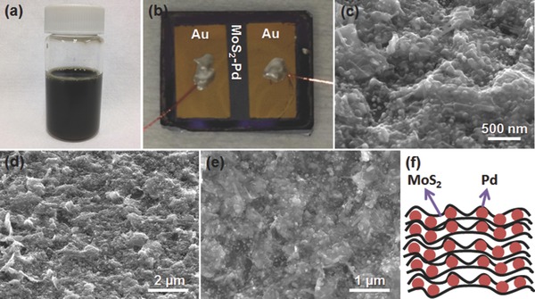
Optical image of a) MoS2–PdCl2 solution and b) MoS2–Pd composite sensor device. c) High and d) low magnification tilted‐view, and e) top‐view SEM images of MoS2–Pd composite. f) Schematic illustration of MoS2–Pd composite.
X‐ray diffraction (XRD) analyses (Figures 2 a and S2, Supporting Information) were carried out in order to evaluate the crystal structure of bulk MoS2 powder, MoS2 nanosheets, and MoS2–Pd composite. XRD pattern of bulk MoS2 powder shows the main peaks of molybdenite‐2H, in which a strong peak is observed at 2θ ≈ 14.4o (002), indicating that MoS2 powder is highly crystalline.33 On the other hand, MoS2 nanosheets and MoS2–Pd composite also showed the (002) peaks with smaller intensities, indicating that MoS2 is highly exfoliated after ultrasonication.34, 35 After exfoliation, the position of the (002) peak slightly shifted to lower angle due to the increased interlayer spacing. Furthermore, we observed that the intensity of the (002) peak is the smallest for MoS2–Pd composite, which can be attributed to the possibility that MoS2 nanosheets are precluded from restacking by Pd NPs. To further analyze MoS2, Raman spectroscopy measurements were performed (Figure 2b), in which the characteristic Raman shifts of MoS2 (E1 2g and A1g)36 were observed for all the samples.
Figure 2.
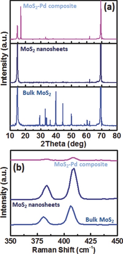
a) XRD patterns and b) Raman spectra of bulk MoS2, MoS2 nanosheets, and MoS2–Pd composite.
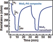
Electrical response of the sensors to H2 was evaluated by flowing H2 in N2 with 200 sccm (standard cubic centimeters per minute) flow rate at room temperature. In our measurements, the effect of N2 on sensor response is strictly eliminated by flowing N2 prior to H2 until the sensor response is stabilized. The MoS2 nanosheets and MoS2–Pd composite show a strong response to N2, which could be explained by the fact that O2 molecules are pushed outside of the chamber by N2 flow, in which p‐doping effect of O2 vanishes. O2 adsorption is known to lead significant hole doping in graphene,37 hence a similar effect can be expected for MoS2. The sensor response is defined as R 1/R 2, where R 1 and R 2 are the resistance of the sensor device in N2 and H2, respectively. Figure 3 a shows the electrical response of MoS2 nanosheets and MoS2–Pd composite to 50 000 ppm of H2, in which MoS2 nanosheets do not show any significant response to H2 exposure (see Figure S3, Supporting Information for the zoomed‐in plot to see the details of response) while MoS2–Pd composite shows a strong response. Pd NPs serve as the sensing material, where the work function of Pd shifts upon H2 exposure due to the formation of PdHx compounds.38 H2 molecules can dissociate on the surface of Pd and diffuse into the Pd lattice changing its work function.39 As a result, the doping amount in MoS2 is altered by changing the overall resistance of the device. The role of 2D MoS2 is crucial since it serves as a platform for the attachment of the Pd NPs and provides high surface‐to‐volume‐ratio and low charge carrier density in the background due to its semiconducting nature, which makes it highly sensitive to H2 exposure. The resistance of MoS2–Pd composite device exhibits a sharp decrease with H2 exposure followed by saturation, with the sensor response being about 10, as well as the sensor shows complete recovery in air without any heating or UV irradiation. Desorption of hydrogen atoms from Pd takes place in the presence of O2 by forming H2O,40 which in turn recovers the sensor. The sensor response and recovery times are defined as the amount of the time required for the sensor resistance to reach 90% of its saturation and to recover to 90% of its ground state, respectively.41 MoS2–Pd composite sensor device has response and recovery times of 40 and 83 s, respectively. I–V measurements were performed before and after H2 exposure (Figure 3b), in which linear I–V responses are obtained. This ensures that no Schottky barrier forms between Ti/Au contacts and MoS2–Pd composite and the channel itself is responsible for the resistance change upon H2 exposure rather than the modulation of Schottky barrier height. We also performed sensing measurements at different concentrations of H2, ranging from 50 000 to 500 ppm by 40 s pulses (Figure 3c). Figure 3d shows the recovery time and sensor response as a function of H2 concentration, in which both the recovery time and sensor response decrease with the decreasing H2 concentration. As the partial pressure of H2 is decreased, the amount of hydrogen uptake into the Pd NPs is reduced resulting in a lower sensor response. The sensor response exhibits almost a linear trend for concentrations of 500–25 000 ppm and tends to deviate to a saturation trend at higher concentrations.
Figure 3.
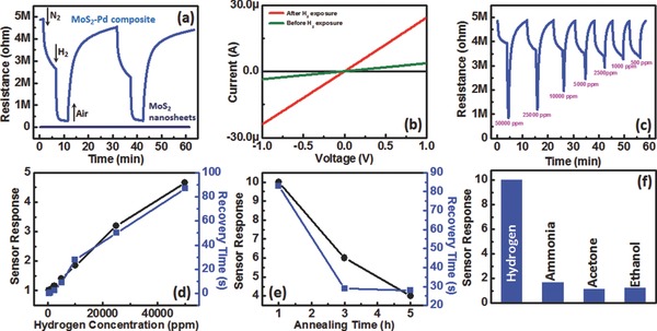
a) Electrical responses of pristine MoS2 nanosheets and MoS2–Pd composite to 50 000 ppm H2. b) I–V characteristics of MoS2–Pd composite before and after H2 exposure. c) Electrical response of MoS2–Pd composite exposed to different concentrations of H2 (500–50 000 ppm) by 40 s pulses. d) Recovery time and sensor response of MoS2–Pd composite as a function of H2 concentration. e) Recovery time and sensor response of MoS2–Pd composite as a function of annealing time. f) Cross‐sensitivity of MoS2–Pd composite to 50 000 ppm hydrogen, 50 ppm ammonia, 50 000 ppm acetone and ethanol.
The effect of annealing time on the sensor characteristics of MoS2–Pd composite was investigated. Figure 3e shows the recovery time and sensor response of the MoS2–Pd composite sensors annealed for various time durations. Increasing the annealing time significantly improves the recovery of the sensor at the expense of reduced sensor response. For example, the recovery times/sensor responses are 83 s/10, 29 s/6, and 28 s/4 for 1, 3, and 5 h annealed samples, respectively. SEM analysis (Figure S4, Supporting Information) of the samples show that annealing changes the morphology of the film into a more spaced structure, which helps the recovery of the sensors. On the other hand, reduced sensor response could be explained by the fact that annealing turns MoS2 nanosheets into a more agglomerated structure resulting in a decrease in the number of Pd NPs which contact to MoS2 nanosheets.
We also investigated the cross‐sensitivity of MoS2–Pd composite to ammonia, ethanol and acetone. As shown in Figure 3f, the sensor exhibits a sensor response of 10, 1.65, 1.13, and 1.22 to 50 000 ppm hydrogen, 50 ppm ammonia, 50 000 ppm acetone and ethanol, respectively, indicating that MoS2–Pd composite has a little cross‐sensitivity to these gases.
As a comparison, we fabricated graphene–Pd composite sensor and measured its electrical response to 50 000 ppm of H2 (Figure S5, Supporting Information), in which graphene–Pd composite (Figure S6, Supporting Information) shows a sensor response of only 1.34 with a response time of 102 s and incomplete recovery in 30 min. Unlike MoS2–Pd, the resistance of graphene–Pd composite increases with H2 exposure indicating that graphene–Pd composite are initially p‐doped and the reduction in the work function of Pd upon H2 exposure leads to partial depletion of holes in graphene increasing its resistance. It is clearly seen that MoS2–Pd composite exhibits superior H2 sensing performance than its graphene counterpart indicating that 2D MoS2 is more promising for room temperature hydrogen detection.
In order to elucidate the sensing mechanism of MoS2–Pd composite, transport measurements were carried out by fabricating FET devices. Figure 4 shows the transport data of MoS2 nanosheets and MoS2–Pd composite, in which MoS2 nanosheets and MoS2–Pd composite both show n‐type transport behavior with a large shift to the positive side in threshold voltage for MoS2–Pd composite. This indicates Pd NPs have a p‐doping effect on MoS2 causing partial depletion of electrons. Based on these results, we believe that work function of Pd is higher than that of MoS2 before H2 exposure, which is consistent with the reported work function values of Pd (5.1–5.6 eV)42, 43 and MoS2 (4.3–5.2 eV).44, 45 After H2 exposure, work function of Pd decreases significantly resulting in a recovery of depleted electrons in MoS2, which in turn reduces the overall resistance.
Figure 4.
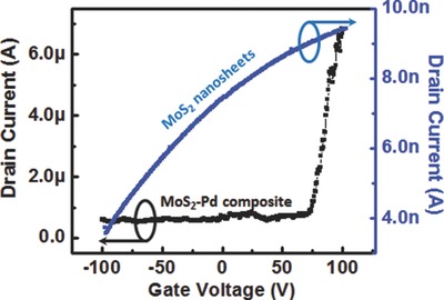
Drain current versus gate voltage of MoS2 nanosheets and MoS2–Pd composite.
In summary, we demonstrated highly sensitive detection of H2 at room temperature by employing solution‐processed MoS2 nanosheet–Pd nanoparticle composite, which can be readily fabricated by a facile solvent exfoliation and drop casting method. In particular, MoS2–Pd composite sensor exhibits a sensor response of around 10 toward 50 000 ppm H2 with a response and recovery time of 40 and 83 s, respectively. Pd NPs enable sensitivity toward H2 based on work function modulation of Pd providing high sensitivity, fast response, and recovery. Recovery time can be further decreased down to 28 s by increasing the annealing time. Furthermore, the sensing performance of MoS2–Pd was compared with graphene–Pd composite film, in which MoS2–Pd outperforms graphene–Pd composite film. These results indicate that chemically exfoliated MoS2 holds a great potential for the inexpensive and scalable fabrication of high sensitivity chemical sensors.
Experimental Section
Materials: Bulk MoS2 powder (5 μm powder size), NMP, and palladium chloride (PdCl2) were purchased from Sigma Aldrich. Bulk graphite flakes were purchased from Graphene Supermarket.
Preparation of MoS2–PdCl2 and Graphene–PdCl2 Solutions: A 400 mg bulk MoS2 powder was mixed with 80 mL NMP and then the mixture was probe sonicated (750 W and 80% amplitude) in an ice bath for 2 h to exfoliate bulk MoS2. The resultant solution was then centrifuged at 1500 rpm for 45 min to remove any remaining bulk particles. After that, NMP was evaporated in a vacuum oven followed by redispersion of MoS2 nanosheets in deionized water with a concentration of 1.5 mg mL−1. MoS2–PdCl2 solution was prepared by adding 30 mg PdCl2 into 20 mL of MoS2–water solution and a subsequent sonication for 30 min. Graphene–PdCl2 solution was prepared by following the same procedure.
Fabrication of Hydrogen Sensors: A 0.5 mL of prepared MoS2–PdCl2 and graphene‐PdCl2 solution was dropped on SiO2‐coated Si substrates, followed by baking on a hot plate at 100 °C until the solution is dried. The resultant film was then annealed in forming gas atmosphere at 400 °C to reduce PdCl2 and remove any remaining NMP. In order to fabricate the contacts for sensing measurements a piece of Teflon tape was used as a mask to define the channel (2 mm channel length and 1 cm width) and subsequent sputter deposition of Ti/Au (10/150 nm) was performed. For the fabrication of MoS2 nanosheet sensors, MoS2 nanosheets which were dispersed in ethanol was spin coated on SiO2‐coated Si substrate and then photolithography and following deposition of Ti/Au (10/150 nm) was performed to fabricate the finger electrodes.
Characterization: XRD measurements were conducted by a Bruker D2 Phaser X‐ray diffractometer (XRD) with Cu Kα (λ = 0.154 nm) as the radiation source. Raman spectroscopy measurements were carried out by a Renishaw raman spectrometer at 514 nm. AFM measurements were performed with a Digital Instruments 3100 microscope under tapping mode.
Sensing Measurements: H2 (50 000 ppm) in N2 was used as a starting gas and it was diluted with N2 to the desired concentrations by using mass flow controllers. For the measurements, target gas was flowed with 200 sccm flow rate through a small glass chamber (10 cm3 volume), where the sensor device is mounted and the resistance was recorded by Keithley multimeter (2100). For ammonia sensing measurements, 50 ppm ammonia gas in N2 was used. For ethanol and acetone sensing measurements, the desired amount of liquid acetone and ethanol (calculated by using ideal gas law) were evaporated in a closed chamber, in which the concentrations of the solvents correspond to 50 000 ppm. For the recovery of the sensors, air was introduced into the chamber.
Fabrication of FET Devices and Transport Measurements: MoS2 nanosheets and MoS2 nanosheet‐PdCl2 dispersed in ethanol were spin coated on a SiO2 (300 nm thick) coated Si (high doped) substrate. A subsequent annealing process at 400 °C in forming gas environment was performed in order to reduce PdCl2. Source and drain electrodes were fabricated by photolithography and subsequent evaporation of Ti/Au (10/150 nm). Transport measurements were conducted by B1500 Agilent semiconductor device analyzer.
Supporting information
As a service to our authors and readers, this journal provides supporting information supplied by the authors. Such materials are peer reviewed and may be re‐organized for online delivery, but are not copy‐edited or typeset. Technical support issues arising from supporting information (other than missing files) should be addressed to the authors.
Supplementary
Acknowledgements
This study was supported by Iwama Endowed Fund at University of California, San Diego.
Kuru C., Choi C., Kargar A., Choi D., Kim Y. J., Liu C. H., Yavuz S., Jin S. (2015). MoS2 Nanosheet–Pd Nanoparticle Composite for Highly Sensitive Room Temperature Detection of Hydrogen. Adv. Sci., 2: 1500004. doi: 10.1002/advs.201500004
References
- 1. Boon‐Brett L., Bousek J., Black G., Moretto P., Castello P., Hübert T., Banach U., Int. J. Hydrogen Energy 2010, 35, 373. [Google Scholar]
- 2. Buttner W. J., Post M. B., Burgess R., Rivkin C., Int. J. Hydrogen Energy 2011, 36, 2462. [Google Scholar]
- 3. Varghese O. K., Gong D., Paulose M., Ong K. G., Grimes C. A., Sens. Actuators, B 2003, 93, 338. [Google Scholar]
- 4. Shukla S., Seal S., Ludwig L., Parish C., Sens. Actuators, B 2004, 97, 256. [Google Scholar]
- 5. Shukla S., Patil S., Kuiry S., Rahman Z., Du T., Ludwig L., Parish C., Seal S., Sens. Actuators, B 2003, 96, 343. [Google Scholar]
- 6. Lin F., Takao Y., Shimizu Y., Egashira M., Sens. Actuators, B 1995, 25, 843. [Google Scholar]
- 7. Hord J., Int. J. Hydrogen Energy 1978, 3, 157. [Google Scholar]
- 8. Kumar R., J. Fire Sci. 1985, 3, 245. [Google Scholar]
- 9. Novoselov K. S., Geim A. K., Morozov S. V., Jiang D., Zhang Y., Dubonos S. V., Grigorieva I. V., Firsov A. A., Science 2004, 306, 666. [DOI] [PubMed] [Google Scholar]
- 10. Ramakrishna Matte H., Gomathi A., Manna A. K., Late D. J., Datta R., Pati S. K., Rao C., Angew. Chem. 2010, 122, 4153. [DOI] [PubMed] [Google Scholar]
- 11. Lee Y., Zhang X., Zhang W., Chang M., Lin C., Chang K., Yu Y., Wang J. T., Chang C., Li L., Adv. Mater. 2012, 24, 2320. [DOI] [PubMed] [Google Scholar]
- 12. Li W., Geng X., Guo Y., Rong J., Gong Y., Wu L., Zhang X., Li P., Xu J., Cheng G., ACS Nano 2011, 5, 6955. [DOI] [PubMed] [Google Scholar]
- 13. Romero H. E., Joshi P., Gupta A. K., Gutierrez H. R., Cole M. W., Tadigadapa S. A., Eklund P. C., Nanotechnology 2009, 20, 245501. [DOI] [PubMed] [Google Scholar]
- 14. Lu G., Ocola L. E., Chen J., Nanotechnology 2009, 20, 445502. [DOI] [PubMed] [Google Scholar]
- 15. Chung M. G., Kim D. H., Lee H. M., Kim T., Choi J. H., Yoo J., Hong S., Kang T. J., Kim Y. H., Sens. Actuators, B 2012, 166, 172. [Google Scholar]
- 16. Gutés A., Hsia B., Sussman A., Mickelson W., Zettl A., Carraro C., Maboudian R., Nanoscale 2012, 4, 438. [DOI] [PubMed] [Google Scholar]
- 17. Vedala H., Sorescu D. C., Kotchey G. P., Star A., Nano Lett. 2011, 11, 2342. [DOI] [PubMed] [Google Scholar]
- 18. Wu W., Liu Z., Jauregui L. A., Yu Q., Pillai R., Cao H., Bao J., Chen Y. P., Pei S., Sens. Actuators, B 2010, 150, 296. [Google Scholar]
- 19. Chung M. G., Kim D., Seo D. K., Kim T., Im H. U., Lee H. M., Yoo J., Hong S., Kang T. J., Kim Y. H., Sens. Actuators, B 2012, 169, 387. [Google Scholar]
- 20. Mak K. F., Lee C., Hone J., Shan J., Heinz T. F., Phys. Rev. Lett. 2010, 105, 136805. [DOI] [PubMed] [Google Scholar]
- 21. Radisavljevic B., Radenovic A., Brivio J., Giacometti V., Kis A., Nat. Nanotechnol. 2011, 6, 147. [DOI] [PubMed] [Google Scholar]
- 22. Eda G., Yamaguchi H., Voiry D., Fujita T., Chen M., Chhowalla M., Nano Lett. 2011, 11, 5111. [DOI] [PubMed] [Google Scholar]
- 23. Yin Z., Li H., Li H., Jiang L., Shi Y., Sun Y., Lu G., Zhang Q., Chen X., Zhang H., ACS Nano 2011, 6, 74. [DOI] [PubMed] [Google Scholar]
- 24. Zhan Y., Liu Z., Najmaei S., Ajayan P. M., Lou J., Small 2012, 8, 966. [DOI] [PubMed] [Google Scholar]
- 25. Xiao J., Choi D., Cosimbescu L., Koech P., Liu J., Lemmon J. P., Chem. Mater. 2010, 22, 4522. [Google Scholar]
- 26. Perkins F. K., Friedman A. L., Cobas E., Campbell P., Jernigan G., Jonker B. T., Nano Lett. 2013, 13, 668. [DOI] [PubMed] [Google Scholar]
- 27. Lee K., Gatensby R., McEvoy N., Hallam T., Duesberg G. S., Adv. Mater. 2013, 25, 6699. [DOI] [PubMed] [Google Scholar]
- 28. Dines M. B., Mater. Res. Bull. 1975, 10, 287. [Google Scholar]
- 29. Pachauri V., Kern K., Balasubramanian K., APL Mater. 2013, 1, 032102. [Google Scholar]
- 30. Khan U., O'Neill A., Lotya M., De S., Coleman J. N., Small 2010, 6, 864. [DOI] [PubMed] [Google Scholar]
- 31. Coleman J. N., Lotya M., O'Neill A., Bergin S. D., King P. J., Khan U., Young K., Gaucher A., De S., Smith R. J., Shvets I. V., Arora S. K., Stanton G., Kim H. Y., Lee K., Kim G. T., Duesberg G. S., Hallam T., Boland J. J., Wang J. J., Donegan J. F., Grunlan J. C., Moriarty G., Shmeliov A., Nicholls R. J., Perkins J. M., Grieveson E. M., Theuwissen K., McComb D. W., Nellist P. D., Nicolosi V., Science 2011, 331, 568. [DOI] [PubMed] [Google Scholar]
- 32. O'Neill A., Khan U., Coleman J. N., Chem. Mater. 2012, 24, 2414. [Google Scholar]
- 33. Štengl V., Henych J., Nanoscale 2013, 5, 3387. [DOI] [PubMed] [Google Scholar]
- 34. Gopalakrishnan D., Damien D., Shaijumon M. M., ACS Nano 2014, 8, 5297. [DOI] [PubMed] [Google Scholar]
- 35. Liu N., Kim P., Kim J. H., Ye J. H., Kim S., Lee C. J., ACS Nano 2014, 8, 6902. [DOI] [PubMed] [Google Scholar]
- 36. Li H., Zhang Q., Yap C. C. R., Tay B. K., Edwin T. H. T., Olivier A., Baillargeat D., Adv. Funct. Mater. 2012, 22, 1385. [Google Scholar]
- 37. Ni Z. H., Wang H. M., Luo Z. Q., Wang Y. Y., Yu T., Wu Y. H., Shen Z. X., J. Raman Spectrosc. 2010, 41, 479. [Google Scholar]
- 38. Sun Y., Wang H. H., Adv. Mater. 2007, 19, 2818. [Google Scholar]
- 39. Kay B. D., Peden C. H., Goodman D. W., Phys. Rev. B 1986, 34, 817. [DOI] [PubMed] [Google Scholar]
- 40. Pandey P. A., Wilson N. R., Covington J., Sens. Actuators, B 2013, 183, 478. [Google Scholar]
- 41. Kumar R., Varandani D., Mehta B., Singh V., Wen Z., Feng X., Müllen K., Nanotechnology 2011, 22, 275719. [DOI] [PubMed] [Google Scholar]
- 42. Michaelson H. B., J. Appl. Phys. 1977, 48, 4729. [Google Scholar]
- 43. Wong Y., Kang W., Davidson J., Wisitsora‐At A., Soh K., Sens. Actuators, B 2003, 93, 327. [Google Scholar]
- 44. Yun J., Noh Y., Yeo J., Go Y., Na S., Jeong H., Kim J., Lee S., Kim S., Koo H. Y., J. Mater. Chem. C 2013, 1, 3777. [Google Scholar]
- 45. Li Y., Xu C., Zhen L., J. Opt. Soc. Am. 2013, NSa3A.09. [Google Scholar]
Associated Data
This section collects any data citations, data availability statements, or supplementary materials included in this article.
Supplementary Materials
As a service to our authors and readers, this journal provides supporting information supplied by the authors. Such materials are peer reviewed and may be re‐organized for online delivery, but are not copy‐edited or typeset. Technical support issues arising from supporting information (other than missing files) should be addressed to the authors.
Supplementary


