

Abstract
This paper describes the design and fabrication of a polyjet-based three-dimensional (3D)-printed fluidic device where poly(dimethylsiloxane) (PDMS) or polystyrene (PS) were used to coat the sides of a fluidic channel within the device to promote adhesion of an immobilized cell layer. The device was designed using computer-aided design software and converted into an .STL file prior to printing. The rigid, transparent material used in the printing process provides an optically transparent path to visualize endothelial cell adherence and supports integration of removable electrodes for electrical cell lysis in a specified portion of the channel (1 mm width × 0.8 mm height × 2 mm length). Through manipulation of channel geometry, a low-voltage power source (500 V max) was used to selectively lyse adhered endothelial cells in a tapered region of the channel. Cell viability was maintained on the device over a 5 day period (98% viable), though cell coverage decreased after day 4 with static media delivery. Optimal lysis potentials were obtained for the two fabricated device geometries, and selective cell clearance was achieved with cell lysis efficiencies of 94 and 96%. The bottleneck of unknown surface properties from proprietary resin use in fabricating 3D-printed materials is overcome through techniques to incorporate PDMS and PS.
Graphical abstract
Cell lysis, the disruption of the cell membrane resulting in the release of cellular contents, has previously been achieved on microfluidic platforms.1–6 Cell lysate is typically used for the analysis of cellular components such as DNA, while cell lysis can prove useful in mimicking vascular events such as adhesion and anemia. Several methods are commonly used to lyse cells including physical, mechanical, chemical, and electrical techniques.3,7,8 Thermal cycling6 and cavitation, or the generation and collapse of bubbles produced from ultrasound-driven pressure waves,9,10 have been used to physically lyse cells. Mechanical lysis has been achieved by introducing cells into a channel lined with nanoscale barbs fabricated using deep reactive ion etching on a silicon wafer substrate,4 with abrasive action using beads in a microfluidic chamber,11 and by compressing cells on poly(dimethylsiloxane) (PDMS)-based microfluidic devices.12 Lytic agents, detergents such as sodium dodecyl sulfate (SDS), are commonly used to chemically lyse cells by disrupting the lipid membrane.5,13
There are two main avenues for lysis on a microfluidic device when electrodes are involved, namely, electrical lysis or lysis via electrochemically generated hydroxide. Lysing adhered cells by hydroxide generation (a form of chemical lysis) is difficult to control and exposes cells to molecules not typically present in vivo. Electrical lysis on microfluidic devices typically requires applying a large electric field (kV cm−1) with short lysis times (<millisecond) and has been successfully used for cell analysis studies.1,3,14 Furthermore, electrical lysis employing a low voltage (<100 V reported)7 and channel geometry featuring a narrow region have resulted in electric fields that are sufficient to lyse cells.2,7,15 While electrical lysis of cells on microfluidic platforms has been performed on either flowing or trapped cells, to date, there are few examples of lysing adherent cells by electrical methods on such platforms.
Development of technologies to perform lysis of adherent cells on microfluidic platforms is ideal for use as in vitro mimics of the vascular wall of the circulatory system, as they recreate in vivo dimensions of resistance vessels, enable incorporation of multiple cell types, and allow for flow conditions. Microfluidic devices fabricated using conventional soft lithography and etching techniques employing PDMS or glass substrate, respectively, have proven to be useful when creating environments for cell adhesion.16,17 However, the development of microfluidic devices that facilitate studies involving an injury to the vessel wall has been limited for a number of possible reasons, including the multiple steps and tasks that must be simultaneously successful prior to the measurement step of the analysis. For example, devices fabricated using PDMS and polystyrene (PS) require the use of a master for replicate molding,18,19 and etching employs strong acids for microstructure formation.20 Successful cell immobilization must then be followed by integration of electrodes for electrical lysis of cells immobilized in the microfluidic channel.
3D printing offers a more streamlined fabrication process while removing the designer from the actual production of the device to be printed. 3D models made using computer-aided design (CAD) software are exported as .STL files, which are interpreted by the printer.21 Any changes needed in the design found after printing can simply be made by making alterations in CAD and reprinting. In this manner, 3D printing technology allows for a more standardized platform from which microfluidic devices, for cell scaffolding or otherwise, can be fabricated and shared. 3D printing has already been used toward the formation of cell scaffolds, for both hard (bone)22 and soft tissue (hydrogel-based)23,24 applications, but this is the first account of direct incorporation of cells adhered onto a channel of a 3D-printed device.
Polyjet 3D printing utilizes photocurable resins containing a photoinitiator that are proprietary in nature, but in some cases, it becomes necessary to have a well-characterized substrate for cell-based studies or otherwise. For this reason, and to form a more optically transparent device, PDMS and PS were separately incorporated as coatings of the internal channel. The advantages and use of PDMS and PS for cell adhesion have been well-documented. PDMS is nontoxic, gas-permeable, and transparent, thus microfluidic devices fabricated from this material are amenable to cell culture.18,25 PS, the same material used to manufacture tissue culture flasks, has been dissolved and incorporated into PDMS molds for soft-lithography-based microfluidic fabrication.26,27 The polyjet 3D-printed device discussed herein outlines an in vitro platform for vascular injury by electrical lysis of endothelial cells adhered to adhesive proteins serving as components of the extracellular matrix, effectively mimicking a resistance vessel.
METHODS
3D-Printed Device Fabrication
The 3D-printed devices utilized for cell lysis were designed using Autodesk Inventor 2014 student edition (Autodesk, San Rafael, CA) and exported as an .STL file. An Objet350 Connex printer in the Department of Electrical and Computer Engineering at Michigan State University was used to print devices from Objet Vero Clear (Stratasys, Eden Prairie, MN). This is a transparent material, chosen to ensure that adhered cells could be visualized on the device, and is approximately comprised of isobornyl acrylate (15–30%), acrylic monomer (15–30%), urethane acrylate (10–30%), acrylic monomer (5–10; 10–15%), epoxy acrylate (5–10; 10–15%), acrylate oligomer (5–10; 10–15%), and photoinitiator (0.1–1;1–2%). Devices were printed with either a matte or a glossy finish.
Postprint Processing
When printed with a matte finish, outer surfaces of parts were coated with a layer of support material, which after removal gives the surface a matte appearance. Devices printed with a glossy finish lacked this outer layer of support material. To remove the support material in areas with threaded inlets and channels, pressurized water, nylon brushes, and tip cleaners were first used to remove bulk material. Remaining material was removed by sonicating the devices in a 50% isopropyl alcohol (IPA) solution containing polystyrene powder (250 μm particle size, Goodfellow, Oakdale, PA). The completed printed device was rigid but not completely transparent until sanding and polishing of the outer surface and treatment of the channel (which could not be accessed by surface polishing techniques and so remains opaque) were completed. Sanding was carried out using 1500 and 2000 grit sandpaper, and then the device was polished using blue polishing compound for plastic on a buffing wheel (Eastwood, Pottstown, PA).
Surface Modifications with PDMS or PS
Vero Clear material supports adhesion and growth of endothelial cells, but incorporation of cells into a fluidic channel yielded minimal cell adherence and poor viability over a 24 h period. After the support material was removed, the internal channel was opaque and cell visualization was compromised. In order to facilitate cell adherence and improve device clarity, PDMS or PS was incorporated into the channel. For PDMS, a 5 g mixture of an uncured 10:1 ratio of bulk polymer to curing agent of Sylgard 184 (Ellsworth Adhesives, Germantown, WI) and the device itself were rinsed with IPA and placed inside a plasma cleaner/sterilizer (PDC-32G, Harrick, Ithaca, NY). A vacuum was pulled on the sterilization chamber containing the device and uncured PDMS, and then both were exposed to oxygen plasma for 7 min (3 min on/20 s off/4 min on). After this time, the channel was immediately filled with treated PDMS and placed in an oven at 75 °C for 11 min. The semicured PDMS was then promptly removed from the channel using pressurized gas, and the device was placed back into the oven for a few days. The PDMS was completely cured in the device after 24–48 h; however, our group has found that cell adhesion is best supported a few days after plasma exposure. The duration of oxygen plasma exposure and time in the oven following exposure were optimized for the device dimensions used in this study. Times greater or less than those reported here yielded devices with PDMS completely cured or unable to cure, respectively, within the channel. Specifically, prolonged or continuous exposure to plasma resulted in PDMS that was too cured to be incorporated into the device without plugging the channel, instead of just coating the sides of the channel. PDMS possesses a dielectric strength of 500 V mL−1 and has a refractive index of 1.42 (632.8 nm), while the refractive index of Vero Clear is 1.47 (650 nm light source).28 For PS, 1 g of polystyrene powder (250 μm particle size, Goodfellow, Oakdale, PA) was dissolved in 4 mL of solvent thinner (isophorone, Ercon, Wareham, MA). Upon degassing, the mixture was incorporated into the channel of the 3D-printed device, and pressurized gas was used to coat the internal channel surfaces. The device was then placed in an oven at 75 °C for 3 h to cure. Prior to cell immobilization, PS-coated devices were exposed to oxygen plasma for 4 min to facilitate cell adherence.
Electrode Fabrication
Removable and reusable electrodes were assembled from two 1 mm diameter palladium electrodes (Alfa Aesar, Ward Hill, MA) cut to 2 cm length, inserted into a 1.07 mm i.d. tubing sleeve (IDEX, Health and Science, Oak Harbor, WA), coated with C-7 Armstrong epoxy (100:6 m/m, Ellsworth Adhesives, Germantown, WI), and secured with epoxy into a female luer adapter (M-660, IDEX, Health and Science, Oak Harbor, WA) that could be removed from the printed device, facilitating electrode polishing using 0.05 μm alumina powder (CH instruments, Austin, TX) on a microcloth polishing pad after each use. The threaded inlets/outlets on the device were interfaced with female luer adapters (P-629, IDEX, Health and Science, Oak Harbor, WA) for sample delivery. Electrode vents were included in the device design directly above the electrodes, effectively allowing gas evolved from the electrolysis of water to be removed from the system and not occlude the channel.
3D Device Characterization
The effect of coating with PDMS and PS on the optical transparency of the devices printed with either a matte or a glossy finish was characterized. Transmittance information (200–800 nm) for PDMS-coated, PS-coated, and solely Vero Clear material (no treatment and polished) was collected by employing a UV–vis spectrophotometer (ATI Unicam UV2, Thermo Spectronic, Rochester, NY) with a scan rate of 240 nm/min and 0.5 nm sample interval, each with a 3 mm path length. Polished samples simply went through the physical means for support material removal and surface sanding as mentioned above.
Thicknesses of the PDMS and PS layers coating the internal channels were characterized using scanning electron microscopy (SEM) by imaging cross sections of the channel. Devices were scored and submerged in liquid nitrogen to form a clean break across the channel in the narrow region. All imaged devices were coated with 5 nm of tungsten and observed using a Carl Zeiss Evo L525 variable-pressure SEM from the College of Engineering at Michigan State University. The microscope was operated in high-vacuum mode (base pressure 4 × 10⁻⁵ Torr), with either 15 or 20 kV beam energy and 50 pA beam current.
Cell Immobilization on the 3D-Printed Device
After the surface was coated, the 3D device was sterilized for cell immobilization by rinsing with IPA and then dried in a 75 °C oven. Prior to the bovine pulmonary artery endothelial cells (bPAECs) being seeded, channels were incubated with a solution containing 100 μg mL−1 of collagen (Advanced BioMatrix, Poway, CA) and 50 μg mL−1 of fibronectin (Sigma-Aldrich, St. Louis, MO) prepared in distilled deionized water at 37 °C for 2 h. The adhesive proteins were then dried onto the device, which was exposed to UV light for 15 min for sterilization. A 10 mg mL−1 solution of a nuclear cell stain (Hoechst 33342, ex = 350 nm/em = 461 nm, Invitrogen, Carlsbad, CA) was added to confluent endothelial cells in a T-75 culture flask 30 min before harvesting to facilitate visualization of cells during the immobilization and lysis process. Endothelial cells were harvested from a tissue culture flask by 1 min incubation with 0.25% trypsin/ethylenediaminetetra acetic acid (Life Technologies, Grand Island, NY). The cells were reconstituted in cell media, centrifuged at 1500g for 5 min, isolated, and reconstituted in phenol-red-free cell media (Dulbecco’s modified Eagle’s medium (DMEM, Caisson, North Logan, UT) containing 7.5% fetal bovine serum, 2.5% adult bovine serum, and 2.5% antibiotic solution). This concentrated cell solution was loaded into the channel of the device using a pipet. The cells were incubated at 37 °C for 1.5 h. After this time, cell adhesion was monitored and, if needed, more cells were added to the channel. Cell medium was changed every 1.5 h after cell attachment to the device was confirmed, and cells were incubated with media overnight. A bright-field image of confluent bPAECs on the device can be seen in the Supporting Information (Figure S1).
Cell Viability
Live/dead cell stains were used to determine cell viability over a 5 day period. Propidium iodide (30 μM, ex = 538 nm/em = 617 nm, Invitrogen, Carlsbad, CA) was used to permeate cells with compromised membranes, and Syto 9 (5 μM, ex = 485 nm/em = 498 nm, Invitrogen, Carlsbad, CA) was used as the live/dead cell stain for comparison. Stains were introduced into the fluidic channel and incubated for 15 min, and cells were subsequently imaged on the inverted microscope detailed above.
Lysis of Adhered Endothelial Cells
Cell lysis studies were carried out on devices coated with PDMS. Following the immobilization process, cell medium was removed from the device by rinsing with phosphate buffered saline (PBS, 137 mM NaCl, 10 mM phosphate, 2.7 mM KCl, pH 7.4). A PowerPac universal power supply (Bio-Rad, Hercules, CA) was used as the voltage source for cell lysis. Optimal cell lysis for each device geometry was determined by testing a range of potentials and monitoring the extent of cell lysis. For the wide device (device 1), a range of 50–150 V with 25 V increments was tested; potentials ranging from 100 to 200 V in 25 V increments was tested for the narrow device (device 2). Before lysis, bPAECs were imaged using an Olympus IX71 inverted microscope (Olympus America, Melville, NY) with an electrothermally cooled charge-coupled device camera (Orca, Hamamatsu) and Microsuite software (Olympus America, Melville, NY). The microscope was fitted with a DAPI filter cube (ChromaTechnology Corp., Bellows Falls, VT) containing the excitation (325–375 nm) and emission (435–485 nm) filters. After electrical lysis, the channels were rinsed with PBS to remove any lysis debris from the channel. The channel was imaged again so that lysis efficiency could be determined by comparing the number of cells present in the narrow region before and after lysis using the following equation:
| (1) |
A video of cell lysis can be found in the Supporting Information. After lysis, the devices were cleaned by rinsing with a dilute bleach solution, distilled water, and IPA. After being dried, devices were reused.
RESULTS AND DISCUSSION
Device Design
Figure 1 shows the channel geometry of the two 3D-printed devices that were used in this study, and Table 1 outlines the specific device dimensions. Electrical cell lysis requires the transmembrane potential (Δγ) of the cell to be greater than 1 V; potentials less than or equal to this lead to poration of the cell membrane. This transient pore formation is reversible if the external electric field is removed and allows for cell fusion or delivery of drugs or DNA into a cell but will not lead to cell lysis.29 The following equation outlines the external electric field necessary to achieve a Δγ of 1 V, where is the external electric field strength, 1.5 is a weighing factor that quantifies the effect the cell has on the external field, a is the radius of the cell, and cos θ is the polar angle of the cell in relation to the electric field:2,15
| (2) |
For an endothelial cell, with a diameter between 10 and 15 μm, the minimum electric field needed to achieve the necessary 1 V transmembrane potential for cell lysis is approximately 1000 V cm−1.
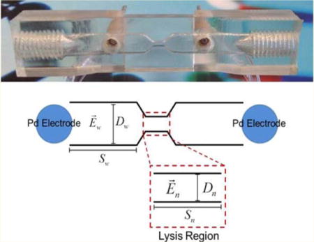
Figure 1.
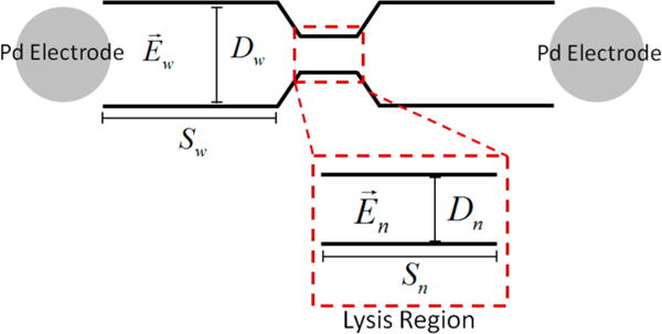
Schematic of the channel geometry used in the 3D-printed fluidic device, highlighting the desired lysis region.
Table 1.
Channel Dimensions of Devices 1 and 2
| model |
Dw (mm) |
Dn (mm) |
Sw (mm) |
Sn (mm) |
Voltage (V) |
Ew (V cm−1) |
En (V cm−1) |
|---|---|---|---|---|---|---|---|
| device 1 | 5.0 | 1 | 5 | 2 | 500 | 250 | 1250 |
| device 2 | 3.8 | 1 | 5 | 2 | 500 | 283 | 1084 |
The most common methodology for electrical lysis of cells utilizes pulsed electric field strengths ranging from one to several hundred kV cm−1 with microsecond to millisecond potential durations.30 In order for a low-voltage power supply (500 V max voltage) to be utilized, the geometry of the internal channel was augmented in areas so that an electric field greater than 1000 V cm−1 could be generated. Wang et al. and Lee et al. have shown that, for a channel with uniform depth but varying width, a higher electric field can be generated in a narrow region, and the electric fields in the wide and narrow regions can be calculated with the following equations:2,7
| (3) |
| (4) |
where represents the electric field in the wide (w) or narrow (n) region, S is the segment length, D is the diameter of the channel, and voltage is the applied potential. Two devices were fabricated to see which geometry would provide more selective lysis isolated to the tapered region of the channel. Electric fields greater than 1000 V cm−1 were calculated for the lysis region, while in the wide regions, electric fields were 250 and 283 V cm−1 for devices 1 and 2, respectively, when a 500 V potential was used for voltage. These calculated theoretical electric fields helped to guide the design of the devices and gave an indication of the potential necessary to achieve lysis. However, coating the devices with PDMS and PS changes the geometry of the channel. Therefore, these values are merely guidelines. Figure 2 shows the actual 3D-printed device complete with removable electrodes.
Figure 2.
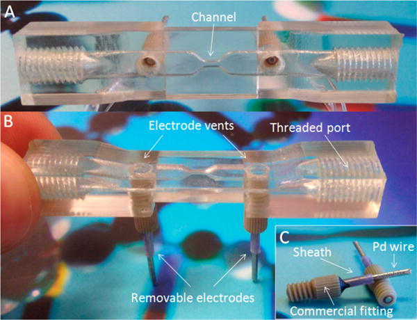
3D-printed device images. Top view of the device showing the geometry of the channel between the two electrodes (A). Side view of the device highlighting the electrode vents, removable electrodes at the base of the device, and threaded ports for sample incorporation (B). Profiles of the removable electrodes showing the 2 mm diameter palladium wire inserted into a commercial sheath that is fixed into a commercial fitting using epoxy and quick weld (C).
Optical Characterization of the Device
Employing a polyjet 3D-printed device for studies where optical measurements are desired poses a challenge due to the inability to polish internal surfaces that remain rough and opaque after clearance of support material. The printer manufacturer (Stratasys) suggests NaOH vapor as a chemical means for polishing Vero Clear, but this degrades the integrity of printed features such as threading. SEM images (Figure 3) revealed that the top and bottom of channels in the devices were smooth after printing, while the sides were rough and integrate more with support material—indicating a limitation in accuracy for this dimension. Even after removal of support material, the rough sides remain, posing a possible limitation of fabricating channels with this type of printer. For visualization purposes, it becomes necessary to orient the device during printing so that the optical path aligns with the smooth edges.
Figure 3.
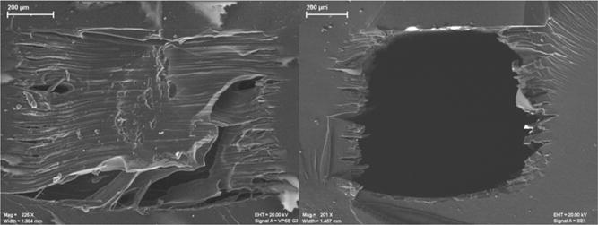
SEM images of cross sections of an untreated 1 mm × 0.8 mm channel. Cross section of a channel after printing with support material still present (left). Cross section of a channel after removal of support material (right).
A majority of 3D-printed materials are proprietary in nature. Being able to incorporate well-characterized materials will expand the utility of 3D printing beyond what is currently possible. PDMS has a refractive index (1.43) close to that of Vero Clear (1.47), limiting the effect incorporation will have on making optical measurements. Due to its viscous nature before curing, PDMS makes an ideal candidate for coating the surface of channels, making them visually clear. Furthermore, PDMS is well-established as a nontoxic, oxygen-permeable substrate onto which cells can adhere and grow.16,18 Various ratios of PDMS (5:1, 10:1, and 20:1) were tested to examine the ability to cure on a flat piece of printed Vero Clear material. Of the three ratios tested, 10:1 was the best able to cure to the printed material (fastest cure time at room temperature). We found that PDMS would not cure inside the channel of the device unless both were plasma-treated. However, concurrent exposure of 10:1 PDMS and the 3D-printed device to plasma served to oxidize the exposed surface area of the PDMS, which thickened when mixed before incorporation into the fluidic channel. In our attempts to expose just the printed device to oxygen plasma (or PDMS exclusively), we found that the PDMS did not cure as effectively. This is similar to the process of irreversibly sealing PDMS to glass, where both are exposed to plasma before adhering. While a flat piece of printed Vero Clear material (3 cm × 3 cm × 3 mm) was amenable to visualization of cell adherence and growth over a 48 h period (data not shown), the same cannot be said of cells growing within a channel of a device, making PDMS or PS coating necessary.
Uncoated Vero Clear (no treatment and polished), PDMS-coated, and PS-coated Vero Clear samples were analyzed for percent transmittance using a UV–vis spectrophotometer to determine to what extent incorporation of PDMS and PS effected optical clarity. Furthermore, a comparison of the optical clarity between matte and glossy finish for polyjet 3D-printed parts was made. Each sample prepared was 3 mm thick, and transmittance data were collected from 200 to 800 nm. Figure 4 shows the percent transmittance data for each sample. Devices printed with a glossy finish and coated with PS had the highest percent transmittance of any coated device, while polished devices with a glossy finish reported the overall highest transmittance. Future studies carrying out optical measurements on polyjet 3D-printed parts would be best suited to utilize a glossy finish.
Figure 4.
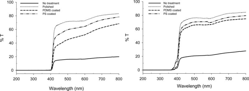
Percent transmittance of Vero Clear (no treatment and polished), PDMS-coated, and PS-coated slabs when printed in standard format (left) and printed with a glossy finish (right).
For SEM analysis, cross sections of bare channels and those coated with PS or PDMS were imaged to determine coating thickness. PDMS coating varied in thickness from about 3 μm near the bottom of the channel to over 100 μm at the sides and formed a more circular channel by integrating into the various contours along the sides of the channel, as seen in the top panel of Figure 5. The PS-coated device required multiple coatings to completely fill in the sides of the channel, and the thickness after three coatings extended beyond 100 μm in some areas (Figure 5 bottom panel).
Figure 5.
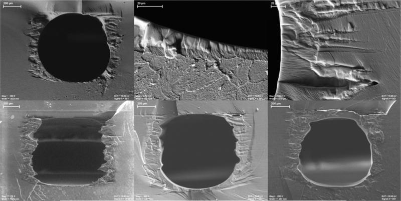
SEM images of channels coated with PDMS (top panel) or PS (bottom panel). Top panel: PDMS-coated channel (left), contrast between Vero Clear printed material and PDMS coating at the bottom of the channel (center), and PMDS integrating into printed contours (right). Bottom panel: Channel coated with one layer of PS (left), two layers of PS (center), and three layers of PS (right).
Lysis of Adhered Endothelial Cells
Prior to lysis, cell viability on the device was evaluated. After 5 days, 94% of the cells remaining on the device were viable, as confirmed by live and dead cell stains. However, there was an overall decrease in cell coverage on the device after day 4 (Figure S2).
Lower end potentials (device 1, 50 and 75 V; device 2, 100 and 125 V) led to incomplete lysis, as evidenced by the presence of cells in the lysis region, while higher end potentials (device 1, 125 and 150 V; device 2, 175 and 200 V) led to lysis that was not confined to the desired lysis region. However, for both geometries, an optimal potential (device 1, 100 V; device 2, 150 V) was found that allowed for selective lysis in the desired region while maintaining cell integrity in the surrounding areas. Figure 6A,B shows the cell lysis efficiencies represented as percent cell lysis for devices 1 and 2, respectively. For device 1, the following are the calculated electric fields in the lysis region according to eq 4 and the corresponding applied potentials: 50 V (125 V cm−1), 75 V (187.5 V cm−1), 100 V (250 V cm−1), 125 V (312.5 V cm−1), and 150 V (375 V cm−1). For device 2, these values are 100 V (217 V cm−1), 125 V (271 V cm−1), 150 V (325 V cm−1), 175 V (380 V cm−1), and 200 V (434 V cm−1). The lower end applied potentials resulted in more variable cell lysis efficiencies, which can be attributed to the reduced electric fields that cells experience at these potentials.
Figure 6.
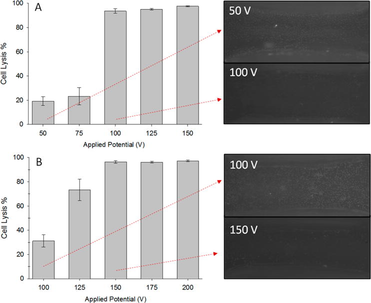
Cell lysis efficiencies for devices 1 and 2 with corresponding images of cells remaining on the device from the tapered region when insufficient (50 and 100 V) and optimal (100 and 150 V) potentials were applied. Device 1: Potentials ranged from 50 to 150 V. Incomplete lysis was seen with applied potentials of 50 and 75 V, while nearly complete clearance of cells was seen for 100–150 V: 50 V (potential duration 4 ± 1 s, n = 10), 75 V (3.5 ± 1 s, n = 8), 100 V (3 ± 1 s, n = 9), 125 V (2 ± 1 s, n = 6), 150 V (2 ± 1 s, n = 6). Cell lysis efficiency error: S.E.M., potential duration: Stdev. (A). Device 2: Applied potentials ranged from 100 to 200 V. Incomplete lysis was seen with applied potentials of 100 and 125 V, while nearly complete clearance of cells was seen for 175–200 V: 100 V (potential duration 3 ± 1 s, n = 7), 125 V (3 ± 1 s, n = 9), 150 V (2.5 ± 1 s, n = 6), 175 V (2 ± 0.5 s, n = 5), 200 V (2 ± 1 s, n = 6). Cell lysis efficiency error: S.E.M., potential duration: Stdev. (B).
The electric fields that cells were exposed to in this study did not reach the calculated theoretical value needed for cell lysis (1000 V cm−1). One explanation for why much lower electric fields led to cell lysis could be due to PDMS incorporation decreasing the true geometry of the internal channel and skewing the calculated electric fields. Furthermore, accounts of lower electric fields (<1000 V cm−1) leading to cell lysis with extended field duration (millisecond) or decreased distance between electrodes have been reported.3,14,15 The PDMS-coated device that was interfaced with removable electrodes that were used in this study exhibited area-specific electrical cell lysis.
A thermocouple was used to determine the temperature change that occurred when using the optimal potentials for both models over a 5 s application in both wide and narrow sections. Thermocouple measurements were made on the outside of the device, directly over either the wide or narrow regions. The distance between the channel and outside of the device in each case was a couple of millimeters. For both models, no significant change in temperature occurred in the wide sections. For device 1, there was a 2 °C increase in the middle section, and no change in the middle section of device 2. The current generated during cell lysis generally ranged from 1 to 8 mA for device 1 and from 8 to 20 mA for device 2. Generation of hydroxide from the electrolysis of water has previously been used to lyse cells on microfluidic platforms31,32 though was ruled out as the lysis source here as cells remained viable outside the lysis region, as confirmed by microscopy.
CONCLUSIONS
While both PDMS and PS are amenable to cell adhesion and growth, we found that cells were better able to adhere and survive on PDMS-coated devices. For these reasons, characterization experiments were carried out with PDMS-coated devices. While there have been numerous examples demonstrating the utility of 3D-printed devices for a number of differing applications,21,33 including 3D-printed templates used for replicate molding of PDMS devices34 and transparent 3D-printed devices capable of microscope readout of dyes,35 the work presented here is the first case of immobilization of cells on 3D-printed devices featuring surface modifications with PDMS or PS. Specifically, the devices used in this study were extremely rugged, allowed for integration with commercial fittings, and were reusable over a 9 month period (and counting), therefore offering a significant advancement compared to their soft-lithography-fabricated PDMS predecessors. Currently, this protocol is being applied toward the development of a vascular injury mimic and offers more realistic in vivo conditions by omitting the addition of non-native circulation components to lyse cells. This methodology can also be applied to studies striving to dictate cell patterning within a 3D-printed device, to carry out in vitro experiments involving live cells on platforms not inherently cell-amenable, or to provide a well-characterized surface material for non-cell-based studies (electrophoresis, etc.). While the channel dimensions reported here are on a millimeter scale, the Objet Connex350 3D printer used in this study has a Z resolution (height of each layer) of 16 μm, an X/Y resolution of 100 μm, and an accuracy of 20–85 μm for features below 50 mm. Our group has found that removal of support material in channels less than 250 μm in diameter is often incomplete, limiting channel features with this type of printer. Through repeated coatings of PDMS or PS, current limitations associated with 3D printer resolution or support material removal could be avoided and channels of sub-100 μm diameter could plausibly be fabricated.
Supplementary Material
Acknowledgments
The authors thank Brian Wright from the Department of Electrical and Computer Engineering at Michigan State University for his assistance printing the devices used, and Per Askeland from the College of Engineering for his expertise in acquiring SEM images. This work was funded by NIH (Grant Nos. 1R21EB016379 and 1R01GM110406).
Footnotes
Supporting Information
Additional information as noted in text. The Supporting Information is available free of charge on the ACS Publications website at DOI: 10.1021/acs.analchem.5b01202.
Notes
The authors declare no competing financial interest.
References
- 1.Lu H, Schmidt MA, Jensen KF. Lab Chip. 2005;5:23–29. doi: 10.1039/b406205a. [DOI] [PubMed] [Google Scholar]
- 2.Wang H, Bhunia AK, Lu C. Biosens Bioelectron. 2006;22:582–588. doi: 10.1016/j.bios.2006.01.032. [DOI] [PubMed] [Google Scholar]
- 3.Lee S, Tai Y. Sens Actuators, A. 1999;73:74–79. [Google Scholar]
- 4.Di Carlo D, Jeong K, Lee LP. Lab Chip. 2003;3:287–291. doi: 10.1039/b305162e. [DOI] [PubMed] [Google Scholar]
- 5.Irimia D, Tompkins RG, Toner M. Anal Chem. 2004;76:6137–6143. doi: 10.1021/ac0497508. [DOI] [PubMed] [Google Scholar]
- 6.Waters LC, Jacobson SC, Kroutchinina N, Khandurina J, Foote RS, Ramsey MJ. Anal Chem. 1998;70:158–162. doi: 10.1021/ac970642d. [DOI] [PubMed] [Google Scholar]
- 7.Lee DW, Cho Y. Sens Actuators, B. 2007;124:84–89. [Google Scholar]
- 8.Huang Y, Mather EL, Bell JL, Madou M. Anal Bioanal Chem. 2002;372:49–65. doi: 10.1007/s00216-001-1191-9. [DOI] [PubMed] [Google Scholar]
- 9.Ward M, Wu J, Chiu J. J Acoust Soc Am. 1999;105:2951–2957. doi: 10.1121/1.426908. [DOI] [PubMed] [Google Scholar]
- 10.Sims CE, Meredith GD, Krasieva TB, Berns MW, Tromberg BJ, Allbritton NL. Anal Chem. 1998;70:4570–4577. doi: 10.1021/ac9802269. [DOI] [PubMed] [Google Scholar]
- 11.Kim J, Jang SH, Jia G, Zoval JV, Da Silva NA, Madou MJ. Lab Chip. 2004;4:516–522. doi: 10.1039/b401106f. [DOI] [PubMed] [Google Scholar]
- 12.Kim YC, Kang JH, Park SJ, Yoon ES, Park JK. Sens Actuators, B. 2007;128:108–116. [Google Scholar]
- 13.Schilling EA, Kamholz AE, Yager P. Anal Chem. 2002;74:1798–1804. doi: 10.1021/ac015640e. [DOI] [PubMed] [Google Scholar]
- 14.McClain MA, Culbertson CT, Jacobson SC, Albritton NL, Sims CE, Ramsey MJ. Anal Chem. 2003;75:5646–5655. doi: 10.1021/ac0346510. [DOI] [PubMed] [Google Scholar]
- 15.Wang H, Lu C. Anal Chem. 2006;78:5158–5164. doi: 10.1021/ac060733n. [DOI] [PubMed] [Google Scholar]
- 16.Chiu DT, Jeon NL, Huang S, Kane RS, Wargo CJ, Choi IS, Ingber DE, Whitesides GM. Proc Natl Acad Sci USA. 2000;97:2408–2413. doi: 10.1073/pnas.040562297. [DOI] [PMC free article] [PubMed] [Google Scholar]
- 17.van der Meer AD, Poot AA, Duits MHG, Feijen J, Vermes I. J Biomed Biotechnol. 2009;2009:823148. doi: 10.1155/2009/823148. [DOI] [PMC free article] [PubMed] [Google Scholar]
- 18.McDonald JC, Whitesides GM. Acc Chem Res. 2002;35:491–499. doi: 10.1021/ar010110q. [DOI] [PubMed] [Google Scholar]
- 19.Johnson AS, Anderson KB, Halpin ST, Kirkpatrick DC, Spence DM, Martin RS. Analyst. 2013;138:129–136. doi: 10.1039/c2an36168j. [DOI] [PMC free article] [PubMed] [Google Scholar]
- 20.Stjernstrom M, Roeraade JJ. Micromech Microeng. 1998;8:33–38. [Google Scholar]
- 21.Gross BC, Erkal JL, Lockwood SY, Chen C, Spence DM. Anal Chem. 2014;86:3240–3253. doi: 10.1021/ac403397r. [DOI] [PubMed] [Google Scholar]
- 22.Seitz H, Rieder W, Irsen S, Leukers B, Tille C. J Biomed Mater Res Part B. 2005;74B:782–788. doi: 10.1002/jbm.b.30291. [DOI] [PubMed] [Google Scholar]
- 23.Mironov V, Boland T, Trusk T, Forgacs G, Markwald RR. Trends Biotechnol. 2003;21:157–161. doi: 10.1016/S0167-7799(03)00033-7. [DOI] [PubMed] [Google Scholar]
- 24.Landers R, Hubner U, Schmelzeisen R, Mulhaupt R. Biomaterials. 2002;23:4437–4447. doi: 10.1016/s0142-9612(02)00139-4. [DOI] [PubMed] [Google Scholar]
- 25.Leclerc E, Sakai Y, Fujii T. Biomed Microdevices. 2003;5:109–114. [Google Scholar]
- 26.Curtis AS, Forrester JV, McInnes C, Lawrie F. J Cell Biol. 1983;97:1500–1506. doi: 10.1083/jcb.97.5.1500. [DOI] [PMC free article] [PubMed] [Google Scholar]
- 27.Wang Y, Balowski J, Phillips C, Phillips R, Sims CE, Allbritton NL. Lab Chip. 2011;11:3089–3097. doi: 10.1039/c1lc20281b. [DOI] [PMC free article] [PubMed] [Google Scholar]
- 28.Willis K, Brockmeyer E, Hudson S, Poupyrev I. Proceedings of the 25th Annual ACM Symposium on User Interface Software and Technology. ACM; New York: 2012. 3D printing of embedded optical elements for interactive devices; pp. 589–598. [Google Scholar]
- 29.Zimmermann U. Trends Biotechnol. 1983;1:149–155. [Google Scholar]
- 30.Morshed BI, Shams M, Mussivand T. Crit Rev Biomed Eng. 2013;41:37–50. doi: 10.1615/critrevbiomedeng.2013006378. [DOI] [PubMed] [Google Scholar]
- 31.Di Carlo D, Ionescu-Zanetti C, Zhang Y, Hung P, Lee LP. Lab Chip. 2005;5:171–178. doi: 10.1039/b413139h. [DOI] [PubMed] [Google Scholar]
- 32.Nevill JT, Cooper R, Dueck M, Breslauer DN, Lee LP. Lab Chip. 2007;7:1689–1695. doi: 10.1039/b711874k. [DOI] [PubMed] [Google Scholar]
- 33.Kitson PJ, Rosnes MH, Sans V, Dragone V, Cronin L. Lab Chip. 2012;12:3267–3271. doi: 10.1039/c2lc40761b. [DOI] [PubMed] [Google Scholar]
- 34.Comina G, Suska A, Filippini D. Lab Chip. 2014;14:424–430. doi: 10.1039/c3lc50956g. [DOI] [PubMed] [Google Scholar]
- 35.Shallan AI, Smejkal P, Corban M, Guijt RM, Breadmore MC. Anal Chem. 2014;86:3124–3130. doi: 10.1021/ac4041857. [DOI] [PubMed] [Google Scholar]
Associated Data
This section collects any data citations, data availability statements, or supplementary materials included in this article.