Abstract
Commercially available near-infrared (IR) imagers are fabricated by integrating expensive epitaxial grown III-V compound semiconductor sensors with Si-based readout integrated circuits (ROIC) by indium bump bonding which significantly increases the fabrication costs of these image sensors. Furthermore, these typical III-V compound semiconductors are not sensitive to the visible region and thus cannot be used for multi-spectral (visible to near-IR) sensing. Here, a low cost infrared (IR) imaging camera is demonstrated with a commercially available digital single-lens reflex (DSLR) camera and an IR sensitive organic light emitting diode (IR-OLED). With an IR-OLED, IR images at a wavelength of 1.2 µm are directly converted to visible images which are then recorded in a Si-CMOS DSLR camera. This multi-spectral imaging system is capable of capturing images at wavelengths in the near-infrared as well as visible regions.
Near infrared (NIR) imaging devices have attracted a great deal of research interest because of their potential applications in range finding, security, semiconductor wafer inspections as well as medical imaging1,2,3,4. The spectral region between 1 and 1.8 µm is of particular commercial interest due to the low water absorption in this range. Currently, commercial NIR imagers are fabricated by integrating III-V compound semiconductor sensors with Si-based readout integrated circuits (ROIC) by indium bump bonding. There are two problems with these devices. First, because of the high density interconnects required for imaging, the photodetector-ROIC bonding process dramatically increases the fabrication costs and severely limits the applications of these image sensors. Second, one would like to have an imaging system which can detect NIR as well as visible images. However, typical III-V compound semiconductors sensitive to the NIR region such as InGaAs are not sensitive to the visible region and they cannot be used for sensing in the visible region.
Optical up-conversion devices, capable of producing pixelless images, have been demonstrated in the last two decades as an alternative technology for infrared (IR) imaging5,6,7. Up-conversion devices based on inorganic compound semiconductors have been fabricated by integrating an IR photodetector with a light emitting diode (LED). However, growing an inorganic LED on top of a photodetector requires lattice matching of two material systems; as a result, only a limited choice of materials are available. For example, III-V semiconductor based up-conversion devices can only up-convert light of wavelength 1.5 µm to 1 µm, and the final NIR image is captured using a conventional silicon CCD camera8,9. For IR-to-visible up-conversion, IR-to-visible up-conversion devices have been demonstrated by integrating an InGaAs/InP photodetector with an organic light emitting diode (OLED)10,11,12,13. However, these up-conversion devices still require epitaxially growth of inorganic semiconductor materials which are expensive to synthesize.
In order to realize low cost pixelless IR imaging, we recently demonstrated IR sensitive organic LEDs (IR-OLEDs) which have a similar structure compared with conventional OLEDs. The IR-OLED functions as an IR-to-visible up-conversion device with an IR sensitizer which can either be a thermally evaporated organic semiconductor or a solution processed colloidal inorganic semiconductor nanocrystals (NCs)14,15 thin film. Using SnPc:C60 as the sensitizer, we have demonstrated IR-OLEDs sensitive up to 900 nm. Using solution processed colloidal PbSe NCs as the IR sensitizer, these IR-OLEDs show an IR sensitivity up to 1.5 µm. In this work, by incorporating a transparent IR-OLED in a commercial digital single-lens reflex (DSLR) camera, a multi-spectral imaging system capable of NIR as well as visible imaging is realized. A schematic diagram of the imaging system is shown in Figure 1a.
Figure 1. Schematic illustration of the multi-spectral imaging camera.
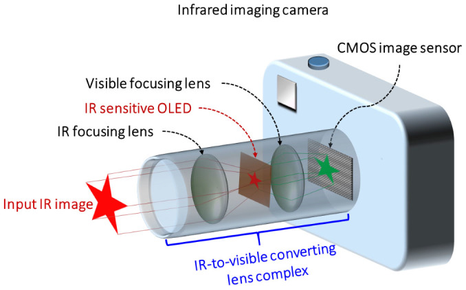
Schematic diagram of the infrared imaging camera with a commercial DSLR camera and an IR-OLED.
Results
Fabrication of transparent IR sensitive OLED
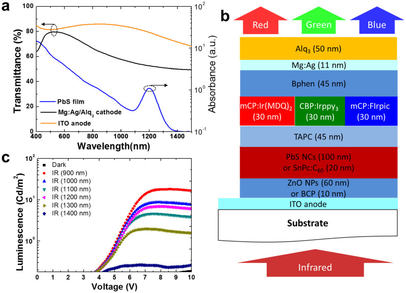
To demonstrate direct IR imaging, transparent IR-OLEDs are first fabricated with an ITO bottom anode and a semi-transparent top cathode. Previously, we reported IR-OLEDs with a top reflective Al cathode. To fabricate transparent IR-OLEDs, a semi-transparent top cathode consists of a 11 nm-thick Mg:Ag (10:1 ratio) film and a 50 nm-thick tris(8-hydroxyquinolinato) aluminum (Alq3) film. The Alq3 film maximizes the optical transparency of the top electrode stack as an index-matching layer in the transparent device. The Mg:Ag/Alq3 top electrode stack shows a transparency of 79% at 515 nm as shown in Figure 2a. To evaluate the optical transparency of the Mg:Ag/Alq3 stack in an OLED, we fabricated transparent OLEDs with this semi-transparent top electrode. As expected, light emitted from the transparent OLED exits to both sides of the device. Figures S1 (a) and (b) show 40% of the emitted green light exits through the top electrode and 60% of the light exits through the bottom electrode. Because the ITO anode has a higher optical transparency than the Mg:Ag/Alq3 electrode as shown in Figure 2a, the light output through the bottom ITO electrode is slightly higher than that through the top electrode.
Figure 2. Transparent infrared sensitive OLED.
(a) The absorbance spectrum of the PbS NCs IR sensitizing layer, and the transparency spectra of the ITO bottom and the Mg:Ag/Alq3 top cathode. (b) Schematic cross section view of the transparent IR-OLEDs with the ITO bottom electrode, and the Mg:Ag/Alq3 top electrode. (c) L-V characteristics of the IR-OLED with a PbS IR sensitizer in the dark and under different IR illuminations.
A schematic cross section view of a transparent IR-OLED is shown in Figure 2b. The device is basically an OLED with an IR sensitizing layer. The key to IR-OLEDs is to keep the device in an off-state even if a forward voltage is applied to the device, and turn on the device only with infrared light. To keep the device off under forward bias, a hole blocking layer (HBL) is inserted between the ITO anode and the IR sensitizer to block hole injection from the anode15. Under IR irradiation, photo-generated holes in the IR sensitizing layer are injected through the hole transport layer (HTL) into the emitting layer of the OLED and recombine with electrons injected from the cathode to emit visible light. (Supplementary Figure S2) Complete fabrication details of the transparent IR-OLEDs are described in the Method section.
Figure 2c shows the luminance-voltage (L-V) characteristics of the transparent IR-OLEDs with an ITO bottom electrode and a semi-transparent Mg:Ag/Alq3 top electrode in the dark and different IR wavelengths (900 nm, 1000 nm, 1100 nm, 1200 nm, 1300 nm, 1400 nm). Without IR excitation, there is no light emission at voltages up to 10 V, indicating that the ZnO NPs HBL blocks hole injection from the ITO anode effectively. Upon excitation with IR light from the ITO bottom electrode, the device current turns on at about 4 V along with an onset of green light emission through the top electrode. The luminance in the device increases with increasing voltage, saturating at voltages beyond 6 V. The transparent IR-OLED with a PbS IR sensitizing layer responds to IR irradiation with wavelength up to 1400 nm.
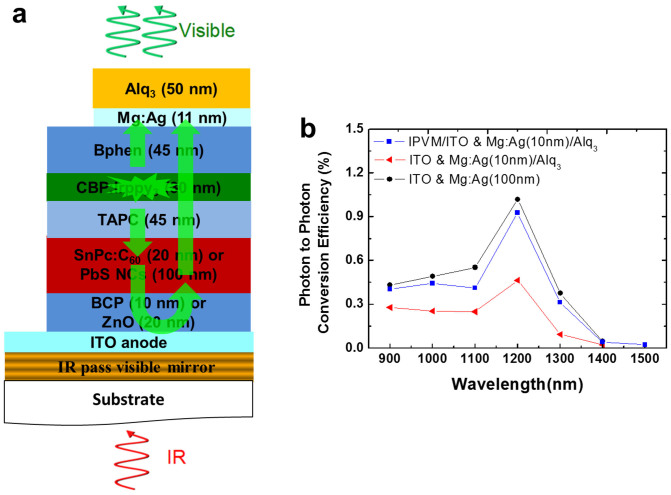
To further enhance the optical performance of the device, an IR-pass-visible-mirror (IPVM), which transmits IR and reflects visible light, is inserted between the glass substrate and the ITO anode. Specifically, this IPVM allows transmission of the incident infrared light through the bottom electrode but reflects the emitted visible light from the OLED, and the light output through the top electrode in the resulting transparent IR-OLED is enhanced as shown in Figure 3a. The IPVM used in our devices, consisting of 22 layers of alternating low-index (SiO2)/high-index (TiO2) dielectric thin films, is a dichroic mirror which reflects only visible light of wavelengths from 400 nm to 650 nm, but transmits IR light. The ITO/IPVM coated substrate shows a high transparency in the IR range (92% transparency at 740 nm and 81% transparency at 1200 nm) and a high reflectivity in the visible range (99.53% reflectivity at 515 nm) as shown in Supplementary Figure S3 (a). To evaluate the optical effect of the IPVM stack, we also fabricated a top emitting OLED on an IPVM coated substrate with a semi-transparent Mg:Ag/Alq3 top electrode. 97% of the emitted light exited through the top electrode, indicating that the IPVM stack reflects visible light effectively. (Figures S3 (b) and (c)).
Figure 3. Effect of IPVM on IR sensitive OLED.
(a) Schematic cross section view of a top emitting IR-OLEDs with an IPVM/ITO bottom electrode and a Mg:Ag/Alq3 top electrode. (b) Photon (IR)-to-photon (Visible) conversion efficiency spectra of the reflective, transparent, and top emitting IR-OLEDs.
Figure 3b shows the spectral photon-to-photon (P-P) conversion efficiencies of reflective (ITO anode and Al cathode), transparent (ITO anode and Mg:Ag cathode), and top emitting (IPVM/ITO anode and Mg:Ag cathode) IR-OLEDs with a PbS NCs IR sensitizing layer. The P-P conversion efficiency spectra are similar to the absorption spectrum of the PbS NCs film. The peak wavelength in the conversion efficiency spectra is 1200 nm and the maximum P-P conversion efficiency at the peak wavelength at 10 V is 1.02%, 0.46%, and 0.93% for the reflective, transparent, and top emitting devices, respectively. Compared to the transparent device, the top emitting device with an IPVM has a 2-fold enhancement in conversion efficiency and its P-P conversion efficiency is almost the same as that of the reflective device, indicating that the IPVM stack reflects the emitted visible light effectively. The spectral p-p conversion efficiencies in the IR-OLEDs with an organic IR sensitizing layer are also shown in the Supplementary Section. The peak wavelength in the P-P conversion efficiency spectra is 740 nm and the maximum P-P conversion efficiencies at the peak wavelength of 740 nm at 12 V are 11.3%, 5.1%, and 10.5% in the reflective, transparent, and top emitting devices, respectively. (Supplementary Figure S4).
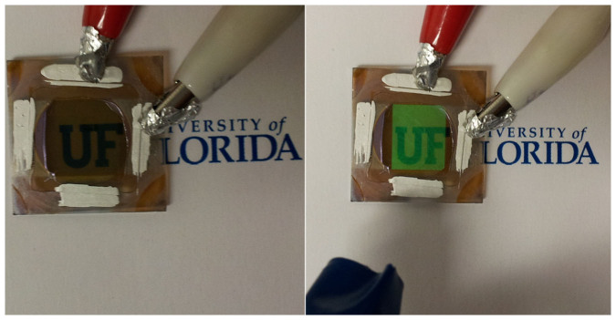
Figure 4 shows the images of the transparent IR sensitive OLED with the PbS IR sensitizing layer at 10 V with and without 1.2 µm IR illumination. The transparent device comprising 8 organic and inorganic layers, a glass substrate, and an encapsulation cap glass shows a transparency of 40% in the visible range. This transparency provides an opportunity to employ this device for direct imaging in both NIR and visible regions which we will present in the next section. Flexible IR-OLEDs with the organic IR sensitizer have also been fabricated on PET substrates. A glass substrate was used as a rigid sample carrier for all processes including the vacuum evaporation by attaching the plastic substrate with double sided tapes. The p-p conversion efficiencies of the flexible IR-OLEDs at the peak wavelength of 740 nm are 4.1% and 1.1% for the reflective and transparent devices, respectively and the device in operation is also shown in Figure S5.
Figure 4. Images of transparent IR sensitive OLED.
Images of a transparent IR-OLED with a PbS IR sensitizer operated in ambient light (left) and under IR illumination (right).
Demonstration of multi-spectral imaging
In order to demonstrate the IR imaging capability, we first fabricated a monocular direct view IR imager with the transparent IR sensitive OLED as shown in the Figure S6. The optics of the monocular direct view prototype has an objective lens with a focal length of 25 mm and an aperture of f/1.4. The active device area is 1 cm2. This device has only one anode pad and one cathode pad for supplying the electrical power. An IR flash light was made with an array of 1.2 µm IR LEDs. The photo images of “UF” were taken in ambient lighting conditions and in the dark illuminated with the IR flash light as shown in Figure 5. The up-converted visible images were clear, indicating the high quality pixelless imaging capability of IR-OLEDs. In a typical inorganic up-conversion device using III-V compound semiconductors, it is challenging to have sharp up-conversion images due to the lateral carrier diffusion in the electrical interconnecting unit between the photodetector and LED13. On the other hand, in our IR-OLEDs made with thin films, holes generated in the IR sensitizer are injected to the emitting layer through the organic hole transport layer. Because the layers between the two electrodes have a poor conductivity, lateral diffusion of carriers is suppressed. As a result, the upper limit of the image resolution in our IR-OLED should be the sum of the film thicknesses [(PbS NCs (100 nm), TAPC (40 nm), CBP:Irppy3 (30 nm), BPhen (40 nm))] which is about 220 nm. Thus, high quality up-converted images can be realized in the IR-OLED as shown in Figure 5.
Figure 5. Demonstration of pixelless IR imaging.
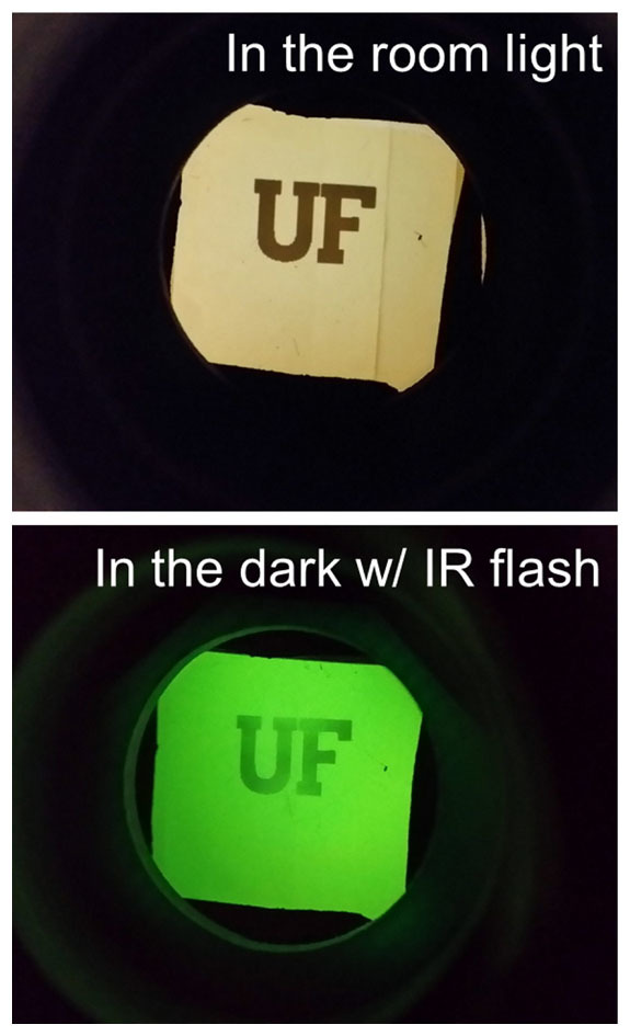
The photo images of the pixelless IR imaging demonstration by a monocular direct view IR imager fabricated with a transparent IR sensitive OLED under room light (top) and in the dark with the 1.2 µm IR flash light (bottom).
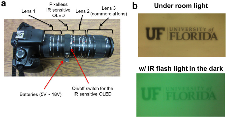
Figure 6a shows an IR imaging camera integrating an IR-to-visible converting lens system with a commercial DSLR camera. The optics of the IR-to-visible converting lens system, which is similar to the direct view IR monocular imager, consists of three lenses. Lens 1 and Lens 2 are the chromatic doublet lenses used to minimize spherical aberration and Lens 3 is the objective lens from the DSLR camera. The achromatic doublet lens consists of two lenses with different amounts of dispersion. One element is a negative (concave) element which has relatively high dispersion and the other is a positive (convex) element which has a lower dispersion so that the chromatic aberration of one is counterbalanced by the other. The infrared image focused on the transparent IR-OLED by Lens 2 is converted to a visible image, which is then focused on the CMOS image sensor by Lens 1. The resulting image was recorded in a digital image format. For camera applications, we also used an IR-OLED with an active area of 1 cm2. The photo images of “University of Florida” were taken in ambient light and in the dark with the 1.2 μm IR flash light as shown in Figure 6b. It should be noted that the DSLR camera with an IR-OLED not only functions as an IR imaging device but also a normal visible imaging device. Therefore, a low cost multi-spectral (visible to NIR) imaging device using a commercially available DSLR camera is realized.
Figure 6. Multi-spectral imaging camera.
(a) Image of the multi-spectral imaging camera by incorporating an IR-OLED in a commercially available DSLR camera. This is done by inserting a transparent IR-OLED between two achromatic doublet lenses in the DSLR camera. (b) Images taken by the multi-spectral imaging camera under the room light (top) and in the dark with IR flash (bottom).
Discussion
For optimum optical design, custom optics should be used to produce a more compact optical system. We estimate the cost of such a system will be comparable to the cost of currently available optics used for consumer cameras. Thus, low cost, high quality IR imaging systems can be realized. These devices can be incorporated into consumer cameras with minimal additional costs. As shown in Figure S7, PbS NCs can be sensitive to wavelengths beyond 2 μm, it is expected that this multi-spectral imaging device can be useful for imaging from 400 nm to 2 μm.
In conclusion, we have demonstrated a low cost multi-spectral camera by incorporating an IR-OLED in a commercially available DSLR camera. This is done by inserting a transparent IR-OLED between two achromatic doublet lenses in the DSLR camera. IR images of 1.2 µm wavelength are converted directly to visible images with a resolution less than a micron. The IR-OLEDs have a similar structure with a manufacturing process similar to conventional OLEDs for display and lighting applications. Flexible IR-OLEDs have also been demonstrated, and compact imaging systems can be realized with these devices.
Methods
Synthesis of colloidal nanocrystals (ZnO, PbS)
ZnO NCs were synthesized by a sol-gel process using precursors of zinc acetate and tetramethylammonium hydroxide (TMAH). PbS NCs were synthesized by decomposition of organometallic precursors as reported previously and washed by precipitation and re-dispersion three times. Subsequently, the original long-chain oleate ligands on the nanocrystal surface were exchanged with octylamine, which is a shorter capping group. The surface-exchanged nanocrystals were washed and redispersed in chloroform. The nanocrystals solutions were filtered using a 0.45 µm filter.
Device fabrication
IR-OLEDs were fabricated on patterned ITO substrates with a sheet resistance of 20 Ω per square. The substrates were first cleaned with acetone and isopropanol in an ultrasonic cleaner and subsequently rinsed with de-ionized water, blown dry with N2 gas, and treated with UV ozone. For IR-OLEDs with a colloidal PbS nanocrystals (NCs) IR sensitizer, a 60 nm layer of ZnO nanoparticles was spin-coated on top of the ITO substrate and then annealed at 90°C for 15 minutes in the ambient. The substrate was subsequently introduced into a nitrogen glove box and a 100 nm PbS NCs layer was spin-coated. The PbS nanocrystal layer was then treated with a benzenedithiol (BDT) solution to improve electronic coupling between individual NCs. For IR-OLEDs with an organic tin phthalocyanine (SnPc):C60 IR sensitizer, a 10 nm layer of bathocuproine (BCP) was deposited on the top of the ITO substrate as a hole blocking layer (HBL) by thermal evaporation. A SnPc:C60 mixed layer was deposited on the hole blocking layer as a NIR-sensitizing layer. SnPc and C60 were purified three times by train sublimation technique16. After depositing the HBL and the IR sensitizing layer, an OLED is fabricated on top, and it has the following structure: a 45 nm-thick 1,1-bis[(di-4-tolylamino) phenyl]cyclohexane (TAPC) layer was used as a hole transporting material, a 30 nm-thick 4,4-N,Ndicarbazole-biphenyl (CBP) layer doped with fac-tris(2-phenylpyridinato)iridium(III) (Irppy3) was used as an green emitting layer, a 30 nm-thick N,N′-dicarbazolyl-3,5-benzene (mCP) layer doped with iridium(III)bis(2-methyldibenzo[f,h]quinoxaline) (acetylacetonate) (Ir(MDQ)2) was used as an red emitting layer, a 30 nm-thick N,N′-dicarbazolyl-3,5-benzene (mCP) layer doped with bis[(4,6-di-fluorophenyl)-pyridinate-N,C2′]picolinate (FIrpic) was used as an blue emitting layer, and 4,7-diphenyl-1,10-phenanthroline (BPhen) (45 nm) was used as a hole blocker/electron transporting layer (ETL). Mg:Ag films (10:1 ratios) of 100 nm and of 11 nm were used as the cathode for reflective device and transparent devices, respectively. All layers in the IR sensitive OLED were vacuum deposited at a pressure of 1 × 10⁻⁶ Torr. The areas of the device are 0.04 cm2 and 1 cm2.
Device characterization
Luminance-current-voltage (LIV) characteristics of the IR sensitive OLED devices were measured using a Keithley 4200 semiconductor characterization system connected to a calibrated Si photodiode for photocurrent measurements. A 150 W ozone free xenon arc lamp coupled with a monochromator was used as an IR light source to produce a monochromatic light for device characterization. The devices were encapsulated and the measurements were carried out at room temperature under ambient atmosphere.
Supplementary Material
Supplementary informaton
Acknowledgments
The authors thank Mark Davidson (University of Florida) for technical support. The authors gratefully acknowledge financial support for the research from Nannoholdings LLC. The University of Florida has filed patent applications for the infrared sensitive OLED architecture and for its use in infrared imaging applications.
Footnotes
The authors declare no competing financial interests.
Author Contributions D.Y.K. conceived the idea of multi-spectral imaging prototype, and performed IR sensitive OLED fabrication, characterization and data analysis. T.-H.L. performed transparent IR sensitive OLED fabrication, characterization and data analysis. J.W.L. performed PbS nanocrystals synthesis. J.R.M. performed ZnO nanoparticles synthesis. F.S. initiated and supervised the project. All authors discussed the results and commented on the manuscript.
References
- Kallhammer J. E. Imaging: The road ahead for car night-vision. Nature Photon. 5, 12–13 (2006). [Google Scholar]
- Welsher K. et al. A route to brightly fluorescent carbon nanotubes for near-infrared imaging in mice. Nature Nano. 4, 773–780 (2009). [DOI] [PMC free article] [PubMed] [Google Scholar]
- Gao X. H., Cui Y. Y., Levenson R. M., Chung L. W. K. & Nie S. M. In vivo cancer targeting and imaging with semiconductor quantum dots. Nature Biotechnol. 22, 969–976 (2004). [DOI] [PubMed] [Google Scholar]
- Barton J. B., Cannata R. F. & Petronio S. M. InGaAs NIR focal plane arrays for imaging and DWDM applications. Pro. SPIE 4721, 37–47 (2002). [Google Scholar]
- Liu H. C., Li J., Wasilewski Z. R. & Buchanan M. Integrated quantum well intersub-band photodetector and light emitting diode. Electron. Lett. 31, 832–833 (1995). [Google Scholar]
- Liu H. C., Allard L. B., Buchanan M. & Wasilewski Z. R. Pixelless infrared imaging device. Electron. Lett. 33, 379–380 (1997). [Google Scholar]
- Liu H. C., Gao M. & Poole P. J. 1.5 µm up-conversion device. Electron. Lett. 36, 1300–1301 (2000). [Google Scholar]
- Dupont E. et al. Pixelless thermal imaging with integrated quantum-well infrared photodetector and light-emitting diode. IEEE Photon. Technol. Lett. 14, 182–184 (2002). [Google Scholar]
- Luo H., Ban D., Liu H. C., Poole P. J. & Buchanan M. Pixelless imaging device using optical up-converter. IEEE electron device Lett. 25, 129–131 (2004). [Google Scholar]
- Ban D. et al. Near-infrared to visible light optical upconversion by direct tandem integration of organic light-emitting diode and inorganic photodetector. Appl. Phys. Lett. 90, 093108 (2007). [Google Scholar]
- Chen J. et al. Enhanced efficiency in near-infrared inorganic/organic hybrid optical upconverter with an embedded mirror. J. Appl. Phys. 103, 103112 (2008). [Google Scholar]
- Chen J., Ban D., Helander M. G., Lu Z. & Poole P. Near-infrared inorganic/organic optical upconverter with an external power efficiency of >100%. Adv. Mater. 22, 4900–4904 (2010). [DOI] [PubMed] [Google Scholar]
- Chen J. et al. Hybrid organic/inorganic optical up-converter for pixel-less near-infrared imaging. Adv. Mater. 24, 3138–3142 (2012). [DOI] [PubMed] [Google Scholar]
- Kim D. Y., Song D. W., Chopra N., Somer P. D. & So F. Organic infrared upconversion device. Adv. Mater. 22, 2260–2263 (2010). [DOI] [PubMed] [Google Scholar]
- Kim D. Y. et al. PbSe nanocrystal-based infrared-to-visible up-conversion device. Nano Lett. 11, 2109–2113 (2011). [DOI] [PubMed] [Google Scholar]
- Laudise R. A., Kloc C., Simpkins P. G. & Siegrist T. Physical vapor growth of organic semiconductors. J. Cryst. Growth 187, 449–454 (1998). [Google Scholar]
Associated Data
This section collects any data citations, data availability statements, or supplementary materials included in this article.
Supplementary Materials
Supplementary informaton


