Abstract
Microelectrode arrays offer the potential to electrochemically monitor concentrations of molecules at high spatial resolution. However, current systems are limited in the number of sensor sites, signal resolution, and throughput. Here, we present a fully integrated complementary metal oxide semiconductor (CMOS) system with an array of 32 × 32 working electrodes to perform electrochemical measurements like amperometry and voltammetry. The array consists of platinum electrodes with a center-to-center distance of 100 μm and electrode diameters of 5 to 50 μm. Currents in the range from 10 μA down to pA can be measured. The current is digitized by sigma-delta converters at a maximum resolution of 13.3 bits. The integrated noise is 220 fA for a bandwidth of 100 Hz, allowing for detection of pA currents. Currents can be continuously acquired at up to 1 kHz bandwidth, or the whole array can be read out rapidly at a frame rate of up to 90 Hz. The results of the electrical characterization meet the requirements of a wide range of electrochemical methods including cyclic voltammograms and amperometric images of high spatial and temporal resolution.
Electrochemistry offers methods to detect and monitor concentration variations of a plethora of analytes. Especially, concentrations of electroactive molecules can be measured directly through faradaic currents by using amperometry or voltammetry.1 Electrochemical sensor systems have been prevailingly advanced in two directions in the past years: (i) modification of the electrodes to detect non-electroactive molecules and (ii) miniaturization and parallelization of electrodes and readout schemes. To achieve the former, electrodes can be modified by using, e.g., enzymes that produce electroactive species from originally uncharged biomolecules. The biosensitive elements usually feature a high selectivity to recognize a specific analyte.2,3 Prominent examples of electrochemical-based biosensors include measuring neurotransmitter levels in the brain,4–6 monitoring secretion of single cells,7–13 or detection of DNA strands.14–16 Miniaturization and parallelization is mainly enabled by the advancements in microtechnology. Sensors can be scaled down to the size of single cells and smaller. Arrays of sensors can be integrated on a single device, which allows for simultaneous detection of different analytes or for measuring many signal sources in parallel. Besides a better spatial resolution, the temporal resolution is also improved due to the smaller time constants in miniaturized systems.
However, miniaturization and parallelization entail design challenges in devising sensors for biomeasurements. Electrodes in an electrolyte exhibit large capacitance values due to the formation of a double layer at the interface. When sensors are miniaturized, the background currents due to charging and discharging of the electrode–electrolyte interface are reduced; however, the signal levels are lower as well. Thus, acquisition electronics have to be designed to resolve the small signals and to handle the large capacitances.
For larger arrays, it is not feasible to directly connect external readout electronics or a separate sensor chip to the individual electrodes through wiring. By integrating microtechnology with complementary metal oxide (CMOS) circuits, one can efficiently address this issue: (1) sensors and readout circuits can be integrated in a compact device, (2) arrays with a lot of electrodes can be realized through integration of addressing schemes, (3) many devices can be fabricated in parallel on wafer level, and (4) lengthy signal paths and noise interference can be avoided, as the signals can be amplified and digitized right at the source preserving signal fidelity. This increased immunity to noise allows one to use the devices in experiments without additional shielding and without using Faraday cages.
These benefits come along with several challenges: Metal pads of the standard CMOS process are made of non-noble metals, like copper and aluminum, which are neither compatible for biological applications nor usable for electrochemical methods. Custom postprocessing steps are required to produce, e.g., stable gold or platinum electrodes. The devices require a long-term-biocompatible package, which protects the electronics from the harsh biological and chemical liquids.
Custom-designed CMOS chips for amperometry or voltammetry, including an array of on-chip electrodes and current readout front-ends to condition the signals, have been designed before. The respective front-end circuits were based on capacitive17–22 or resistive23–25 transimpedance amplifiers, others employed current conveyors to cope with the large capacitance of the double layer.26–28
Previously published CMOS array devices, that have been used to demonstrate the acquisition of electrochemical “images” or even “movies” from the whole array, feature limited measurement acquisition rates and a comparably smaller number of electrodes.20,28,29 These devices only make partial use of the features offered by CMOS technology for amplification of the signals, whereas they rely on additional, external equipment for digitalization of the data and realization of the potentiostatic loop. To reduce the number of connections to the external equipment, the analogue signals are sequentially connected to the output (time division multiplexing, TDM). However, analogue TDM is limited in speed, since the signals need time to settle to an adequate accuracy. Hence, the bottleneck in bringing the signals from a large number of electrodes off the chip cannot be solved by just amplifying analogue signals. A solution demonstrated in this paper includes the integration of the ADC on chip and utilization of digital time division multiplexing. Sensor systems with on-chip ADCs were based on current-to-frequency (I-to-F) conversion,26,27 single-slope or dual-slope ADCs,17,27,30 and successive approximation register (SAR) ADCs.18 Better resolution (>10 bit effective) has been achieved by using a direct current sigma-delta converter (SDC), where the front-end circuits are included in the ADC31,32 (without electrodes33–35). The CMOS devices with embedded ADCs, however, did not exploit the CMOS benefit of acquiring rapid electrochemical image sequences. Many of the presented devices are designed for specific use (i.e., detection of DNA18,26,30) and are limited with regard to array dimensions and/or electrode number (<200 electrodes17,27,30), detectable current range (>10 pA, <350 nA17,26,27), and resolution (<9-bit effective17,27).
In this paper, we present a fully integrated CMOS chip, which can perform electrochemical measurements on 1024 (32 × 32 array) on-chip platinum electrodes. The chip includes not only the working electrodes but also the necessary potentiostats for a three-electrode setup with on-chip reference and counter electrodes. The large size of the platinum electrode array and the low electrode pitch (100 μm) facilitate measurements at high spatial resolution. The circuits are designed to detect currents in the pA range and up to several μA not only to cover the sensor operation range but also to enable functionalization of the electrodes through use of on-chip circuitry. The circuits (see also ref 36) provide the possibility to detect faradaic currents, which are more than 10 000 times smaller than nonfaradaic charging currents. By integrating current ADCs and digital-to-analogue converters (DACs) on the chip, the system can be used without a Faraday’s cage, no external function generators are needed, and the whole electrode array can be read out rapidly. The sensor front-end, the ADC, and the data transmission chain are synchronized and provide enough bandwidth to acquire electrochemical images at up to 90 frames per second. The developed software suite allows for one to conduct a wide range of automatized amperometric and voltammetric experiments and facilitates recording and subsequent data analysis.
Experimental Section
Hardware
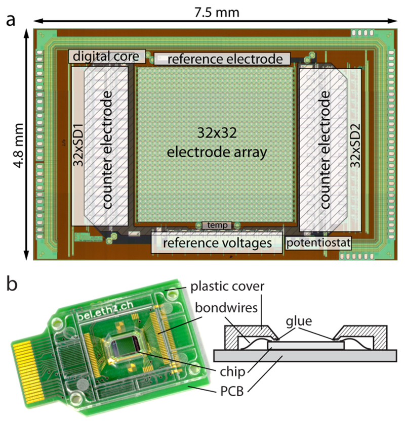
The system includes a custom-designed CMOS chip, a PCB hosting an FPGA, and a computer running a custom-made software suite (for a picture of the complete system, refer to Supporting Information SI-1). The major blocks of the CMOS chip architecture are shown in Figure 1a and include the sensor array, the master potentiostat, current ADCs (SD1 and SD2), and DACs. As all sensor signals and reference signals are digitized and generated on chip, the communication between chip and PCB is purely digital. The specifications of the system components are summarized in Table 1.
Figure 1.
(a) Micrograph of the CMOS chip with the main circuit blocks indicated. The platinum is patterned on top of the CMOS circuits; the SDCs thus are below the counter electrodes. (b) Picture and schematic cross-section of the packaged CMOS chip. Only the electrode array and counter and reference electrodes are exposed. The electric contacts and wire bonds are protected by an injection molded polycarbonate cover glued on the chip and PCB.
Table 1. Device Specifications.
| (A) Array of Electrodes | ||
| number of working electrodes | 1024 | 1024 |
| arrangement | 32 × 32 | 32 × 32 |
| pitch | 100 μm | 100 μm |
| Electrode Design | ||
| working electrodes | ø 25 μm | ø 5–50 μm |
| reference electrode | 594 900 μm2 | 594 900 μm2 |
| counter electrode | 7 489 300 μm2 | 7 489 300 μm2 |
| material | Pt | Pt |
| (B) Potentiostat | ||
| maximum potential range (CE-WE) | 0–3.3 V | |
| resolution | 2.8 mV | |
| RE voltage range | 0–2.8 V | |
| (C) Current ADC | ||
| 1st order SDCs | 32 | |
| full scale range | 1 nA to 10 μA | |
| bandwidth | 500 Hz | |
| 2nd order SDCs | 32 | |
| full scale range | 100 pA to 2 μA | |
| bandwidth | 1 kHz | |
Sensing Array
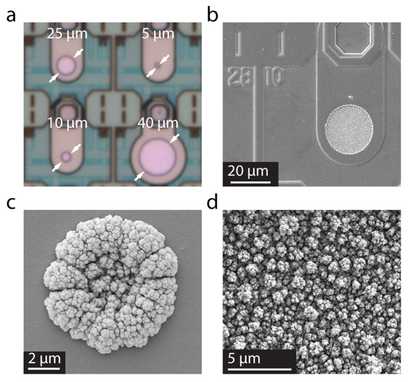
The array of working electrodes has been designed in two different layout versions. Both designs include an array of 32 by 32 electrodes. One design has equal-size electrodes of 25 μm diameter, to provide a large array of identical sensors. The other design includes electrodes with different diameters ranging from 5 to 50 μm in blocks of 4 × 8 electrodes (Figure 2 a), to explore applications, where the optimum electrode size is not a priori known. The electrodes have a center-to-center distance of 100 μm. A pseudoreference and a large counter electrode are located besides the array. Alternatively, a standard reference electrode and an external counter electrode can be used and connected to the CMOS chip via contact pads.
Figure 2.
(a) Microscopic picture of the platinum electrodes with different diameters. The white arrows denote the active area of the working electrodes. (b, c) Scanning electron micrographs of a 25 μm-diameter electrode (b) and 5 μm-diameter electrode (c) modified by Pt black. (d) Magnified cauliflower-like structure of the Pt black surface. (b, c, d) Picture: D. Mathys, Centre of Microscopy (ZMB), University of Basel Klingelbergstrasse 50/70, CH-4056 Basel.
Working electrodes in both designs are connected directly to an underlying 32-by-32 switch matrix. The electrodes can be accessed in two different modes; in the row-mode, arbitrary selected electrodes in each row of the array can be connected to one readout channel; in the block-mode, each electrode of an arbitrary chosen 4 × 8 subarray is connected to an individual readout channel allowing for continuous monitoring in a highdensity patch (see Supporting Information SI-3 for details). To acquire the current of all on-chip electrodes, the switch-matrix is operated in a multiplexing sequence (see below).
Multichannel Bipotentiostat
The core element, needed for electrochemical measurements, is the multichannel potentiostat. The potentiostat supports a three-electrode setup and includes a control loop that regulates the potential in the electrolyte and 64 current ADCs, which themselves independently control the potential of the working electrodes and are used to measure the current. The bipotentiostat is realized by the possibility to set the working electrodes to four different potentials. Thus, four different electrochemical regimes can be established at the same time.
The control loop to fix the potential in the electrolyte is realized by a two-stage amplifier with rail-to-rail input and output. The impedance of the working electrodes mainly determines the load, which the potentiostatic loop has to drive. Platinum electrodes in phosphate-buffered saline (PBS) have a characteristic capacitance of 20−50 μF/cm2, which sums up to 100−250 nF for 1024 disk electrodes of 25 μm diameter.37,38 The experimental conditions and the number of working electrodes that are used in an experiment may change considerably. In order to drive a wide range of loads at high stability, the amplifier is compensated with a large pole-splitting capacitor. Switches connect the amplifier to internal or external counter and reference electrodes.
Current Measurement
There are two different types of current ADCs implemented on the chip to set the potential of the working electrodes and to measure and digitize the current flowing through the electrodes (circuit diagram in Supporting Information SI-4).
One implementation is based on a first-order sigma-delta converter, which uses the double layer capacitance of the electrode in the electrolyte to integrate the charge.31 The converter consists only of a comparator, a flip-flop, and a switched-capacitor DAC to realize the sigma-delta loop. This loop keeps the voltage of the working electrode near the trigger voltage of the comparator by adding charge to or subtracting charge from the double layer capacitance. Operated at high frequencies (≫1 kHz), the average voltage at the input tracks the working electrode voltage (VWE).
The other current-readout implementation is a second-order sigma-delta converter that comprises two switched-capacitor integrators. In contrast to the first order SDC implementation, the amplifier of the first integrator here keeps the voltage of the working electrode fixed to VWE. In order to obtain a large voltage range, the amplifier has a rail-to-rail input stage.
A pair of switched capacitors is used to implement the 1-bit DAC of both sigma-delta converters. The current measured by the SDCs is defined by the DAC settings and can be determined by
for a sampling frequency of fs and with x denoting the averaged (decimated) bit stream value (−1 ≤ x ≤ 1). The reference voltage (Vref) and the value of the reference capacitor (Cref) define the charge that can be delivered by the capacitor per cycle and, thereby, the full scale range. The value of the measured current does not depend on the value of the double layer capacitance, which is an important prerequisite, since the double layer capacitance is unknown and depends on experimental conditions and operating region. The full-scale range is independent of the voltage at the charge delivery node (i.e., the working electrode), which allows for changing the voltage of the working electrode during the experiment, without altering the range.
With three different reference capacitor values (100 fF, 1 pF, and 10 pF) and the variable reference voltage and clock frequency, the first-order SDC can measure currents over a wide range (100 pA to 10 μA). The second-order SDC can be used to cover the full-scale range from 100 pA to about 2 μA (Cref = 200 fF or 2 pF, 0 < Vref < 2.8 V, 10 kHz < fs < 1.4 MHz), to detect currents down to 1 pA and to rapidly read out the currents of the whole array.
Taking “electrochemical images” by reading out the whole array is a central feature of the system. It is realized by using the second order sigma-delta converters in an incremental mode; i.e., upon conversion of one value, the integrators are reset for the next conversion cycle. The array is read out column by column. Electrodes, which are not connected to the readout, can be left floating or can be kept at a different potential by connecting them to the first-order SDC.
The first-order sigma-delta converter, additionally, can be used for measuring extremely high currents. Current densities from faradaic processes span a large range of 1 μA/cm2 to 100 mA/cm2.37,39 For a disk electrode of 25 μm diameter, this results in a current of 5 pA to 500 nA. Both current readout implementations together cover a range of 7 orders of magnitude. They also can be used in parallel for example to keep multiple electrodes passive, by applying a potential where no oxidation or reduction occurs, while other electrodes are active in an electrochemical procedure or detection scenario (use of functionalized sensors).
Measurement Setup
The chip is controlled by an FPGA via a digital serial interface. The FPGA (Xilinx Spartan 6) performs filtering of the data, controlling of automated tasks, such as running cyclic voltammograms (CVs), and data framing to transmit measurement data in packets to the computer via USB. The FPGA also controls the fast acquisition of measurements from the whole electrode array: initialization of the ADCs to start the conversion, definition of the connections in the array, and filtering of the acquired data.
The experiments are controlled via a graphical user interface programmed in LabVIEW (National Instruments). The recorded data sets have been analyzed in MATLAB (Math-Works).
Fabrication
The chip has a size of 7.5 × 4.8 mm2 and has been fabricated in a 2-polysilicon-4-metal layer 0.35 μm standard CMOS process (X-FAB, Erfurt, Germany). The platinum microelectrodes have been patterned on the chips during a wafer-level postprocessing in house. First, a SiO2 passivation layer has been deposited over the whole wafer. Reactive ion etching has been used to reopen the connection pads. An adhesion layer of WTi (50 nm) and the platinum layer (270 nm) have been deposited and structured through ionbeam deposition and ion-beam etching processes. Finally, a thick (1.6 μm) passivation stack, consisting of SiO2 and Si3N4, has been deposited on top of the wafer and has been structured by reactive ion etching to open the active areas of the electrodes (Figure 2 a; circular electrodes marked with arrows).
The single dies were mounted on PCBs and connected with wirebonds. To protect those wire bonds, an injection-molded part, made from polycarbonate, was glued onto the assembly (see Figure 1b). An additional larger reservoir for liquid samples could be clamped on top. The whole assembly was then plugged into the measurement setup (see Supporting Information SI-1).
Electric Characterization
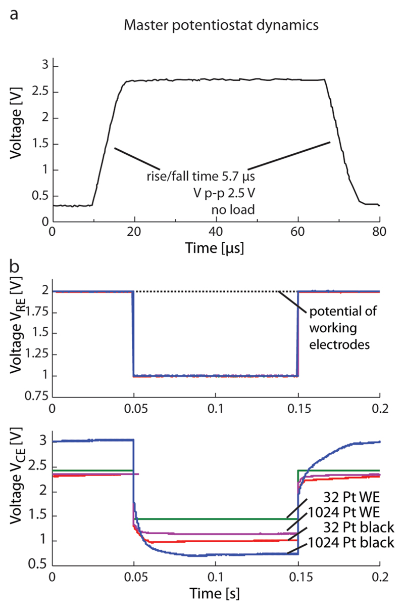
The dynamics of the master potentiostat were determined by applying a pulse of 2.5 V peak-to-peak under dry conditions through connecting the counter-electrode directly to the reference electrode. Functionality and stability were tested under dry conditions by connecting external capacitors (up to 100 μF) and in PBS with an external standard Ag/AgCl reference electrode and the on-chip platinum counter-electrode. In PBS, connecting different numbers of blank platinum working electrodes and Pt-blackcovered working electrodes provided the different load conditions. To test for stability, a square wave of 1 V vs Ag/AgCl was applied, and the voltages at the reference and counter electrodes were monitored.
To test the analog-to-digital converters, a sinusoidal current was generated by a voltage source (DS360 Stanford Research Systems, U.S.), connected in series to different resistors (1−100 MΩ), depending on the targeted range. To assess the performance of the first-order sigma-delta converters, PBS was used as an electrolyte to establish the double layer capacitance at the electrode, which is needed for the integration function. The electrodes were blank platinum electrodes; the voltage was set to 0 V vs Ag/AgCl. The electric characterization of the second order SDC was performed under dry conditions by using the same equipment as for the first order SDC. All tests were conducted without a Faraday cage to imitate real working conditions.
Functionalization Schemes
Prior to use, the chips were cleaned by recording multiple cyclic voltammograms in 1 M H2SO4 (−0.2 to 1.25 V vs Ag/AgCl, 50 mV/s, 10 cycles). To increase the effective surface area while maintaining a small geometric sensor area, a layer of amorphous platinum black was grown onto the bare platinum electrodes by applying a simple voltage-pulse-based deposition40 that relies on the use of on-chip circuitry and an external Ag/AgCl reference electrode (details in Supporting Information SI-9).
The protocol to functionalize the electrodes for detecting glucose41 involves electropolymerization of o-phenylenediamine together with glucose oxidase by cycling the applied voltage with the help of an external counter (Pt) and reference (Ag/AgCl) electrode (details in Supporting Information SI-9). The bipotentiostatic feature was used to keep the other electrodes at −0.1 V to reduce nonspecific adsorption. All experiments were done at room temperature.
Electrochemical Measurements
Cyclic voltammograms were recorded in 1 M H2SO4. The sweeps were performed from −0.2 to 1.25 V vs an external Ag/AgCl reference electrode at a sweep rate of 100 mV/s. The microscopic (true or active) electrode area was determined from the charge needed to remove an adsorbed monolayer of hydrogen atoms. It was determined by integrating the current in the corresponding region of the CV and by subtracting it from the current needed to charge the double layer capacitance. The true area is given by a characteristic charge of 208 μC/cm2.42
Electrochemical images have been acquired in PBS. An aliquot of H2O2 (1 μL of 30 mM into 3 mL of PBS) was injected with a microneedle into the liquid at the center of the array (~0.5 mm distance). Amperometric measurements to measure H2O2 concentration were done at 0.5 V vs an external Ag/AgCl reference electrode and by using the on-chip platinum counter electrode.
A calibration experiment to assess sensitivity was performed by using a simple fluidic PDMS chamber placed on the array. A syringe pump was used to pump different concentrations of H2O2 in PBS at a flow rate of 10 μL/s over the array. On-chip Pt counter and pseudoreference electrodes were used with the working electrodes being set to 700 mV.
For the glucose biosensor calibration, an external Pt counter and Ag/AgCl reference electrodes were used, and the working electrodes were set to 0.65 V vs Ag/AgCl for amperometric detection. Aliquots of glucose were added to PBS solution to provide different concentrations.
Results and Discussion
In the following section, the features and characteristics of the system will be demonstrated. First, the system and electronic characterizations will be presented. Then, electrochemical experiments will be shown and, finally, the array functions will be demonstrated for an exemplary use as glucose biosensor.
Sensing Array
The postprocessing concept enables a high flexibility in the layout of the electrodes that are located on top of the switch matrix (Figures 1 and 2). The possibility to vary the electrode sizes and layout renders the device suitable for a multitude of applications and enables one to study how the specific electrode area determines the recorded signals. Uniform electrodes of 25 μm diameter have been arranged to yield a large array of so-called ultramicroelectrodes.43
Multichannel Bipotentiostat
The master potentiostat was tested for speed and stability (Figure 3). The slew rate was determined to be 350 kV/s (Figure 3a) with the counter-electrode output and the reference-electrode input shorted. Having a high slew rate is a prerequisite for being able to provide steep square wave pulses as used in deposition protocols. For a pulse of 1 V amplitude, the slew rate of the amplifier adds a negligible 2.9 μs rise time.
Figure 3.
(a) Step response of the potentiostat without external load showing a slew rate of 350 kV/s. (b top) Voltage at the Ag/AgCl reference electrode for a step of 1 V under different load conditions (solid lines are on top of each other). Dashed line denotes the potential of the working electrodes. (b bottom) Corresponding voltage at the on-chip counter electrode controlled by the potentiostat for a load of 32 blank Pt (green curve), 1024 blank Pt (magenta curve), 32 Pt black (red curve), and 1024 Pt black (blue curve) working electrodes.
A mandatory system requirement is the control loop stability. An external capacitor of 1 μF entailed the smallest phase margin, which was 66°. The upper plot in Figure 3b shows the voltage of the Ag/AgCl reference electrode. When applying a square wave to the input, the response of the amplifier showed high stability and no ringing for very small loads, 32, 25 μm-diameter bright Pt electrodes and, for large loads, 1024 electrodes modified with Pt black.
The lower plot in Figure 3b shows the corresponding voltage at the counter electrode. The voltages at the counter electrode are usually not considered, because they are forced to a certain value by the potentiostatic loop in order to provide the preset potential at the reference electrode. However, one can see the effect of the different loading conditions on this voltage and the resulting requirements for the circuitry. When only 32 bright-platinum electrodes are connected, the current through the counter electrode is small and does not alter the interface, and as a result, the voltage at the electrode just reproduces the voltage at the reference electrode with some offset. When 1024 electrodes, modified with Pt black, are connected, the perturbation of the electrode interface of the counter electrode due to flowing currents is much larger, the peak-to-peak voltages are higher, and the voltage curve is not a simple reproduction of that at the reference electrode anymore. In a simplistic view, the counter electrode and the working electrodes form a capacitive divider. The large area, chosen for the counter electrode, lowers its impedance, thereby reducing the voltage overhead needed to provide a certain potential in the electrolyte. Nevertheless, the capability of the potentiostat to use the whole range of the 3.3 V power supply provides enough margin to work under higher load conditions, for example, during the deposition of Pt black.
Current Measurements
The performance of the two different SDC current-readout schemes is summarized in Table 2 for different range settings (details in Supporting Information SI-5).
Table 2. Electrical Characteristics of the Main Circuit Blocks.
| 1st Order Sigma-Delta Converter | ||||
| range | 1 μA | 100 nA | 10 nA | |
| bandwidth | 230 Hz | 230 Hz | 340 Hz | |
| ENOB | 11.9 bit | 10.1 bit | 6.8 bit | |
| 2nd Order Sigma-Delta Converter | ||||
| range | 1 μA | 100 nA | 10 nA | 1 nA |
| BW | 1 kHz | 1 kHz | 1 kHz | 130 Hz |
| int. RMS noise | 250 pA | 16.8 pA | 3.2 pA | 540 fA |
| ENOB | 13.3 bit | 11.6 bit | 10 bit | 7.9 bit |
| Potentiostat | ||||
| slew rate | 350 kV/s | |||
| sweep rate | 0–300 V/s | |||
The best signal-to-noise-and-dynamic-range ratio (SNDR) of the first-order sigma-delta (73.6 dB or 11.9 effective number of bits (ENOB)) is achieved for a range of ±1 μA (230 Hz BW).
The second-order SDC achieves an ENOB of up to 13.3 bits for a 1 kHz bandwidth and a range of ±1 μA full scale. The integrated noise for the lowest range (±100 pA) is 220 fA within a bandwidth of 100 Hz (21.5 fA/√Hz). The second-order sigma-delta converter has a much higher resolution and bandwidth, compared to the first-order SDC, owing to the better noise shaping and the active integrator structure. High resolution is required to reveal small signals embedded in a large background current.
Cyclic Voltammetry
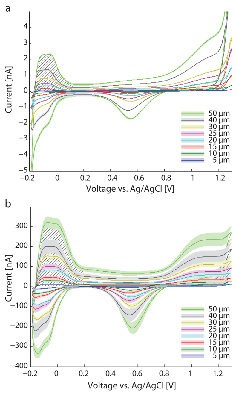
Figure 4 shows cyclic voltammograms in 1 M H2SO4 for bare platinum electrodes of different electrode diameters (Figure 4a) and for electrodes modified with Pt black (Figure 4b). The CVs show the characteristic features of a polycrystalline platinum electrode in H2SO4 and the buildup of adsorption layers of oxygen and hydrogen as well as their removal and bulk solution electrolysis. The CVs do not show any indication of contamination resulting from metals (Al, Cu) of the CMOS layers.
Figure 4.
Cyclic voltammograms in 1 M H2SO4 at 100 mV/s sweep rate. (a) Blank platinum electrodes, (b) after deposition of Pt black. Hatched areas show the areas used to calculate the microscopic surface area.
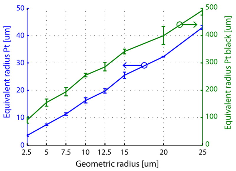
The hatched area in Figure 4 marks the region, from which the microscopic electrode area was determined. An equivalent radius was calculated from the microscopic area, which would be the radius of an equivalent electrode with a perfectly smooth surface. It is plotted in Figure 5 for blank platinum electrodes (left ordinate) and Pt black electrodes (right ordinate) for comparison. The roughness factor is determined by the ratio of the microscopic area to geometric area. For blank platinum electrodes, the mean roughness factor is 1.97 ± 0.29 (n = 32, ± standard deviation). The uniformity of the blank platinum electrodes, evidenced by the roughness factors, shows the precision of the microtechnological processing steps and allows for performing reproducible measurements. Electrodeposition of Pt black, on the other hand, increases the active area by a factor of >100 for the large, 50 μm diameter electrodes, and a factor of >400 for the small, 5 μm diameter electrodes. The mean roughness factor, where Pt black was deposited, is 540, however, with a standard deviation of ±267 (n = 32). In Figure 2, SEM images are shown from a 25 μm (b, d) and 5 μm (c) electrode after deposition of Pt black. The increase in roughness factor is not uniform, when differently sized electrodes are functionalized with the same protocol, which has to be taken into account by making calibration measurements.
Figure 5.
Geometric vs equivalent radius of the electrode, calculated from the microscopic area as determined in Figure 4. The equivalent radii of blank Pt electrodes relate to the ordinate at the left; those of electrodes with Pt black to that at the right.
Electrochemical Images
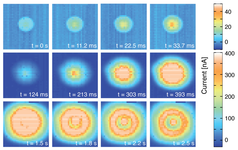
An amperometric electrochemical image sequence from all 1024, 25 μm-diameter electrodes of the array has been acquired (Figure 6 and video in Supporting Information SI-6). The image sequence shows the injection of an aliquot of H2O2 (1 μL, 30 mM) via a syringe into PBS (3 mL) atop the electrode array and subsequent liquid-phase transport of the H2O2 molecules across the array area. The first row in Figure 6 contains images from consecutive frames of the video showing the beginning of the injection of peroxide. The pictures in the following rows are extracted from the video at different points later in time. The wave of the H2O2 molecules, traveling at a speed of 2.2 mm/s to the corners of the array, can be clearly resolved. The images were taken at 89 frames per second (fps), which means that more than 91 000 sensor current values have been read out per second from an area of 3.2 by 3.2 mm2. Compared to image sequences acquired by electrochemical CMOS microarrays shown in previous publications, this is more than double the frame rate for 10 times more electrodes (10 × 10 electrodes at 40 fps28) and more than double the number of electrodes for more than 15 times the frame rate (20 × 20 electrodes at 5 fps20,29). The high temporal and spatial resolution allows for tracking liquid-phase diffusion and convection processes.
Figure 6.
Image sequence of amperometric measurement at 0.5 V vs an external Ag/AgCl reference electrode showing the distribution of an aliquot of H2O2 injected in the center of the liquid phase over the array, taken at a frame rate of 89 fps. Electrodes were modified by depositing Pt black. The image size corresponds to an area of 3.2 by 3.2 mm2.
Sensitivity and Limit of Detection
The mean sensor sensitivity to H2O2 is 4.5 nA/μM, with a theoretical limit of detection of 13 nM (calculated by using 3 times the background noise). A raw trace can be seen in the Supporting Information (SI-7).
Parallel Biosensing of Glucose
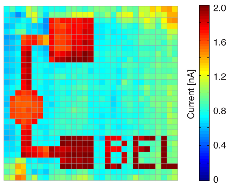
As an exemplary biosensor application, an array with 1024, 25 μm electrodes was modified to monitor glucose. The electrochemistry-based deposition method allowed one to functionalize only selected electrodes, so as to display the logo of our lab. The possibility of spatial controlled electrode modification or functionalization is an important issue for large arrays, especially when several electrodes have to be modified differently. Figure 7 shows the amperometric current increases only at the specifically functionalized electrodes upon addition of 1 mM glucose in the solution on top of the array. The sensitivity is 1.87 ± 0.18 nA/mM (mean ± std, n = 217; see also Supporting Information SI-8). The nonoptimized deposition protocol also leads to some nonspecific adsorption of the enzyme at nonfunctionalized electrodes, which, however, produce significantly lower signals. The glucose sensors could be used for up to a week on average by storing them in PBS at room temperature.
Figure 7.
Addition of 1 mM of glucose to an array, on which only a defined number of electrodes were functionalized with glucose oxidase to form the logo of our lab.
Conclusion
We have reported on a versatile CMOS-based electrode array system, which can be used to perform voltammetry and amperometry on up to 1024 electrodes in parallel. The system takes maximal advantage of the use of CMOS technology. First, the generation and digitization of all analogue signals on the chip improves signal quality, as no weak analogue signals have to be transmitted off chip, and helps to overcome the routing problem through digital multiplexing. This allowed us to increase the frame rate up to 90 fps for 1024 electrodes and enables the acquisition of electrochemical measurements at subsecond resolution so that, e.g., diffusion processes in liquid phase can be precisely tracked. Owing to the integrated high-resolution ADCs (>13 bit), small signals in a large background current can be resolved, and electrochemical images from a large number of electrodes can be taken. Second, the system circuits have been designed to effectively address the problem of limited currents in electrochemical setups with microelectrode arrays. A large current range of 10 μA down to 100 pA is available that not only can be used for electrodeposition and functionalization of the electrodes but also enables one to detect low analyte concentrations. The integrated noise of 220 fA in a bandwidth of 100 Hz allows for detection of pA currents. Further, the circuitry allows for one to handle large and varying double layer capacitances, of electrodes immersed in an electrolyte so that the full spectrum of electrochemical detection and deposition protocols can be used with the chip. The microtechnological fabrication of the array of platinum yields very uniform electrode characteristics. The chip package reliably protects the circuitry against the liquid phase and provides containment for sample and liquid handling. The system setup and user interface allow one to perform and control automated experiments and perform data analysis. Future applications will be targeted at biological systems, such as the detection of neurotransmitters in brain slice preparations, metabolic activity in cell cultures, or secretion of marker molecules of single cells at high temporal and spatial resolution.
Supplementary Material
This material is available free of charge via the Internet at http://pubs.acs.org.
Acknowledgments
This work has been financially supported by the European Community through the ERC Advanced Grant 267351 “NeuroCMOS”. We acknowledge the ZMB (Zentrum für Mikroskopie) of the University of Basel, Switzerland, for taking the SEM pictures (Figure 2) and Rajtarun Madangopal, Purdue University, for help with optimizing the Pt black deposition protocol.
Footnotes
Notes
The authors declare no competing financial interest.
References
- (1).Bakker E. Anal Chem. 2004;76:3285–3298. doi: 10.1021/ac049580z. [DOI] [PubMed] [Google Scholar]
- (2).Wang J. Biosens Bioelectron. 2006;21:1887–1892. doi: 10.1016/j.bios.2005.10.027. [DOI] [PubMed] [Google Scholar]
- (3).Ronkainen NJ, Halsall HB, Heineman WR. Chem Soc Rev. 2010;39:1747–1763. doi: 10.1039/b714449k. [DOI] [PubMed] [Google Scholar]
- (4).Robinson DL, Hermans A, Seipel AT, Wightman RM. Chem Rev. 2008;108:2554–2584. doi: 10.1021/cr068081q. [DOI] [PMC free article] [PubMed] [Google Scholar]
- (5).Heien MLAV, Johnson MA, Wightman RM. Anal Chem. 2004;76:5697–5704. doi: 10.1021/ac0491509. [DOI] [PubMed] [Google Scholar]
- (6).Hochstetler SE, Puopolo M, Gustincich S, Raviola E, Wightman RM. Anal Chem. 2000;72:489–496. doi: 10.1021/ac991119x. [DOI] [PubMed] [Google Scholar]
- (7).Wightman RM. Science. 2006;311:1570–1574. doi: 10.1126/science.1120027. [DOI] [PubMed] [Google Scholar]
- (8).Ino K, Kanno Y, Nishijo T, Komaki H, Yamada Y, Yoshida S, Takahashi Y, Shiku H, Matsue T. Anal Chem. 2014;86:4016–4023. doi: 10.1021/ac500435d. [DOI] [PubMed] [Google Scholar]
- (9).Amatore C, Arbault S, Guille M, Lemaître F. Chem Rev. 2008;108:2585–2621. doi: 10.1021/cr068062g. [DOI] [PubMed] [Google Scholar]
- (10).Liu X, Barizuddin S, Shin W, Mathai CJ, Gangopadhyay S, Gillis KD. Anal Chem. 2011;83:2445–2451. doi: 10.1021/ac1033616. [DOI] [PMC free article] [PubMed] [Google Scholar]
- (11).Zhang B, Adams KL, Luber SJ, Eves DJ, Heien ML, Ewing AG. Anal Chem. 2008;80:1394–1400. doi: 10.1021/ac702409s. [DOI] [PMC free article] [PubMed] [Google Scholar]
- (12).Picollo F, Gosso S, Vittone E, Pasquarelli A, Carbone E, Olivero P, Carabelli V. Adv Mater. 2013;25:4696–4700. doi: 10.1002/adma.201300710. [DOI] [PubMed] [Google Scholar]
- (13).Kisler K, Kim BN, Liu X, Berberian K, Fang Q, Mathai CJ, Gangopadhyay S, Gillis KD, Lindau M. J Biomater Nanobiotechnol. 2012;3:243–253. doi: 10.4236/jbnb.2012.322030. [DOI] [PMC free article] [PubMed] [Google Scholar]
- (14).Drummond TG, Hill MG, Barton JK. Nat Biotechnol. 2003;21:1192–1199. doi: 10.1038/nbt873. [DOI] [PubMed] [Google Scholar]
- (15).Wang J. Anal Chim Acta. 2002;469:63–71. [Google Scholar]
- (16).Kalantari R, Cantor R, Chen H, Yu G, Janata J, Josowicz M. Anal Chem. 2010;82:9028–9033. doi: 10.1021/ac102002k. [DOI] [PubMed] [Google Scholar]
- (17).Levine PM, Gong P, Levicky R, Shepard KL. IEEE J Solid-State Circuits. 2008;43:1859–1871. [Google Scholar]
- (18).Kruppa P, Frey A, Kuehne I, Schienle M, Persike N, Kratzmueller T, Hartwich G, Schmitt-Landsiedel D. Biosens Bioelectron. 2010;26:1414–1419. doi: 10.1016/j.bios.2010.07.070. [DOI] [PubMed] [Google Scholar]
- (19).Augustyniak M, Paulus C, Brederlow R, Persike N, Hartwich G, Schmitt-Landsiedel D, Thewes R. 2006 IEEE International Conference Digest of Technical Papers Solid-State Circuits; New York: IEEE; 2006. pp. 59–68. [Google Scholar]
- (20).Inoue KY, Matsudaira M, Kubo R, Nakano M, Yoshida S, Matsuzaki S, Suda A, Kunikata R, Kimura T, Tsurumi R, Shioya T, et al. Lab Chip. 2012;12:3481–3490. doi: 10.1039/c2lc40323d. [DOI] [PubMed] [Google Scholar]
- (21).Mason A, Huang Y, Yang C, Zhang J. 2007 IEEE International Symposium on Circuits and Systems; New York: IEEE; 2007. pp. 3562–3565. [Google Scholar]
- (22).Manickam A, Singh R, Wood N, Li B, Ellington A, Hassibi A. 2012 Symposium on VLSI Circuits (VLSIC); New York: IEEE; 2012. pp. 126–127. [Google Scholar]
- (23).Hwang S, LaFratta CN, Agarwal V, Yu X, Walt DR, Sonkusale S. IEEE Sens J. 2009;9:609–615. [Google Scholar]
- (24).Martin SM, Gebara FH, Larivee BJ, Brown RB. IEEE J Solid-State Circuits. 2005;40:2777–2786. [Google Scholar]
- (25).Bellin DL, Sakhtah H, Rosenstein JK, Levine PM, Thimot J, Emmett K, Dietrich LEP, Shepard KL. Nat Commun. 2014;5:3256. doi: 10.1038/ncomms4256. [DOI] [PMC free article] [PubMed] [Google Scholar]
- (26).Schienle M, Paulus C, Frey A, Hofmann F, Holzapfl B, Schindler-Bauer P, Thewes R. IEEE J Solid-State Circuits. 2004;39:2438–2445. [Google Scholar]
- (27).Nazari MH, Mazhab-Jafari H, Leng L, Guenther A, Genov R. IEEE Trans Biomed Circuits Syst. 2013;7:338–348. doi: 10.1109/TBCAS.2012.2203597. [DOI] [PubMed] [Google Scholar]
- (28).Kim BN, Herbst AD, Kim SJ, Minch BA, Lindau M. Biosens Bioelectron. 2013;41:736–744. doi: 10.1016/j.bios.2012.09.058. [DOI] [PMC free article] [PubMed] [Google Scholar]
- (29).Sen M, Ino K, Inoue KY, Arai T, Nishijo T, Suda A, Kunikata R, Shiku H, Matsue T. Biosens Bioelectron. 2013;48:12–18. doi: 10.1016/j.bios.2013.03.069. [DOI] [PubMed] [Google Scholar]
- (30).Mazhab-Jafari H, Soleymani L, Genov R. IEEE Trans Biomed Circuits Syst. 2012;6:468–478. doi: 10.1109/TBCAS.2012.2226334. [DOI] [PubMed] [Google Scholar]
- (31).Heer F, Keller M, Yu G, Janata J, Josowicz M, Hierlemann A. 2008 IEEE International Solid-State Circuits Conference - Digest of Technical Papers; New York: IEEE; 2008. pp. 168–604. [Google Scholar]
- (32).Rothe J, Lewandowska MK, Heer F, Frey O, Hierlemann A. J Micromech Microeng. 2011;21:054010. [Google Scholar]
- (33).Stanacevic M, Murari K, Rege A, Cauwenberghs G, Thakor NV. IEEE Trans Biomed Circuits Syst. 2007;1:63–72. doi: 10.1109/TBCAS.2007.893176. [DOI] [PubMed] [Google Scholar]
- (34).Roham M, Daberkow DP, Ramsson ES, Covey DP, Pakdeeronachit S, Garris PA, Mohseni P. IEEE Trans Biomed Circuits Syst. 2008;2:3–9. doi: 10.1109/TBCAS.2008.918282. [DOI] [PubMed] [Google Scholar]
- (35).Mollazadeh M, Murari K, Cauwenberghs G, Thakor NV. IEEE Trans Biomed Circuits Syst. 2009;3:388–397. doi: 10.1109/TBCAS.2009.2031877. [DOI] [PubMed] [Google Scholar]
- (36).Rothe J, Frey O, Stettler A, Chen Y, Hierlemann A. 2012 IEEE Sensors. IEEE; New York: 2012. pp. 1–4. [Google Scholar]
- (37).Bockris JO, Reddy AKN, Gamboa-Aldeco ME. Modern Electrochemistry 2A Fundamentals of Electrodics. 2nd ed. Springer; Berlin Heidelberg: 2000. p. 763. [Google Scholar]
- (38).Franks W, Schenker I, Schmutz P, Hierlemann A. IEEE Trans Biomed Eng. 2005;52:1295–1302. doi: 10.1109/TBME.2005.847523. [DOI] [PubMed] [Google Scholar]
- (39).Hamann CH, Hamnett A, Vielstich W. Electrochemistry. 2nd ed. Wiley-VCH Verlag GmbH & Co. KGaA; Hoboken, NJ: 2007. p. 550. [Google Scholar]
- (40).Feltham AM, Spiro M. Chem Rev. 1971;71:177–193. [Google Scholar]
- (41).Lowry JP, McAteer K, El Atrash SS, Duff A, O’Neill RD. Anal Chem. 1994;66:1754–1761. [Google Scholar]
- (42).Doña Rodríguez JM, Herrera Melián JA, Perez Peña J. J Chem Educ. 2000;77:1195. [Google Scholar]
- (43).Bard AJ, Faulkner LR. Electrochemical methods: Fundamentals and applications. 2nd ed. Wiley; New York: 2001. p. 833. [Google Scholar]
Associated Data
This section collects any data citations, data availability statements, or supplementary materials included in this article.


