Abstract
The C 1s signal from ubiquitous carbon contamination on samples forming during air exposure, so called adventitious carbon (AdC) layers, is the most common binding energy (BE) reference in X‐ray photoelectron spectroscopy studies. We demonstrate here, by using a series of transition‐metal nitride films with different AdC coverage, that the BE of the C 1s peak varies by as much as 1.44 eV. This is a factor of 10 more than the typical resolvable difference between two chemical states of the same element, which makes BE referencing against the C 1s peak highly unreliable. Surprisingly, we find that C 1s shifts correlate to changes in sample work function , such that the sum is constant at 289.50±0.15 eV, irrespective of materials system and air exposure time, indicating vacuum level alignment. This discovery allows for significantly better accuracy of chemical state determination than offered by the conventional methods. Our findings are not specific to nitrides and likely apply to all systems in which charge transfer at the AdC/substrate interface is negligible.
Keywords: analytical methods, binding energy, surface analysis, surface chemistry, X-ray photoelectron spectroscopy
X‐ray photoelectron spectroscopy (XPS) is an essential analytical tool in surface science and materials research, providing information about surface chemistry and composition. The first observation of chemical shifts between Cu atoms in metallic and oxidized state,1 followed by a report on a S 1s peak split in the photoelectron spectrum of sulfur atoms in thiosulfate,2 shortly after, carbon atoms in 1,2,4,5‐benzenetetracarboxylic acid,3 and the whole range of N‐containing organic molecules,4 laid grounds for chemical analysis by electron spectroscopy (ESCA).5, 6 The unambiguous bonding assignment relies, however, on the correct measurement of binding energy (BE) values. This is often a nontrivial task because of the lack of an internal BE reference.7 During the XPS experiments the negative charge continuously removed from the surface region as a result of a photoelectric effect has to be replenished with a sufficiently high rate to preserve charge neutrality. If this condition is not fulfilled, the surface acquires positive potential, which decreases the kinetic energy of escaping photoelectrons, and in consequence leads to the apparent shift of all core level peaks towards higher BE; the phenomenon commonly referred to as charging. Since the specimen's charging state is not known a priori, the problem with correct BE referencing arises for the vast majority of samples. The natural zero of the BE scale exists only for specimens, in which the density of states (DOS) exhibits a well‐defined cut‐off at the Fermi energy E F, the so‐called Fermi edge, as is the case for metals in which high conductivity ensures Fermi level alignment between the sample and the spectrometer. All other samples that lack an internal BE reference present a serious challenge, which is reflected by a large spread of reported BE values for the same chemical state.8 Some examples include TiO2 with the reported Ti 2p3/2 and O 1s peak positions varying from 458.0 to 459.6 eV, and from 529.4 to 531.2 eV, respectively. In a similar way, for Si3N4, Si 2p and N 1s peaks have been reported at BE varying from 100.6 to 102.1 eV, and 397.4 to 398.6 eV, respectively.8 It is highly disturbing that after more than 50 years of development, the BE of constituting elements in many technologically relevant materials is accessed with an accuracy that is not better than the magnitude of typical large chemical shifts of the order of 1 eV, much larger than the instrument resolution at 0.1 eV (or less), which makes the bonding assignment ambiguous, often leading to an arbitrary spectra interpretation and contradicting results.
The situation is worsened by the fact that the use of a natural BE reference such as the Fermi edge in the case of conducting samples, is not at all common. This is again reflected by the spread of reported BE values, not as large as for insulators, yet significant enough to often prevent correct bonding assignment. For example, in the case of transition‐metal (TM) nitrides, which exhibit pronounced DOS at the Fermi level and, hence, metallic‐like conductivity, reported BE values for core level signals often differ by more than 1 eV; the Ti 2p3/2 core level of TiN varies from 454.77 to 455.8 eV, whereas the position of the N 1s peak changes by 0.9 eV for TiN, and 1.2 eV for ZrN, MoN, and NbN.
It has become a common procedure to use the C 1s signal from the adventitious carbon (AdC) layer present on the vast majority of surfaces following air exposure, as a BE reference. To calibrate the BE scale the C−C/C−H peak of AdC is deliberately set at 284.0–285.2 eV and all core‐level spectra are aligned accordingly.9 The method was first proposed by Siegbahn et al.6 in the early days of XPS applications and was originally based on the observation that the AdC layer is present on all air‐exposed surfaces with the C 1s line as it appeared constant at 285.0 eV, which made it an ideal candidate for BE referencing.10 Soon after, however, the claim was dropped, as it became clear that the C 1s BE in practice varies with the thickness of the hydrocarbon layer by as much as 0.6 eV for Pd and Au substrates.11, 12 In the review of existing literature published in 1982, Swift concluded that “although the use of C 1s electrons from adventitious carbon layers is often a convenient method of energy referencing, interpretation of binding energy data obtained should be treated with caution”.9 In the following years, problems with using the C 1s peak for BE referencing accumulated. For example, Werrett et al. reported inconsistent results when referencing to C 1s of AdC during studies of oxidized Al‐Si alloys, which was due to the oxidation of AdC,13 whereas Gross et al. showed that the Au 4f signal from gold particles deliberately deposited on amorphous SiO2 provides more reliable BE reference than C 1s.14 More recent examples indicate that the issue of correct referencing of XPS spectra remains unresolved,15, 16 which contrasts with the fact that the method based on adventitious carbon is widely adopted.
Our literature review shows that in 58 of the first 100 top‐cited papers dealing with XPS studies of magnetron sputtered films published between 2010 and 2016 in peer‐reviewed journals, C 1s of AdC was used as a BE reference,17 whereas, alarmingly, the remaining papers lack information about any referencing method used. Within the first group, the C 1s peak was set quite arbitrary at the BE, varying from 284.0 to 285.2 eV (here we disregard two extreme cases of 283.0 and 298.8 eV). This serious inconsistency easily accounts for the large spread of reported BE values for the same chemical species (see examples above), and contradicts the notion of the BE reference, which per definition should be associated with one single energy value (as was originally intended in ref. 6).
Here, we examine the reliability of using AdC for XPS BE referencing by measuring the position of the C 1s peak for a series of TM nitride thin‐film layers that exhibit a well‐defined Fermi edge cut‐off serving as an internal BE reference. Measurements are performed as a function of the AdC layer thickness, which scales with the air exposure time. We show that the BE of the C 1s peak of AdC measured with respect to the Fermi edge varies by as much as 1.44 eV, from 284.08 eV in the case of MoN to 285.52 eV for a HfN sample. This is a factor of 10 more than the typical resolvable difference between two chemical states of the same element, which makes the energy referencing against the C 1s peak of AdC highly unreliable. Moreover, we demonstrate that the position of the C 1s peak of AdC closely follows changes in sample work function , assessed here by ultraviolet photoelectron spectroscopy (UPS), in such a way that the sum is essentially constant at 289.50±0.15 eV, which corresponds well to the gas‐phase BE value of longer alkanes lowered by the intermolecular relaxation energy. This indicates that C 1s aligns to the vacuum level , and implies that its BE is steered by the sample work function. Clearly, the C 1s of AdC cannot be used for reliable BE referencing of XPS spectra in a conventional way, unless a complementary measurement of is performed and C 1s is set at 289.50− . We show that this approach results in a considerably better accuracy of chemical state determination as compared with the status quo.
The ubiquitous nature of AdC has been analyzed in detail by Barr et al.,18 who concluded that it predominantly consists of polymeric hydrocarbon species (C−C/C−H), together with a minor component (10–30 % of the total signal intensity) due to carbooxides containing C−O−C and O−C=O bonds. Indeed, a set of C 1s core level spectra acquired from (TM)N surfaces in the as‐received state (see Figure 1) reveals that carbon is present in several chemical states almost on every surface analyzed. In all cases, however, the spectra are dominated by the aliphatic carbon C−C/C−H peak, whereas C−O−C and O−C=O contributions present at higher BE appear in much lower concentrations. Clearly, there is a substantial change in the C 1s spectra appearance depending on the (TM)N studied. Not only do the number of component peaks change (e.g., no O−C=O peak is observed in the present case of WN and MoN), but, more importantly, the BE of the dominant C−C/C−H peak, measured with respect to the Fermi level of the spectrometer , exhibits large variation: from 284.08 eV in the case of MoN surface to 285.52 eV for HfN, as summarized in Table 1. The 1.44 eV change in the position of the C 1s peak is certainly disturbing, as one would clearly expect the BE of carbon species present in the same chemical state to be independent of the underlying substrate, especially if used for referencing XPS spectra.
Figure 1.
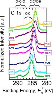
C 1s XPS spectra of adventitious carbon obtained from as‐received air‐exposed (ca. 10 min.) polycrystalline (TM)N thin films, where TM=Mo, V, W, Ti, Cr, Nb, Ta, Zr, and Hf, grown by magnetron sputtering on Si(001) substrates.
Table 1.
Binding energies relative to Fermi level for all component peaks in C 1s spectra together with work function values obtained from polycrystalline (TM)N thin films in the as‐received state, where TM=Mo, V, W, Ti, Cr, Nb, Ta, Zr, and Hf.
| (TM)N | C 1s BE relative to Fermi level, [eV] | ΔBE CC−O−CC−C | ΔBE CO−C=O−CC−C | Work function [eV] | ||
|---|---|---|---|---|---|---|
| C−C/C−H | C−O | O−C=O | ||||
| TiN | 284.52 | 286.24 | 289.06 | 1.72 | 4.54 | 4.90 |
| VN | 284.15 | 285.96 | 288.51 | 1.81 | 4.36 | 5.16 |
| CrN | 284.60 | 286.14 | 288.56 | 1.54 | 3.96 | 4.83 |
| ZrN | 285.49 | 287.21 | 289.54 | 1.72 | 4.05 | 4.09 |
| NbN | 284.76 | 286.52 | 289.18 | 1.76 | 4.42 | 4.65 |
| MoN | 284.08 | 285.76 | – | 1.68 | – | 5.35 |
| HfN | 285.52 | 287.17 | 289.75 | 1.65 | 4.23 | 4.00 |
| TaN | 285.08 | 286.75 | 289.39 | 1.67 | 4.31 | 4.41 |
| WN | 284.22 | 285.73 | – | 1.71 | – | 5.23 |
The C 1s contribution due to C−O also shifts from sample to sample, from 285.76 eV for as‐received MoN to 287.21 for ZrN (1.45 eV difference), essentially following the C−C/C−H peak, so that the relative BE difference Δ(CC−O−CC−C) is nearly constant at 1.70±0.13 eV (cf. Table 1). The BE of the O−C=O peak does not follow the shifts observed for all other C 1s contributions, which is best seen by comparing the C 1s spectra recorded from TiN and CrN surfaces, see Figure 1, and varies from 288.51 eV for VN to 289.75 eV for HfN (1.24 eV difference). Some C 1s spectra (TiN, ZrN) possess also an extra contribution at significantly lower BE (282.0–282.5 eV), which is assigned to carbide formation during film growth,19 and as such is of minor importance for this work.
The amount of AdC that accumulates on the surface of (TM)N films exhibits a steady increase with the air exposure time, as illustrated in Figure 2, in which surface C concentrations are plotted for all nitride samples in the time span from 10 minutes to 7 months. Even though the percentage amount of AdC varies somewhat between different samples, the accumulation rate is essentially the same and amounts to ca. 5 at % per decade. The corresponding evolution of of the dominant C−C/C−H C 1s peak of AdC with air exposure time is shown in Figure 3 (a). Interestingly, even though there is a certain variation in C 1s for each materials system (rather random and not exceeding 0.5 eV), a large spread in BE of the C 1s peak observed for samples in the as‐received state persists for layers that were sputter‐cleaned and subsequently exposed to ambient atmosphere for time periods varying from 10 minutes to 7 months. Thus, we can conclude that the template dependence of C 1s BE takes place irrespective of the amount of accumulated adventitious carbon. We note also that changes in the BE′s of the intrinsic core level signals (metal and nitrogen peaks) during prolonged air exposure are lower than 0.1 eV.
Figure 2.
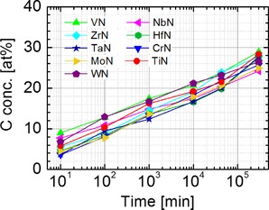
Surface carbon concentrations plotted as a function of air exposure time for polycrystalline (TM)N thin films, where TM=Mo, V, W, Ti, Cr, Nb, Ta, Zr, and Hf, grown by magnetron sputtering on Si(001) substrates.
Figure 3.
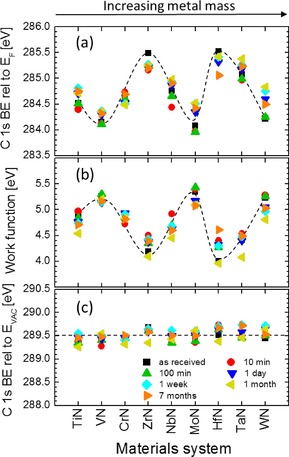
a) Binding energy of the C−C/C−H peak in the C 1s spectra of adventitious C referenced to Fermi level , b) work function obtained by UPS from the secondary electron cut‐off , and c) C 1s BE referenced to Vacuum level for a set of polycrystalline (TM)N thin films, where TM=Mo, V, W, Ti, Cr, Nb, Ta, Zr, and Hf, grown by magnetron sputtering on Si(001) substrates. The dashed curves in (a) and (b) are only for eye guiding to emphasize the symmetry between the plots.
To address the issue of C 1s shifts, we first obtain a reliable evaluation of the charging state of the actual (TM)N film. To do this, we record DOS in the vicinity of the Fermi edge (Fermi level cut‐off). Electrons close to E F possess the highest kinetic energy of all excited photoelectrons (essentially equal to ), which results in relatively long mean free path λ, from to 18 to 24 Å.20 In consequence, the XPS probing depth, given by 3×λ, well exceeds the thickness of the AdC layer, which is in the range 4.5–9 Å. This, together with the fact that adventitious carbon being a wide band gap material does not possess DOS near E F,18 implies that the spectral intensity in this region is solely determined by the TM(N). Figure 4 (a) shows the Fermi level cut‐off for all TM(N) samples in the as‐received state, as measured. In all cases, the rapid drop in DOS coincides with “0” of the BE scale, which is indicative of a Fermi level alignment between sample and the spectrometer. This proves that a good electrical contact is established to the instrument and excludes any possibility of charging in the (TM)N layer.
Figure 4.
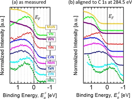
The portion of the valence band spectra in the close vicinity of the Fermi level EF indicating the Fermi level cut‐off for as‐received polycrystalline (TM)N thin films, where TM=Mo, V, W, Ti, Cr, Nb, Ta, Zr, and Hf, grown on Si(001) substrates: a) as measured (referencing to E F), and b) aligned by using the common procedure of referencing to C 1s peak of adventitious carbon set at 284.5 eV.
The fact that C 1s shifts (cf. Figure 1) while the Fermi edge from the underlying (TM)N film appears at “0” eV (Figure 4 (a)) clearly indicates decoupling of the measured energy levels of adventitious carbon from the Fermi level of the underlying substrate and, hence, spectrometer. The implications for BE referencing that employs the C 1s peak are severe. If, as commonly practiced, one would align all recorded spectra by setting the C−C/C−H peak of AdC at 284.5 eV, the highest portion of the valence band spectra recorded from (TM)N appears as shown in Figure 4 (b). Contrafactory, some specimens (TiN, VN) would exhibit no DOS at E F despite their metallic character, whereas for other films (HfN, ZrN, and TaN) such calibration of the BE scale results in a non‐zero DOS above the Fermi level. These examples demonstrate that the common procedure of referencing to the C 1s level set at the arbitrary chosen BE value within the range, 284.0–285.2 eV, is not justified because it leads to unphysical results. The latter is not realized if dealing with core level spectra, in which case shifts in peak positions by ±1 eV do not lead to such clear contradictions.
To gain more insight into the energy level alignment at the AdC/(TM)N interface, we perform measurements of sample work function in the same instrument; that is, without breaking the vacuum. As summarized in Figure 3 (b), in which sample work function is plotted for all TM(N) layers in the order of an increasing TM mass, and for various amounts of air exposure time, exhibits large apparent variations, that in the case of as‐received samples range from 4.00 eV for HfN to 5.35 eV for MoN. More importantly, a direct comparison to the values shown in Figure 3 (a) reveals that the trend in work function closely correlates to that observed for the C 1s peak of AdC, such that the sum remains constant for all samples, irrespective of air exposure time at 289.50±0.15 eV (see Figure 3 (c)). This implies that C 1s aligns to the vacuum level ,21, 22 rather than to the Fermi level, as is implicitly assumed when using this peak for BE referencing. Hence, the position of the C 1s peak measured with respect to E F is steered by the substrate work function, which disqualifies this signal as a reliable reference, unless a complementary measurement of is performed and spectra are aligned to C 1s set at 289.50− eV. The position of the C 1s C−C/C−H peak referenced to , 289.50 eV, corresponds very well with the gas‐phase value of 290.15 eV measured for longer alkanes by Pireaux et al.,23 compensated for the intermolecular relaxation energy due to electronic and atomic polarization of the neighboring molecules surrounding the core hole, which is typically of the order of 1–3 eV.24
The vacuum level alignment is characteristic of a weak interaction at the interface to the substrate and is regularly observed for organic films deposited on metals by using ex‐situ techniques (e.g. spin coating) in the absence of both charge transfer across the interface and interface dipole formation.25 Such contacts remain within the Schottky–Mott limit, in which the electronic levels of the adsorbate are determined by the work function of the substrate.26 As a matter of fact, the process of AdC adsorption is also classified as physical,18 because the principal species (hydrocarbons) are not chemically reactive and can be readily desorbed by a gentle anneal in vacuum.27 In the present case, the potential interaction between AdC species and (TM)N film is further suppressed by the presence of a native oxide layer.
Our findings are schematically summarized in Figure 5, in which the relevant energy levels and critical parameters are indicated for (a) a low work function sample, and (b) a high work function sample. Independent of we find that the Fermi level cut‐off of (TM)N aligns with that of the spectrometer (which is established during the calibration procedure), whereas the BE of C 1s from adventitious carbon closely follows the changes in . Since , the position of the C 1s peak with respect to the vacuum level, , remains constant at 289.50±0.15 eV. This agrees with a common‐sense notion of constant energy levels associated with C atoms present in the same chemical environment and provides grounds for more reliable referencing of the XPS spectra.
Figure 5.
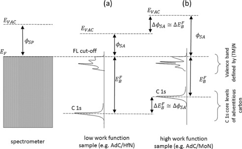
Schematic illustration of the energy level alignment at the interface between adventitious carbon layer and a) the low work function substrate, and b) the high work function substrate. For all tested samples the sum of and is constant, which is indicative of vacuum level alignment.
In conclusion, we established by using a series of TM nitride thin‐film layers covered with a few monolayers of adventitious carbon (AdC), that the BE of the C 1s peak of AdC measured with respect to the Fermi edge depends on the substrate, and varies from 284.08 eV for MoN to 285.52 eV for the HfN sample in the as‐received state. This wide spread in C 1s peak position is independent of the time samples are exposed to ambient atmosphere, hence of the AdC layer thickness. This disturbing result shows that the commonly used referencing of XPS spectra against the C 1s peak of AdC is unreliable. Moreover, we demonstrate that the C 1s signal closely follows the variation of sample work function , such that the sum is constant at 289.50±0.15 eV, indicating alignment to the vacuum level. Thus, the position of the C 1s peak from AdC layer is decoupled from the instrument Fermi level and is steered by the sample work function, and as such cannot be used for reliable BE referencing of XPS spectra. A possible remedy here is a complementary measurement of and referencing to C 1s set at 289.50− , which, as we demonstrate, yields consistent results for the whole series of TM nitrides, irrespective of air exposure time. Conclusions from this work are not limited to nitrides and likely apply to all substrates that exhibit weak interaction towards AdC.
Conflict of interest
The authors declare no conflict of interest.
Supporting information
As a service to our authors and readers, this journal provides supporting information supplied by the authors. Such materials are peer reviewed and may be re‐organized for online delivery, but are not copy‐edited or typeset. Technical support issues arising from supporting information (other than missing files) should be addressed to the authors.
Supplementary
Acknowledgements
The authors most gratefully acknowledge the financial support of the VINN Excellence Center Functional Nanoscale Materials (FunMat) Grant 2005‐02666, the Swedish Government Strategic Research Area in Materials Science on Functional Materials at Linköping University (Faculty Grant SFO‐Mat‐LiU 2009‐00971), the Knut and Alice Wallenberg Foundation Grant 2011.0143, and the Åforsk Foundation Grant 16‐359.
G. Greczynski, L. Hultman, ChemPhysChem 2017, 18, 1507.
References
- 1. Sokolowski E., Nordling C., Siegbahn K., Phys. Rev. 1958, 110, 776. [Google Scholar]
- 2. Hagström S., Nordling C., Siegbahn K., Z. Phys. 1964, 178, 439. [Google Scholar]
- 3. Axelson G., Ericson U., Fahlman A., Hamrin K., Hedman J., Nordberg R., Nordling C., Siegbahn K., Nature 1967, 213, 70. [Google Scholar]
- 4. Nordberg R., Albridge R. G., Bergmark T., Ericson U., Fahlman A., Hamrin K., Hedman J., Johansson G., Nordling C., Siegbahn K., Lindberg B., Nature 1967, 214, 481. [Google Scholar]
- 5. Fahlman A., Hamrin K., Hedman J., Nordberg R., Nordling C., Siegbahn K., Nature 1966, 210, 4. [Google Scholar]
- 6. Siegbahn K., Nordling C., Fahlman A., Nordberg R., Hamrin K., Hedman J., Johansson G., Bergmark T., Karlsson S.-E., Lindgren I., Lindberg B., ESCA—Atomic, Molecule and Solid State Structure Studied by Means of Electron Spectroscopy, Almqvist & Wiksells Boktryckeri, Uppsala, Sweden, 1967. [Google Scholar]
- 7. Metson J. B., Surf. Interface Anal. 1999, 27, 1069. [Google Scholar]
- 8.NIST X-ray Photoelectron Spectroscopy Database, Version 4.1 (National Institute of Standards and Technology, Gaithersburg, 2012), http://srdatA.nist.gov/xps/. Accessed: 2016-11-22.
- 9. Swift P., Surf. Interface Anal. 1982, 4, 47. [Google Scholar]
- 10. Johansson G., Hedman J., Berndtsson A., Klasson M., Nilsson R., J. Electron Spectrosc. Relat. Phenom. 1973, 2, 295. [Google Scholar]
- 11. Kohiki S., Oki K., J. Electron Spectrosc. Relat. Phenom. 1984, 33, 375. [Google Scholar]
- 12. Kinoshita S., Ohta T., Kuroda H., Bull. Chem. Soc. Jpn. 1976, 49, 1149. [Google Scholar]
- 13. Werrett C. R., Bhattacharya A. K., Pyke D. R., Appl. Surf. Sci. 1996, 103, 403. [Google Scholar]
- 14. Gross Th., Ramm M., Sonntag H., Unger W., Weijers H. M., Adem E. H., Surf. Interface Anal. 1992, 18, 59. [Google Scholar]
- 15. Pélisson-Schecker A., Hug H. J., Patscheider J., Surf. Interface Anal. 2012, 44, 29. [Google Scholar]
- 16. Jacquemin M., Genet M. J., Gaigneaux E. M., Debecker D. P., ChemPhysChem 2013, 14, 3618. [DOI] [PubMed] [Google Scholar]
- 17.According to the Scopus Database search for “XPS” and “magnetron sputtering” articles published during 2010–2016, as of 2016-11-24.
- 18. Barr T. L., Seal S., J. Vac. Sci. Technol. A 1995, 13, 1239. [Google Scholar]
- 19. Greczynski G., Mráz S., Hultman L., Schneider J. M., Appl. Surf. Sci. 2016, 385, 356. [Google Scholar]
- 20. Tanuma S., Powell C. J., Penn D. R., Surf. Interface Anal. 2011, 43, 689. [Google Scholar]
- 21. Ishii H., Sugiyama E., Ito E., Seki K., Adv. Mater. 1999, 11, 605. [Google Scholar]
- 22. Hagstrum H. D., Surf. Sci. 1976, 54, 197. [Google Scholar]
- 23. Pireaux J. J., Svensson S., Basilier E., Malmqvist P.-Ä., Gelius U., Caudano R., Siegbahn K., Phys. Rev. A 1976, 14, 2133. [Google Scholar]
- 24. Lögdlund M., Greczynski G., Crispin A., Kugler T., Fahlman M., Salaneck W. R., Photoelectron Spectroscopy of Interfaces for Polymer-Based Electronic Devices, in Conjugated Polymer and Molecular Interfaces: Science and Technology for Photonic and Optoelectronic Application (Eds.: W. R. Salaneck, K. Seki, A. Kahn, J. J. Pireaux), Marcel Dekker, New York, 2001. [Google Scholar]
- 25. Braun S., Salaneck W. R., Fahlman M., Adv. Mater. 2009, 21, 1450. [Google Scholar]
- 26. Rhoderick E. H., Williams R. H., Metal-Semiconductor Contacts, Clarendon Press, Oxford, 1988. [Google Scholar]
- 27. Greczynski G., Hultman L., Appl. Phys. Lett. 2016, 109, 211602. [Google Scholar]
Associated Data
This section collects any data citations, data availability statements, or supplementary materials included in this article.
Supplementary Materials
As a service to our authors and readers, this journal provides supporting information supplied by the authors. Such materials are peer reviewed and may be re‐organized for online delivery, but are not copy‐edited or typeset. Technical support issues arising from supporting information (other than missing files) should be addressed to the authors.
Supplementary


