Abstract
This research communication presents a rapid and facile microwave-assisted synthesis of single crystalline nanosheets (SCNSs) of hexagonal lead iodide (PbI2) decorated with Au nanoparticles, a potential optoelectronics material. Homogeneous low dimensional AuNP decoration in PbI2 resulted in a new absorption band at ~604 nm and a shift in band gap from 3.23 to 3.00 eV. The significant enhancement of photoluminescent (PL) intensity observed in the AuNP-PbI2 SCNSs is attributed to the coupling of the localized surface plasmon resonanzce of AuNP leading to improved excitation and emission rates of PbI2-SCNSs in the region of the localized electromagnetic field. The Au-PbI2 SCNSs display a compelling increment in photoconductivity, and its fabricated photodetector showed a stable and switchable photo-response. Due to ease of synthesis and enhanced photoconductivity along with appealing PL features, Au-PbI2 SCNS has the potential to be used as a material of choice when fabricating an optoelectronic devices of high performance.
Introduction
In the current materials research scenario, the atomically thin nanostructures (i.e., nanosheets) of two (2D) or (3D) dimensional materials with a layered structure such as molybdenum di-sulfide, graphene, boron nitride, transition metal dichalcogenide and nano-semiconductors1–11 gained a lot of attention due to their promising potentials in industrial-technological applications. Nanoscale lead iodide (PbI2), a layered p-type nano semiconductor with a wide band gap of 2.27 eV, is one such important nanostructured material that has been extensively utilized in series of applications including active matrix flat panel imagers, mammography energy range detection, photoconductors, photo-detectors, photovoltaic, sensors, biological labeling and diagnostics, LEDs and PC solar cells, etc.12–16. Layered halide PbI2 exhibits a large number of polytypes17, with PbI2 consists of I-Pb-I repeating units stacked along c-axis and the PbI2 interlayers that are connected by van der Waals forces. Due to the robust Pb lone-pair s orbital and I p orbital anti-bonding connection, PbI2 exhibits ultralow conductivity and high light conversion capability18. Recently, Zhang et al. reported the growth of ultrathin single crystals of the PbI2 materials and studied its photodetector characteristics19. Wei et al. reported its single crystal growth and studied its visible-light photo-detector application20. PbI2 nanostructures have been synthesized using various methodologies21,22. However, the synthesis of PbI2 doped nanosheets using hydrothermal and microwave methods are newly explored23–25. In spite of appreciated opto-electronic properties of PbI2, there is a significant space to improve its optoelectronic features via nanostructuring and doping with plasmonic nanoparticles. Keeping that in view, efforts to fabricate PbI2 nanosheets with the Au dopant as an active and standard plasmonic nanoparticle are urgently required. Nevertheless, accurate nanoengineering of a particularly well-defined morphology of nanostructure is in principle a challenging task and rarely reported for many of the known nanomaterials. The noble metal nanocrystals/nanoparticles like: Gold (Au), Platinum (Pt), and Silver (Ag) are of a captivating class of materials of inimitable chemical and physical possessions that attain countless claims in the field of biosensing, photonics, catalysis etc.1,26–30. Au nanoparticles doping of various synthesized key materials is reported in the literature with remarkable modification in the doped materials properties1,31. Hence, it can be predicted that the Au noble metal nanoparticles (NPs) may anchor on the PbI2 single crystalline nanosheets (SCNSs) and it could possibly extend its functions as an innovative photodetector, photoconductor, optoelectronic and also as a catalytic nanomaterial, which has not been reported on Au doped PbI2 so far, however, reported for many other materials previously22,28,32–35.
Hence, herein, we report a rapid and facile microwave-assisted synthesis of Au nanoparticles (AuNPs) decorated PbI2 SCNSs with uniform hexagonal morphology. The synthesized nanosheets were characterized by the state of the art techniques. The results provide strong evidence of the potential applications of the fabricated AuNPs decorated PbI2 SCNSs and may prove its usefulness in optical and visible-light photodetector device applications and also open a new field of investigation on the titled material for future utilizations.
Materials and Methods
Lead acetate [Pb(C2H3O2)2], sodium iodide (NaI), Cetyl Trimethyl Ammonium Bromide (CTAB), Gold (III) chloride [AuCl3] are taken from Alfa Aesar and Sigma Aldrich Pvt. Ltd. In the first step, 0.5M Pb(C2H3O2)2 was taken in 50 ml distilled water in well gutted cylindrical flask and continuously stirred (700 rpm) at constant temperature ~70 °C until a transparent and homogeneous solution was achieved and named as solution A. A stock solution was prepared for 10 g CTAB as surfactant in 1 liter DD water and 50 ml of it was added to solution A, as surfactant played a significant character in preparation of exact shape nanostructured materials23,36,37. For Au doping, 1 wt% of Gold (III) chloride was added to the solution A. Next, NaI solution obtained by dissolving 1M NaI in 50 ml water was slowly added, and the formation of a deep yellow precipitate was seen. The yellow precipitate confirms the formation of lead iodide (PbI2). For microwave-assisted synthesis, the prepared solution was poured into a cylindrical glass vessel and kept inside a domestic microwave system only for 15 minutes at 700 W, and natural cooling was done. The used domestic microwave system was indigenously modified as shown in Fig. 1 of our previous report25. The final product was washed many times with distilled water during the filtration and finally dried at 100 °C in an oven for 24 h.
Figure 1.
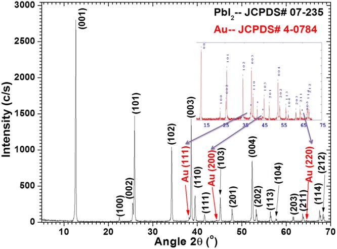
Indexed XRD pattern for Au doped PbI2 nanosheets.
The investigation of the crystalline structure of the synthesized nanosheets is carried out on Shimadzu X-600 Japan powder X-ray diffractometer (CuKα radiation). DXR FT-RAMAN spectrometer was used to measure the spectra in 600–60 cm−1 wavenumber range using 532 nm laser excitation source with only 0.2 mW power. SEM (equipped with EDXS) and TEM is applied on a JSM 6360 and JEOL-EM- 2100 -HR TEM, LA, Japan system to analyze shape, size, spatial spreading of Au NPs and Au doping composition. UV-Visible spectra were documented on a JASCO V-570 UV-Vis-NIR spectrophotometer in 190 to 1000 nm wavelength region. Lumina fluorescence spectrometer was applied to measure photoluminescence (PL) in 350–630 nm range. To study dielectric and alternating current conductivity properties, the capacitance, impedance, and loss tangent measurements were carried out on a KEITHLEY 4200-SCS over a wide frequency range at 300 K. For electrical measurements; the samples were simply designed from prepared doped and undoped PbI2 SCNSs as given in scheme I (see Supplementary Data). For photoconductivity measurements, the sample was fixed on the sample holder for optical cryostat (Oxford optistat DN2). The inner and outer chambers of the cryostat were evacuated to about 10−4 Torr using Edward vacuum system. The desired temperature was achieved using the Oxford temperature controller of model ITC601. The programmable digital electrometer (Keithley 6517b electrometer) used as DC power supply and an ammeter measured the very low current. A tungsten lamp, used for illuminating the sample, was connected to a variac to obtain the desired light intensity. A focusing system consisting of two convex lenses was adjusted between the light source and the sample for obtaining a full and homogeneous illumination on the sample. The experimental arrangement used for the steady-state and transient measurements is shown in Scheme II (see Supplementary Data).
Results and Discussion
X-ray diffraction analysis
XRD examination was performed to inspect the excellence, size, and positioning of synthesized Au doped PbI2 nanosheets. Figure 1 illustrated a measured and indexed XRD pattern of Au doped PbI2 nanosheets. High intensity and sharpness of diffraction peaks confirm good crystallinity of nanosheets and no extra peak due to impurity was seen. The peaks present in the XRD pattern were in agreement with those reported in JCPDS (No. 07–235) for PbI2 and (No. 4–0784) for Au. The XRD pattern display the reflection peaks at 12.674° (001), 22.511° (100), 25.506° (002), 25.915° (101), 34.275° (102), 38.674° (003), 39.519° (110), 41.665° (111), 45.209° (103), 52.399° (004), 53.290° (202), 56.487° (113), 57.726° (104), 61.580° (203), 63.751° (211), 67.569° (114), 68.32° (212) that are corresponding to hexagonal phase of PbI2 nanostructure with 2H Polytypes23,38. Fascinatingly, three additional comparatively low-intensity peaks situated at 38.14°, 44.42°, and 64.6° are allocated to (111), (200) and (220) planes, respectively and are ascribed to FCC structure of Au39,40. The intensity of Au diffraction peaks are less compare to PbI2 and may improved by annealing. The highest intensity was observed along (001) plane which indicates the growth of single crystalline nanosheets along this plane. The estimated lattice parameters were found to be a = b = 4.5593 Å, c = 6.9872 Å and V = 125.783 Å3, which are in agreement with standard PbI2 [JCPDS No. 7–0235].
The average values of grain size (L) and strain (ε) were calculated using well-known relations23 and are found to be 26.760 nm and 1.38 × 10⁻³, respectively. The calculated value of V is enlarged due to doping compared to pure PbI2 nanostructures as reported previously23,24. This can be explicated by Vegard’s law, according to this law when doping incorporation takes place on the substitutional or interstitial position in any material the lattice parameters are found to shrivel or inflate, respectively. Due to the smaller ionic radii of Au3+ (99 pm)41 compared to Pb2+ (119 pm), Au gains more possibility to go into the interstitial sites of PbI2. The enlarged value of V for Au doped PbI2 sample confirms the incorporation of Au in PbI2 matrix.
Vibrational spectroscopy analysis
The Raman modes of pure PbI2 and Au doped PbI2 depicted in Fig. 2 are consistent with 2H polytypes of PbI2 predominantly42,43. The Raman modes are observed at ~72.5, 94.3, 109.5, 165.77, and 214.9 cm−1 for pure PbI2 and at ~70.1, 92.8, 107.8, 164.2, 212.8 cm−1 for Au doped PbI2. The absence of any extra Raman peaks and enhanced intensity confirms the virtuous quality of the prepared product. Raman intensity is found to be remarkably enhanced by Au doping in PbI2. Moreover, the full-width half maxima (FWHM) of the highest intensity peak (~93 ± 1 cm−1) was calculated for the pure and doped PbI2 and found to be ~37.19 and 10.76 cm−1, respectively. Furthermore, the under peak areas of these peaks were also evaluated and found to be 35713 and 38555 for the pure and doped product. This clearly indicates that prepared products possess better crystallinity. Enhancement in intensity of lines specifies that nanosheets are of good crystallinity. Moreover, small shifting in Raman modes of nanosheets (Au doped) compares to nanorods (pure) was also observed. As it is known that 2H-PbI2 has only 3 atoms in one unit cell and hence have 9 degrees of vibrational motions. Predominantly, 2H-PbI2 is expected to have only two bands due to the symmetric stretching A1g band at 97 cm−1 and, doubly degenerated Eg band at 74 cm−1 owing to the shearing motion of two I layers21. These bands in the currently synthesized nanostructures are situated at ~92 ± 3 and 72 ± 2 cm−1, which are slightly shifted due to nano size structures and also due to more relaxed binding. Redshift and expansion of Raman lines authenticate relaxed nanostructure formation which may be owed to relaxed q- vector. More explanation can be found elsewhere about shifting and expansions in Raman lines44–46. It may be mentioned here that no extra peak in the Raman spectrum was observed due to Au doping in PbI2. Such results were also reported for Au decorated MoS2 as well as other doped materials1,47.
Figure 2.
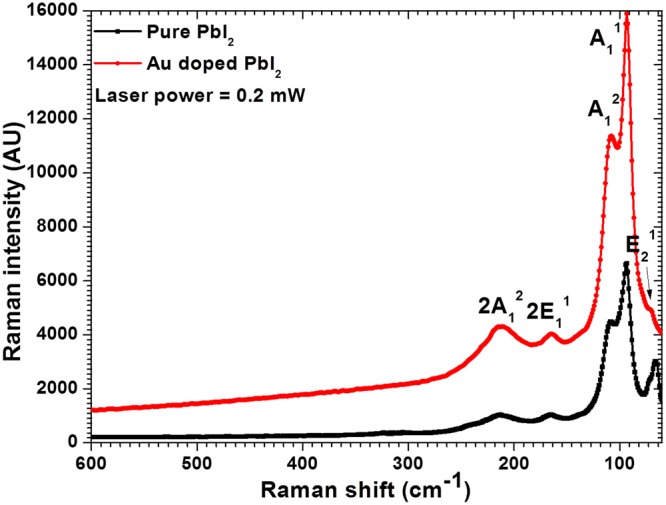
Raman spectra for pure and Au doped PbI2 NRs and NSs.
Elemental composition and morphological analyses
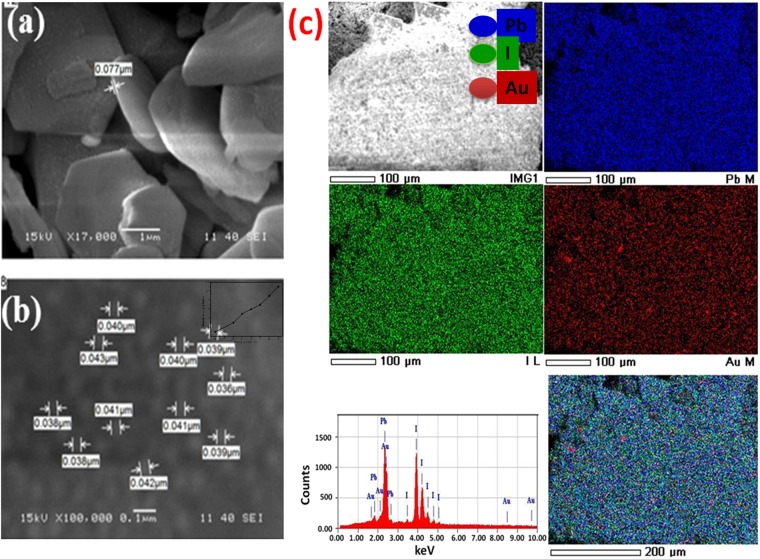
The elemental composition and distribution of Au-PbI2 were studied by EDX and SEM mapping analysis. The recorded SEM micrograph of Au-PbI2 nanosheets is depicted in Fig. 3(a) which exhibit hexagonal shape. These single crystalline nanosheets have thickness <80 nm and their sizes are in µm range. A close observation of a typical nanosheet in Fig. 3(b) reveals an unvarying spreading of Au nanoparticles on PbI2. The average size of Au nanoparticles is less than 40 nm (Histogram is shown in the inset of Fig. 3(b). There is a possibility of error in size as we have measured it manually using SMile View software. Energy dispersive X-ray (EDX) spectroscopy mapping over a representative Au-PbI2 nanosheet in Fig. 3(c) shows a homogeneous distribution of the corresponding Pb, I and Au elements. The EDX spectrum of nanosheet is shown in the left bottom panel. The morphologies of pure and doped PbI2 nanostructures are reported to show nanoparticles, nanocrystals, nanobelts, nanorods, nanosheets, etc. synthesized by different techniques23,24,38,48–50. However, in the present case, the morphology of Au-PbI2 still retains a hexagonal nanosheet structure with uniform Au nanoparticles distribution. These Au doped PbI2 single crystalline nanosheets could offer incomparable optoelectronic properties and can be used in diverse device applications10.
Figure 3.
(a,b) SEM micrographs and (c) SEM mapping of elemental distribution and EDX spectrum of Au doped PbI2 SCNSs.
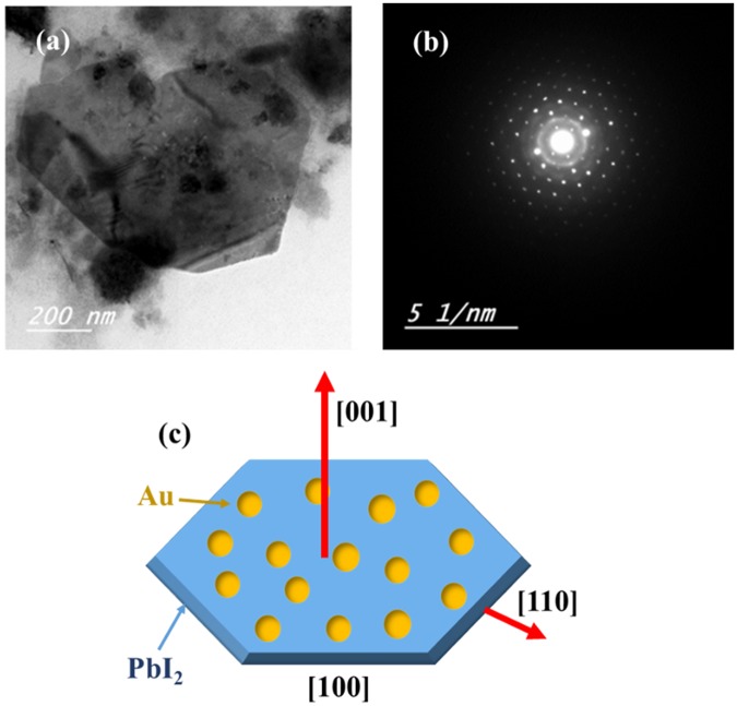
To get further insight into the microstructure of Au-PbI2, high-resolution transmission electron microscopy (HRTEM) study was done. Figure 4(a) shows the HRTEM micrograph of Au-PbI2 nanosheet. The selected area electron diffraction (SAED) pattern in Fig. 4(b) shows the dotted pattern of single crystalline PbI2 and a polycrystalline ring of Au nanoparticles. Clear diffraction spots of the SAED pattern are consistent with high quality and hexagonal structured single crystalline PbI2 nanosheet. Figure 4(c) shows the schematic of the Au-PbI2 nanosheet structure.
Figure 4.
Images of (a) HRTEM, (b) SAED and (c) schematic of Au-PbI2 SCNSs.
Optical studies
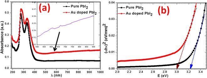
Figure 5(a) showed the measured absorbance spectra at room temperature. From the figure, it can be noticed that the Au doped PbI2 single crystalline nanosheets show more absorbance in the visible light region than the pure PbI2 nanorods with two absorption peaks between 230 nm to 420 nm. The enhancement in the absorption provides clear evidence on AuNPs formation on PbI2 SCNSs which may be seen in the last SEM image while watching it very closely. Moreover, Au doped PbI2 showed two absorption peaks at ~604 and ~665 nm in wavelength range of 500–900 nm (see inset of Fig. 5(a)); these peaks are maybe appeared due to absorption induced by surface plasmon resonance (SPR) that lies at ~630 nm wavelength and for Au nano colloid and Au doped films51–54. Absorbance for pure Au nanoparticles is reported at 525 nm47. It may be mentioned here that the absorbance spectra are recorded in DMF by making the transparent with a light yellow color solution of the prepared nanostructures. SPR is caused by collective oscillations of free electrons in metallic nanoparticles persuaded by exterior electromagnetic radiation, and its spectral features are strongly based on properties of mutual nanoparticles and host matrix53. A clear red shift in absorption edge is observed towards the higher wavelength in the nanosheets compared to nanorods. Two absorption bands are observed in the absorbance data which were used to determine the energy gap through Tauc’s plot achieved by Tauc’s formula and depicts in Fig. 5 (b). As the titled material is a well known direct band gap material so the value of energy gap , is computed from graphs corresponding to joining point, where , of incidental straight line of the curve vs. , at x-axis, where and are known as photon energy and absorption coefficient, respectively. Here, to evaluate the values the Beer-Lambert relation is applied, i.e., , where A is absorbance and t is the width of quartz cuvette (10 mm) used for the measurement. The calculated values of for pure and doped PbI2 are 3.23 eV and 3.00 eV, respectively. Decrease in the band gap of PbI2 is observed due to Au doping, however, band gap values are much larger than bulk value (i.e., 2.27 eV)16. These band gaps are noted to be analogous to recent literature values55,56. Such a reduction in band gap is also reporteda for Au doped TiO2 nanoparticles51. The higher value of band gap may indicate the occurrence of the confinement effect in prepared products. Such a high band gap value of prepared nanostructures makes them suitable for electro-optic devices57–61.
Figure 5.
Examination of (a) absorbance and (b) energy gap for pure and Au doped PbI2.
Photoluminescence (PL) analysis
PL emission spectra recorded for both nanostructures at the excitation wavelength, are shown in Fig. 6. This spectra shows three distinct emission peaks at about 367 (3.380 eV), 430 (2.885 eV) and 535 nm (2.319 eV), however in spectrum of pure these emission peaks are observed at about 368 (3.371 eV) (UV-C or near violet emission) and 467 nm (2.656 eV) (blue emission) and 550 nm (2.256 eV) (green emission). The enhancement in intensity of PL emission is found by Au doping. The emission peaks at 2.656 eV and 2.256 eV are found to be shifted towards the higher energy by 0.229 eV and 0.063 eV in Au doped PbI2 nanosheets. The broad emission peak at 2.256 eV in pure and 2.319 eV in doped is assigned to G band that ascends from recombination of a trapped carrier that may be due to deep imperfection at interior or surface of the nanostructures. This emission peaks may also be assigned to D band which is associated to donar-acceptor pairs. Another broad emission peak at 2.656 eV in pure and 2.885 eV in doped PbI2 is may be attributed to bound excitons (EB), and peaks at 3.371 eV and 3.380 eV in pure and doped PbI2, respectivily, are occurred due to free excitons (EF)55,62,63. All the observed emissions are shifted towards higher energy or lower wavelength.
Figure 6.
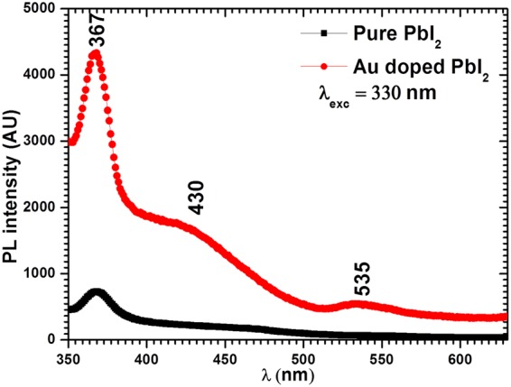
Photoluminescence spectra for pure and Au doped PbI2.
Dielectric and ac electrical conductivity analyses
Dielectric values of constant , loss () and total alternating current electrical conductivity were calculated by measuring the C, Z, and tanδ values of fabricated nanosheets in 3 kHz to 10 MH frequency range. Values of and were calculated using the equation:
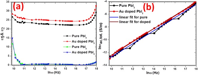
where t is thickness, is vacuum space permittivity and A is area. The calculated values of and over a wide range of frequencies are depicted in Fig. 7(a). The stable values of are obtained in the tested frequency region and that sanctions their application in optoelectronic devices. The value is enriched for Au doped PbI2 (25) nanosheets compared to nanorods of pure PbI2 (22). The attained electrical values in current work are comparable with other reported work in the literature on nano and bulk PbI223,38,64. As we have performed our studies over a high frequency range, the electric field dipole is not obeying the alternating field65–69. The plot shows a same trend as of , the initial decrease in the value of was observed, however at the higher frequency it becomes stable and very low which proves that the prepared nanosheets are low defective. Such nanosheets will be more effective in various applications.
Figure 7.
Examination for (a) ε1 & ε2 and (b) ln σac.tot. of pure and Au doped PbI2.
Moreover, the values were calculated from the equation: and shown in Fig. 7(b) with frequency. The values of was enriched for Au doped PbI2 which indicates better electrical properties that can be more efficient in semiconductor devices. Also the enhancement in the values of was noticed with frequency which means it follows the universal frequency power law. The conduction behavior was analyzed using Jonscher law70, , here, s is a frequency exponent and other symbols have usual meanings. The plot between and has been shown in Fig. 7(b) from which the value of s was obtained through the slope of this plot, and found below 1 for both samples. This means that the value of s is <1, which imply that the behavior of charge carriers is managed by correlated barrier hopping (CBH)56. Generally, for unordered systems, charge carriers progression is mainly deal with two physical actions known as CBH and quantum mechanical tunneling. Though, the exact character of charge transfer might be explicate with temperature disparity of s56.
Electrical properties analysis
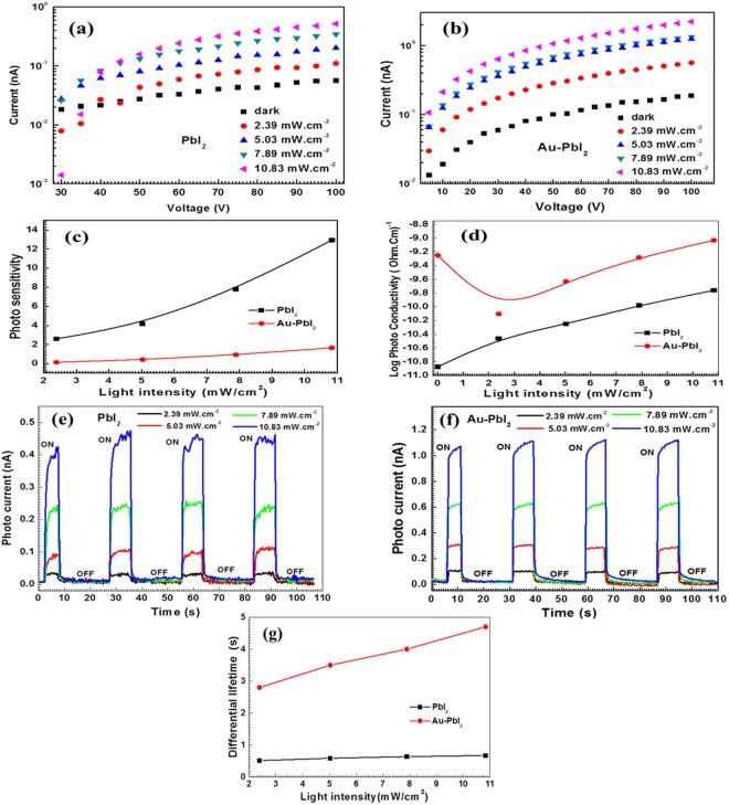
Lead iodide, Lead iodide based and other inorganic perovskites are reported to be good photodetectors20,71–74. Effect of Au doping and annealing on photoswitchability of ZnO is also reported previously75,76. Figure 8(a,b) shows I-V characteristics of PbI2 and Au-PbI2 at different incident light intensities along with the dark current reference. It is seen that the light current increases with incident light intensity. The (dark current) ON/OFF ratio values are (0.056 nA) 9 and (0.187 nA) 12 at 100 V for PbI2 and Au-PbI2, respectively. The light intensity power dependence of photoconductivity in Fig. 8(c) compares the photosensitivity of PbI2 and Au-PbI2 while Fig. 8(d) clearly shows photoconductivity enhancement in Au-PbI2 over PbI2. To investigate the stability of PbI2 nanosheet based photodetectors, the photo-response is measured by turning ON/OFF the light periodically at a constant interval for multiple cycles. In the OFF state of the laser, the photodetector has a low current (~0.01 nA) while the ON state increases the photodetector current rapidly to a saturation value. The low dark current indicates low noise and hence, higher device sensitivity. The switching mechanism can be easily understood in the previous report on Au doped ZnO by Mishra et al.75. The time-resolved photo-responses at various illumination powers are shown in Fig. 8(e,f). The photocurrents displayed no obvious deviations after 120 s, implying the good photodetector stability and reversibility. Also, the ON/OFF switching behavior retains well and is reversible. The differential lifetime [Fig. 8(g)] as a function of light intensity shows an enhancement of a factor of 6 in Au-PbI2 over PbI2. The response time and recovery time are found to be improved in Au-PbI2. From Fig. 8, it clear that Au doped PbI2 nanosheets exhibit better electrical properties than pure PbI2. The currently prepared nanosheets showed comparable electrical properties as reported for ultrathin as well as large PbI2 single crystal19,20.
Figure 8.
Current-voltage characteristics of (a) PbI2 and (b) Au-PbI2 at different incident light intensities, (c) Photosensitivity and (d) Photoconductivity as a function of light intensity, Time-resolved photoresponse of (e) PbI2 and (f) Au-PbI2 at different incident light intensities. (g) Differential lifetimes.
Conclusions
An efficient and rapid microwave-assisted synthesis of hexagonal single crystalline nanosheets of 1 wt% Au doped PbI2 has been described in this research. Structural characterization (XRD, SEM, TEM) revealed the homogenous distribution of polycrystalline Au nanoparticles (~40 nm) decorating PbI2 nanosheets. The vibrational modes are observed to be red-shifted compared to the bulk values of the studied material due to the confinement effects. While absorbance spectra displayed a new band at ~604 nm in doped nanostructures which may be due to the presence of Au. Optical energy gap was reduced from 3.23 eV to 3.00 eV when PbI2 was doped with Au nanoparticles. The intensity of PL emission was enhanced many folds in Au doped PbI2 due to the SPR of Au metal nanoparticle. This results in enhancing the excitation and emission rate of PbI2 nanosheets in the localized electromagnetic field. Dielectric constant value is enriched from 22 to 25, and total ac electrical conductivity was also found to be enhanced in Au doped samples. Au doped PbI2 nanosheets give a better photoconductive response, and the fabricated photodetector from single crystalline nanosheets show promising, stable, switchable photo-response. Such results give a cutting-edge idea in recognition of enhanced photoluminescent, photoconductor and electrical devices fabricated based on the Au-PbI2 single crystalline nanosheets.
Electronic supplementary material
Acknowledgements
The authors would like to express their gratitude to Research Center for Advanced Materials Science-King Khalid University, Saudi Arabia, for support.
Author Contributions
Mohd. Shkir: Have synthesized the final product and written the manuscript. I.S. Yahia: He is has contributed in results and discussion part. V. Ganesh: Has helped in performing dielectric measurements. Yugandhar Bitla: He contributed in analysis and writing of electrical properties, TEM and designing of Fig. 4(c). I.M. Ashraf: has contributed in electrical measurements and their discussion. Ajeet Kaushik: Contributed in overall modification and scientific discussion. S. AlFaify: Has contributed in performing the characterization and analyzing of the final product.
Competing Interests
The authors declare no competing interests.
Footnotes
Publisher's note: Springer Nature remains neutral with regard to jurisdictional claims in published maps and institutional affiliations.
Electronic supplementary material
Supplementary information accompanies this paper at 10.1038/s41598-018-32038-5.
References
- 1.Shi Y, et al. Selective decoration of Au nanoparticles on monolayer MoS2 single crystals. Scientific Reports. 2013;3:1839. doi: 10.1038/srep01839. [DOI] [PMC free article] [PubMed] [Google Scholar]
- 2.Geim AK, Novoselov KS. The rise of graphene. Nature materials. 2007;6:183–191. doi: 10.1038/nmat1849. [DOI] [PubMed] [Google Scholar]
- 3.Novoselov KS, et al. Two-dimensional gas of massless Dirac fermions in graphene. Nature. 2005;438:197–200. doi: 10.1038/nature04233. [DOI] [PubMed] [Google Scholar]
- 4.Kubota Y, Watanabe K, Tsuda O, Taniguchi T. Deep ultraviolet light-emitting hexagonal boron nitride synthesized at atmospheric pressure. Science. 2007;317:932–934. doi: 10.1126/science.1144216. [DOI] [PubMed] [Google Scholar]
- 5.Wang H, et al. Integrated circuits based on bilayer MoS2 transistors. Nano letters. 2012;12:4674–4680. doi: 10.1021/nl302015v. [DOI] [PubMed] [Google Scholar]
- 6.Gao T, Wang T. Two-Dimensional Single Crystal CdS Nanosheets: Synthesis and Properties. Crystal growth & design. 2010;10:4995–5000. doi: 10.1021/cg1010852. [DOI] [Google Scholar]
- 7.Liu J, et al. 2D ZnO mesoporous single-crystal nanosheets with exposed {0001} polar facets for the depollution of cationic dye molecules by highly selective adsorption and photocatalytic decomposition. Applied Catalysis B: Environmental. 2016;181:138–145. doi: 10.1016/j.apcatb.2015.07.054. [DOI] [Google Scholar]
- 8.Wang, F. et al. Nanometre-thick single-crystalline nanosheets grown at the water-air interface. Nature Communications7 (2016). [DOI] [PMC free article] [PubMed]
- 9.Wang Y, et al. Microwave-assisted synthesis of SnO2 nanosheets photoanodes for dye-sensitized solar cells. The Journal of Physical Chemistry C. 2014;118:25931–25938. doi: 10.1021/jp5089146. [DOI] [Google Scholar]
- 10.Liu, Y.-Q. et al. Facile microwave-assisted synthesis of klockmannite CuSe nanosheets and their exceptional electrical properties. Scientific Reports4 (2014). [DOI] [PMC free article] [PubMed]
- 11.Tiginyanu, I. et al. Strong light scattering and broadband (UV to IR) photoabsorption in stretchable 3D hybrid architectures based on Aerographite decorated by ZnO nanocrystallites. Scientific Reports6, 32913, https://www.nature.com/articles/srep32913#supplementary-information10.1038/srep32913 (2016). [DOI] [PMC free article] [PubMed]
- 12.Street R, et al. Comparison of PbI2 and HgI2 for direct detection active matrix x-ray image sensors. Journal of Applied Physics. 2002;91:3345–3355. doi: 10.1063/1.1436298. [DOI] [Google Scholar]
- 13.Shah KS, et al. Lead iodide X-ray detection systems. Nuclear Instruments and Methods in Physics Research Section A: Accelerators, Spectrometers, Detectors and Associated Equipment. 1996;380:266–270. doi: 10.1016/S0168-9002(96)00346-4. [DOI] [Google Scholar]
- 14.Barnakov YA, Ito S, Dmitruk I, Tsunekawa S, Kasuya A. Production and optical study of PbI 2 nanorod-like particles. Scripta Materialia. 2001;45:273–277. doi: 10.1016/S1359-6462(01)01021-1. [DOI] [Google Scholar]
- 15.Mu R, Tung Y, Ueda A, Henderson D. Chemical and size characterization of layered lead iodide quantum dots via optical spectroscopy and atomic force microscopy. The Journal of Physical Chemistry. 1996;100:19927–19932. doi: 10.1021/jp960605a. [DOI] [Google Scholar]
- 16.Zhu X, Wei Z, Jin Y, Xiang A. Growth and characterization of a PbI2 single crystal used for gamma ray detectors. Crystal Research and Technology. 2007;42:456–459. doi: 10.1002/crat.200610847. [DOI] [Google Scholar]
- 17.Verma, A. R. & Krishna, P. Polymorphism and polytypism in crystals. 1966, 341 P. John Wiley and Sons, Inc., 605 Third Avenue, New York, N. Y. 10016 (1965).
- 18.Yin W-J, Shi T, Yan Y. Unusual defect physics in CH3NH3PbI3 perovskite solar cell absorber. Applied Physics Letters. 2014;104:063903. doi: 10.1063/1.4864778. [DOI] [Google Scholar]
- 19.Zhang J, et al. Layered ultrathin PbI2 single crystals for high sensitivity flexible photodetectors. Journal of Materials Chemistry C. 2015;3:4402–4406. doi: 10.1039/C4TC02712D. [DOI] [Google Scholar]
- 20.Wei Q, et al. Large-sized PbI2 single crystal grown by co-solvent method for visible-light photo-detector application. Materials Letters. 2017;193:101–104. doi: 10.1016/j.matlet.2017.01.049. [DOI] [Google Scholar]
- 21.Kasi GK, Dollahon NR, Ahmadi TS. Fabrication and characterization of solid PbI2 nanocrystals. Journal of Physics D: Applied Physics. 2007;40:1778. doi: 10.1088/0022-3727/40/6/026. [DOI] [Google Scholar]
- 22.Shkir M, et al. Facile hydrothermal synthesis and characterization of cesium-doped PbI2 nanostructures for optoelectronic, radiation detection and photocatalytic applications. Journal of Nanoparticle Research. 2017;19:328. doi: 10.1007/s11051-017-4020-6. [DOI] [Google Scholar]
- 23.Shkir M, Yahia IS, Ganesh V, Algarni H, AlFaify S. Facile hydrothermal-assisted synthesis of Gd3+ doped PbI2 nanostructures and their characterization. Materials Letters. 2016;176:135–138. doi: 10.1016/j.matlet.2016.04.062. [DOI] [Google Scholar]
- 24.Shkir M, AlFaify S, Yahia IS, Ganesh V, Shoukry H. Microwave-assisted synthesis of Gd3+ doped PbI2 hierarchical nanostructures for optoelectronic and radiation detection applications. Physica B: Condensed Matter. 2017;508:41–46. doi: 10.1016/j.physb.2016.12.016. [DOI] [Google Scholar]
- 25.Shkir M, AlFaify S. Tailoring the structural, morphological, optical and dielectric properties of lead iodide through Nd3+ doping. Scientific Reports. 2017;7:16091. doi: 10.1038/s41598-017-16086-x. [DOI] [PMC free article] [PubMed] [Google Scholar]
- 26.Dong X, Shi Y, Huang W, Chen P, Li LJ. Electrical detection of DNA hybridization with single‐base specificity using transistors based on CVD‐grown graphene sheets. Advanced Materials. 2010;22:1649–1653. doi: 10.1002/adma.200903645. [DOI] [PubMed] [Google Scholar]
- 27.He S, et al. Graphene-based high-efficiency surface-enhanced Raman scattering-active platform for sensitive and multiplex DNA detection. Analytical chemistry. 2012;84:4622–4627. doi: 10.1021/ac300577d. [DOI] [PubMed] [Google Scholar]
- 28.Huang F, Baumberg JJ. Actively tuned plasmons on elastomerically driven Au nanoparticle dimers. Nano letters. 2010;10:1787–1792. doi: 10.1021/nl1004114. [DOI] [PubMed] [Google Scholar]
- 29.Lu Y-C, et al. Platinum− gold nanoparticles: a highly active bifunctional electrocatalyst for rechargeable lithium− air batteries. Journal of the American Chemical Society. 2010;132:12170–12171. doi: 10.1021/ja1036572. [DOI] [PubMed] [Google Scholar]
- 30.Murdoch M, et al. The effect of gold loading and particle size on photocatalytic hydrogen production from ethanol over Au/TiO 2 nanoparticles. Nature Chemistry. 2011;3:489. doi: 10.1038/nchem.1048. [DOI] [PubMed] [Google Scholar]
- 31.Koo HY, et al. Gold nanoparticle-doped graphene nanosheets: sub-nanosized gold clusters nucleate and grow at the nitrogen-induced defects on graphene surfaces. Journal of Materials Chemistry. 2012;22:7130–7135. doi: 10.1039/c2jm16195h. [DOI] [Google Scholar]
- 32.Jaramillo TF, et al. Identification of active edge sites for electrochemical H2 evolution from MoS2 nanocatalysts. Science. 2007;317:100–102. doi: 10.1126/science.1141483. [DOI] [PubMed] [Google Scholar]
- 33.Monroy E, Omnès F, Calle F. Wide-bandgap semiconductor ultraviolet photodetectors. Semiconductor Science and Technology. 2003;18:R33. doi: 10.1088/0268-1242/18/4/201. [DOI] [Google Scholar]
- 34.Yang S, et al. High-performance few-layer Mo-doped ReSe 2 nanosheet photodetectors. Scientific Reports. 2014;4:5442. doi: 10.1038/srep05442. [DOI] [PMC free article] [PubMed] [Google Scholar]
- 35.Hu P, et al. Highly responsive ultrathin GaS nanosheet photodetectors on rigid and flexible substrates. Nano letters. 2013;13:1649–1654. doi: 10.1021/nl400107k. [DOI] [PubMed] [Google Scholar]
- 36.Zhang Y, Hu L, Zhu T, Xie J, Zhao X. High yield Bi2Te3 single crystal nanosheets with uniform morphology via a solvothermal synthesis. Crystal growth & design. 2013;13:645–651. doi: 10.1021/cg3013156. [DOI] [Google Scholar]
- 37.Fan Z, Huang X, Tan C, Zhang H. Thin metal nanostructures: synthesis, properties and applications. Chemical Science. 2015;6:95–111. doi: 10.1039/C4SC02571G. [DOI] [PMC free article] [PubMed] [Google Scholar]
- 38.Shkir M, Yahia IS, AlFaify S, Abutalib MM, Muhammad S. Facile synthesis of lead iodide nanostructures by microwave irradiation technique and their structural, morphological, photoluminescence and dielectric studies. Journal of Molecular Structure. 2016;1110:83–90. doi: 10.1016/j.molstruc.2016.01.014. [DOI] [Google Scholar]
- 39.Perumal V, et al. ‘Spotted Nanoflowers’: Gold-seeded Zinc Oxide Nanohybrid for Selective Bio-capture. Scientific Reports. 2015;5:12231. doi: 10.1038/srep12231. [DOI] [PMC free article] [PubMed] [Google Scholar]
- 40.Guo J, et al. High-performance gas sensor based on ZnO nanowires functionalized by Au nanoparticles. Sensors and Actuators B: Chemical. 2014;199:339–345. doi: 10.1016/j.snb.2014.04.010. [DOI] [Google Scholar]
- 41.Mandal S, et al. Aerobic oxidation of benzyl alcohol over mesoporous Mn-doped ceria supported Au nanoparticle catalyst. Journal of Molecular Catalysis A: Chemical. 2013;378:47–56. doi: 10.1016/j.molcata.2013.05.011. [DOI] [Google Scholar]
- 42.Sears WM, Klein M, Morrison J. Polytypism and the vibrational properties of Pb I 2. Physical Review B. 1979;19:2305. doi: 10.1103/PhysRevB.19.2305. [DOI] [Google Scholar]
- 43.Wangyang P, Sun H, Zhu X, Yang D, Gao X. Mechanical exfoliation and Raman spectra of ultrathin PbI2 single crystal. Materials Letters. 2016;168:68–71. doi: 10.1016/j.matlet.2016.01.034. [DOI] [Google Scholar]
- 44.Alim KA, Fonoberov VA, Shamsa M, Balandin AA. Micro-Raman investigation of optical phonons in ZnO nanocrystals. Journal of Applied Physics. 2005;97:124313–124313. doi: 10.1063/1.1944222. [DOI] [Google Scholar]
- 45.Milekhin, A. G. et al. In MRS Proceedings. E13. 17 (Cambridge Univ Press) (2002).
- 46.Bhaumik A, Shearin A, Delong R, Wanekaya A, Ghosh K. Probing the Interaction at the Nano–Bio Interface Using Raman Spectroscopy: ZnO Nanoparticles and Adenosine Triphosphate Biomolecules. The Journal of Physical Chemistry C. 2014;118:18631–18639. doi: 10.1021/jp506200a. [DOI] [PMC free article] [PubMed] [Google Scholar]
- 47.Xiang Q, et al. Au nanoparticle modified WO3 nanorods with their enhanced properties for photocatalysis and gas sensing. The Journal of Physical Chemistry C. 2010;114:2049–2055. doi: 10.1021/jp909742d. [DOI] [Google Scholar]
- 48.Sengupta A, Mandal K, Zhang J. Ultrafast electronic relaxation dynamics in layered iodide semiconductors: a comparative study of colloidal BiI3 and PbI2 nanoparticles. The Journal of Physical Chemistry B. 2000;104:9396–9403. doi: 10.1021/jp000980+. [DOI] [Google Scholar]
- 49.Zhu G, et al. Controllable synthesis of PbI2 nanocrystals viaáaásurfactant-assisted hydrothermal route. Applied Physics A. 2010;98:299–304. doi: 10.1007/s00339-009-5412-y. [DOI] [Google Scholar]
- 50.Ma D, et al. A facile hydrothermal synthesis route to single-crystalline lead iodide nanobelts and nanobelt bundles. Journal of nanoscience and nanotechnology. 2005;5:810–813. doi: 10.1166/jnn.2005.142. [DOI] [PubMed] [Google Scholar]
- 51.Rahulan KM, Ganesan S, Aruna P. Synthesis and optical limiting studies of Au-doped TiO2 nanoparticles. Advances in Natural Sciences: Nanoscience and Nanotechnology. 2011;2:025012. [Google Scholar]
- 52.Torrell M, et al. Nanoscale color control of TiO 2 films with embedded Au nanoparticles. Materials Letters. 2010;64:2624–2626. doi: 10.1016/j.matlet.2010.08.031. [DOI] [Google Scholar]
- 53.Torrell M, et al. Tuning of the surface plasmon resonance in TiO2/Au thin films grown by magnetron sputtering: the effect of thermal annealing. Journal of Applied Physics. 2011;109:074310. doi: 10.1063/1.3565066. [DOI] [Google Scholar]
- 54.Lee M, Chae L, Lee KC. Microstructure and surface plasmon absorption of sol-gel-prepared Au nanoclusters in TiO 2 thin films. Nanostructured Materials. 1999;11:195–201. doi: 10.1016/S0965-9773(99)00032-X. [DOI] [Google Scholar]
- 55.Kaviyarasu K, Sajan D, Selvakumar MS, Augustine Thomas S, Prem Anand D. A facile hydrothermal route to synthesize novel PbI2 nanorods. Journal of Physics and Chemistry of Solids. 2012;73:1396–1400. doi: 10.1016/j.jpcs.2012.06.005. [DOI] [Google Scholar]
- 56.Chakrabarty N, Mukherjee A, Sinha S, Basu S, Meikap A. Observation of correlated barrier hopping in blue luminescent PbI 2 nanoparticles. Physica E: Low-dimensional Systems and Nanostructures. 2014;64:134–140. doi: 10.1016/j.physe.2014.06.022. [DOI] [Google Scholar]
- 57.Shakir M, Kushwaha S, Maurya K, Bhagavannarayana G, Wahab M. Characterization of ZnSe nanoparticles synthesized by microwave heating process. Solid State Communications. 2009;149:2047–2049. doi: 10.1016/j.ssc.2009.08.021. [DOI] [Google Scholar]
- 58.Shkir M, et al. Synthesis of ZnTe Nanoparticles by Microwave Irradiation Technique, and Their Characterization. Nanoscience and Nanotechnology Letters. 2012;4:405–408. doi: 10.1166/nnl.2012.1328. [DOI] [Google Scholar]
- 59.Kirschman, R. K. High temperature electronics. (IEEE Press New York, NY, 1999).
- 60.Casady J, Johnson RW. Status of silicon carbide (SiC) as a wide-bandgap semiconductor for high-temperature applications: A review. Solid-State Electronics. 1996;39:1409–1422. doi: 10.1016/0038-1101(96)00045-7. [DOI] [Google Scholar]
- 61.Chow TP, Tyagi R. Wide bandgap compound semiconductors for superior high-voltage unipolar power devices. Electron Devices, IEEE Transactions on. 1994;41:1481–1483. doi: 10.1109/16.297751. [DOI] [Google Scholar]
- 62.Bol A, Meijerink A. Long-lived Mn 2+ emission in nanocrystalline Z n S: M n 2+ Physical Review B. 1998;58:R15997. doi: 10.1103/PhysRevB.58.R15997. [DOI] [Google Scholar]
- 63.Yang P, Mengkai Lii YD, XüDuolong GZ. Photoluminescence properties of ZnS nanoparticles co-doped with Pb2þ and Cu2þ. J Chem Phys Lett. 2001;336:76–80. doi: 10.1016/S0009-2614(01)00038-0. [DOI] [Google Scholar]
- 64.Dugan A, Henisch H. Dielectric properties and index of refraction of lead iodide single crystals. Journal of Physics and Chemistry of Solids. 1967;28:971–976. doi: 10.1016/0022-3697(67)90213-2. [DOI] [Google Scholar]
- 65.Batra A, Carmichael‐Owens C, Simmons M, Aggarwal M, Lal R. Design of a solution crystal growth crystallizer with a versatile electronic reciprocal motion control for a crystals holder. Crystal Research and Technology. 2005;40:757–760. doi: 10.1002/crat.200410425. [DOI] [Google Scholar]
- 66.Hill, N. E. Dielectric properties and molecular behaviour. (Van Nostrand Reinhold, 1969).
- 67.Shakir M, et al. Enhancement of second harmonic generation, optical and dielectric properties in L-asparagine monohydrate single crystals due to an improvement in crystalline perfection by annealing. Journal of Applied Crystallography. 2010;43:491–497. doi: 10.1107/S0021889810008745. [DOI] [Google Scholar]
- 68.Shakir M, Kushwaha S, Maurya K, Arora M, Bhagavannarayana G. Growth and characterization of glycine picrate—Remarkable second-harmonic generation in centrosymmetric crystal. Journal of crystal growth. 2009;311:3871–3875. doi: 10.1016/j.jcrysgro.2009.06.007. [DOI] [Google Scholar]
- 69.Shakir M, et al. Dielectric behaviour and ac electrical conductivity analysis of ZnSe chalcogenide nanoparticles. Chalcogenide Letters. 2009;6:655–660. [Google Scholar]
- 70.Jonscher AK. Theuniversal’dielectric response. Nature. 1977;267:673–679. doi: 10.1038/267673a0. [DOI] [Google Scholar]
- 71.Cao F, et al. Highly stable and flexible photodetector arrays based on low dimensional CsPbBr 3 microcrystals and on-paper pencil-drawn electrodes. Journal of Materials Chemistry C. 2017;5:7441–7445. doi: 10.1039/C7TC02108A. [DOI] [Google Scholar]
- 72.Yu D, et al. Dimensionality and interface engineering of 2d homologous perovskites for boosted charge-carrier transport and photodetection performances. The Journal of Physical Chemistry Letters. 2017;8:2565–2572. doi: 10.1021/acs.jpclett.7b00993. [DOI] [PubMed] [Google Scholar]
- 73.Mousa AM, Jamil SS, Ponpon JP. Effect of Doping and Post Annealing on PbI2 Photoconductivity. Journal of Materials Science and Engineering. 2012;2:215–219. [Google Scholar]
- 74.Liu X, et al. Low‐Voltage Photodetectors with High Responsivity Based on Solution‐Processed Micrometer‐Scale All‐Inorganic Perovskite Nanoplatelets. Small. 2017;13:1700364. doi: 10.1002/smll.201700364. [DOI] [PubMed] [Google Scholar]
- 75.Mishra Y, et al. Crystal growth behaviour in Au-ZnO nanocomposite under different annealing environments and photoswitchability. Journal of Applied Physics. 2012;112:064308. doi: 10.1063/1.4752469. [DOI] [Google Scholar]
- 76.Mishra, Y. K. & Adelung, R. ZnO tetrapod materials for functional applications. Materials Today (2017).
Associated Data
This section collects any data citations, data availability statements, or supplementary materials included in this article.


