Abstract
Metallic and dielectric nanoparticles (NPs) have synergistic electromagnetic properties but their positioning into morphologically defined hybrid arrays with novel optical properties still poses significant challenges. A template-guided self-assembly strategy is introduced for the positioning of metallic and dielectric NPs at pre-defined lattice sites. The chemical assembly approach facilitates the fabrication of clusters of metallic NPs with interparticle separations of only a few nanometers in a landscape of dielectric NPs positioned hundreds of nanometers apart. This approach is used to generate two-dimensional interdigitated arrays of 250 nm diameter TiO2 NPs and clusters of electromagnetically strongly coupled 60 nm Au NPs. The morphologydependent near- and far-field responses of the resulting multiscale optoplasmonic arrays are analyzed in detail. Elastic and inelastic scattering spectroscopy in combination with electromagnetic simulations reveal that optoplasmonic arrays sustain delocalized photonic–plasmonic modes that achieve a cascaded E-field enhancement in the gap junctions of the Au NP clusters and simultaneously increase the E-field intensity throughout the entire array.
1. Introduction
Two-dimensional (2D) arrays of dielectric nanoparticles (NPs) achieve a regular corrugation of the refractive index and, thus, represent 2D photonic crystals (PCs) that allow for a rational tuning of photonic band-gaps, [1,2] an efficient guiding of light, [3] and a deceleration of the group velocity of light [4] through variation of the PC morphology. The light localization properties of dielectric PCs, and thus the ability to generate high local E-field intensities are, however, limited by diffraction. The use of noble metal NPs as building blocks in 2D metal NP arrays offers (in principle) a viable strategy to overcome this limitation. Resonant charge density oscillations, so called localized surface plasmon resonances (LSPRs), can induce an oscillating charge build-up on the surface of the noble metal NPs and a strong localization of electromagnetic fields in deeply subdiffraction limit volumes within the evanescent field of the NPs. Metal NPs re-radiate part of the incident light and, consequently, Au and Ag NPs or NP clusters arranged into arrays with periodic [5–10] or deterministic aperiodic [11–13] morphology efficiently diffract the incident light. Depending on the morphology of the array and the angle of incidence, light of a given wavelength λ is either diffracted into radiating modes or into evanescent modes that propagate along the surface. For specific array geometries the light diffracted into the array plane can resonantly couple to LSPR modes of the NPs to form photonic-plasmonic hybrid modes. [10,14–21] These geometric resonances are associated with sharp spectral features, [22] an electromagnetic field enhancement [16] and an increase in local density of optical states (LDOS). [14]
While for interparticle separations on the order of the wavelength of light the electromagnetic interactions between individual NPs in the array are limited to diffractive coupling, at shorter interparticle separations, , where k0 and λ0 are the free space wavenumber and wavelength, respectively, a hybridization [23] of plasmon modes becomes possible. Strong quasi-static near-field interactions between individual NPs result in this case in a dramatic increase in E-field localization. [24] If clusters of strongly coupled NPs are arranged into extended arrays, the availability of both short- and long-range coupling mechanisms provide additional opportunities for generating a cascaded multiscale E-field enhancement. [15] The feasibility of this concept has been validated in regular arrays of AuNP clusters (NCAs) [5] in which the E-field provided by individual clusters is further enhanced by delocalized array modes that couple to the strongly localized cluster modes. [5,7,8,25] Despite the appeal for realizing high E-field enhancements in discrete plasmonic structures and extended metal NP arrays, high dissipative losses in metals at optical frequencies set ultimate limits for trapping, storing and guiding the light in metallic structures. These functionalities remain, therefore, largely the domain of dielectric PCs.
There has recently been significant interest in mitigating the respective limitations of photonic and plasmonic materials outlined above by combining both components into metallo-dielectric—or optoplasmonic—hybrid structures. [26–36] The integration of plasmonic gap antennas into an array of dielectric NPs that generates a landscape of dielectric photonic modes is especially appealing since it promises additional degrees of freedom for tailoring the electromagnetic coupling in the array in both spatial and frequency domain. [27,28,37,38] The practical realization of hybrid arrays with defined optical resonances remains, however, challenging since it requires a high level of control for simultaneously positioning both metallic and dielectric NPs. We demonstrate in this manuscript that template-guided self-assembly strategies represent a facile strategy for addressing this fabrication problem. We assemble hybrid arrays that contain TiO2 NPs and clusters of electromagnetically strongly coupled Au NPs at pre-defined lattice sites and investigate the electromagnetic coupling mechanisms that determine the optical near- and far-field responses of these novel electromagnetic materials in detail. Since the spectral range of interest in this work lies below 2.4 eV and, thus, below the band gap of amorphous TiO2, we treat the metal oxide as a dielectric with a constant refractive index of nr = 1.8. [39]
2. Results and Discussion
2.1. Template-Guided Self Assembly of Optoplasmonic NCAs
Template guided self-assembly strategies [5,40–43] have two key fabrication steps: the definition of assembly sites through a lithographically fabrication technique (e.g. electron beam lithography, EBL) and the subsequent assembly of colloidal NPs onto the lithographically defined assembly sites. While EBL makes it possible to define the separation, Λ, between individual assembly sites on length scales ranging from ~10 nm to hundreds of nanometers and beyond, the self-assembly step facilitates the creation of clusters of close-packed NPs with interparticle separations of a few nanometers or below. Due to its versatility in creating gap structures over such a broad range, template guided self-assembly is a convenient method for generating multiscale NP arrays. [5,7,15] Another – underutilized – advantage of template-guided self-assembly strategies is that the diameter (D) and shape of the assembly sites provide some control over the size of the NPs assembled on that site. [7] We took advantage of this structural control parameter to program the morphology of optoplasmonic arrays that contain individual TiO2 NPs and clusters of 60 nm Au NPs on separate lattice sites.
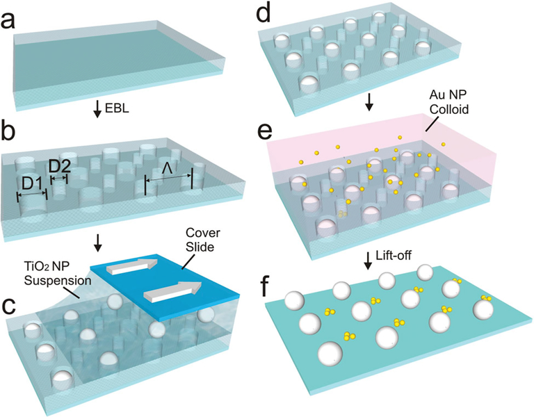
Our assembly strategy is schematically illustrated in Figure 1. In the first step, a lithographically defined template with two different assembly site diameters D2 < D1 is generated. This template is exposed to dielectric particles with an average particle diameter d1, D2 < d1 < D1, which can only bind to the assembly sites with diameter D1. In a subsequent second assembly step, noble metal NPs with a diameter d2, d2 < D2, are then targeted to the vacant D2 array sites. If the ratio of NP and assembly site diameter, (d2/ D2), is chosen appropriately, the assembly sites can accommodate multiple NPs. The latter facilitates a controlled formation of NP clusters. In this study we exclusively used d1 ≈ 250 nm TiO2 NPs and d2 ≈ 60 nm Au NPs. The assembly site diameters for our optoplasmonic arrays were chosen as D1 ≈ 140 nm and D2 ≈ 270 nm. The d2/ D2 ratio was intended to favor the formation of clusters with ~ 4 NPs since it was shown before that in self-assembled 2D NP clusters with random configuration the E-field enhancement reaches it maximum for cluster sizes n ≈ 4. [5,15] The center-to-center separation between adjacent D1 or D2 binding sitesis defined as Λ in all investigated arrays. In the fabricated hybrid arrays the Λ values for the TiO2N P and Au NP cluster sub-arrays were identical.
Figure 1.
Schematic overview of template-guided self-assembly of optoplasmonic arrays. a) A regular pattern of wells with diameters D1 and D2 (D1 > D2) is created through EBL in a PMMA layer to generate b) a regular mask of assembly sites with two different diameters. The center-to-center separation in the D1 and D2 sub-arrays is Λ. c) Dragging of a suspension of TiO2 NPs with diameters too large to bind to D 2 across the surface results d) in an immobilization of TiO2 NPs onto D1 sites. e) Smaller AuNPs are assembled onto vacant D2 binding sites from a colloidal solution. f) After PMMA lift-off, the final optoplasmonic array is released.
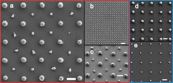
Figure 2 shows scanning electron microscopy (SEM) images of different array types accessible with the template guided self-assembly process. A magnified sections of an optoplasmonic array is shown in (a), a complete array is shown in (b). The sideview in (c) further illustrates the positioning of discrete AuNP clusters between individual TiO2 NPs. The images in (d) and (e) contain top views of a TiO2 NP array and a conventional Au NCA, respectively. Λ was 1000 nm in (a–e). The SEM images in Figure 2 confirm that both TiO2 and Au NPs can be successfully assembled into regular hybrid arrays. Although the D1 assembly sites in the optoplasmonic array show some contamination with additional stacked TiO2 NPs or metal NPs on top of TiO2 NPs under our not-yet optimized assembly conditions, the SEM images in (a-c) overall confirm that the different assembly site diameters indeed preferentially guide the TiO2 and Au NPs to separate lattice sites. We obtained highly regular array geometries in which the TiO2 NPs are located on the vertices of regular squares, each containing a central Au NP cluster. The average number of Au NPs on the D2 sites was 6.2 ± 1.2, and thus acceptably close to the design target. In the following we refer to the size of the optoplasmonic arrays by the i × j TiO2 assembly sites in the array.
Figure 2.
SEM images of 2D arrays generated through template guided self-assembly of d1 = 250 nm TiO2 NPs and d2 = 60 nm Au NPs. a) Magnified section of an optoplasmonic array. b) Complete optoplasmonic array with 20×20 TiO2 NPs. c) Side-view (30° tilt angle) of optoplasmonic array section. d) Section of TiO2 NP array. e) Section of Au NP cluster array (NCA). Λ is 1000 nm in (a) – (e). Scale bars are and 500 nm in (a), (c–e) and 2 μm in (b).
2.2. Far-Field Characterization of Optoplasmonic Arrays
As a first step towards unraveling the multiscale electromagnetic interactions that determine the spectral properties of optoplasmonic arrays in the near- and far-field, we analyzed the elastic scattering spectra of the hybrid arrays as well as of their Au NCA and TiO2 NP sub-arrays. To that end, we fabricated multiple arrays on identical chips with Λ in the range between 700–1000 nm in steps of 100 nm. The fabricated arrays contained 20×20 Au NP clusters, 20×20 TiO2 NPs, or all of these particles combined in case of the hybrid structure. We chose Λ in the range 700–1000 nm, as we anticipated the strongest coupling between photonic and plasmonic modes to occur for grating periods that are close to the plasmon resonance of the individual Au NP clusters. The latter was determined as λplas ≈ 760 nm (Figure S1).
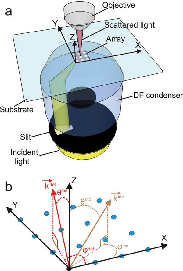
A systematic scheme of the experimental set-up used for the spectroscopic characterization of the fabricated arrays under oblique illumination is shown in Figure 3. The fabricated arrays were illuminated with unpolarized white light through an oil darkfield condenser with a numerical aperture (NA) of 1.2–1.4, corresponding to a range of the incident angle of θinc = 52–68°. We limited the incident wave vectors () with a variable slit in the entrance port (see Experimental Section) and detected the light scattered normal to the array plane through a 10× air objective with a NA of 0.25. For additional details regarding the data acquisition and processing, please refer to the Experimental Section.
Figure 3.
a) Experimental set-up for elastic scattering spectroscopy. The sample is illuminated through a darkfield (DF) condenser whose back aperture is partially blocked. b) Definition of incident () and detected scattered () wave vector and angles and φdet, θinc, and φinc. The position of NPs in the array plane are indicated as blue dots.
The regular 2D NP arrays investigated in this work represent in a first approximation optical gratings, [3,9,20] whose diffraction polar angle for a specific wavelength λ depends on the grating orders m and n, the array periods along the x-,y-axes (Λx and Λy), the incident polar angle 2inc, and the azimuth angles φinc, φdet for incidence and detection, respectively. With a set of 1-dimensional Laue equations [44]
| 1 |
| 2 |
where and are the detection angles along the x- and y- direction, the detection angle for a grating order (m,n) in the 2-dimensional array is obtained for φdet = 0° as:
| 3 |
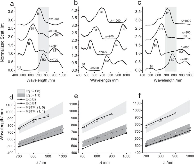
As we will show in the following, the recorded spectra (Figure 4) of all three investigated array types are dominated by two radiating diffraction modes, which can be assigned using Equation (3). We start our analysis with the Au NCAs plotted in Figure 4a. The fitted peak wavelengths of the bands marked as B1 and B2 together with the predicted wavelength range of the (1,1) and (1,0) grating orders are summarized in (Figure 4 d). The theoretical predictions are based on the evaluation of Equation (3) with azimuthal angles of φinc = 0 for the (1,0) mode and φinc = π/ 4 for the (1,1) mode. Furthermore, we assumed that the collecting microscope objective is located in infinity (= 0°) and we used an effective refractive index of nr = 1.24 as average between glass substratum and air superstratum. The linear red-shifts of the fitted peak wavelengths of B1 and B2 as function of Λ are in very good agreement with the theoretical predictions and confirm that these spectral features arise from photonic grating modes. In addition to the grating modes, the Au NCA spectra also contain a spectral feature in the range between 690–830 nm (vertical grey-shaded areas in Figures 4 a and c), which we assign to the plasmon resonance of Au NP clusters on the D2 assembly sites (see Figure S1). While for Λ = 700 nm the (1,0) grating mode and plasmon scattering band spectrally coincide, in all other spectra the plasmon band is identifiable as a shoulder or separate peak near λplas ≈ 760 nm.
Figure 4.
Elastic scattering spectra of a) Au NCA, b) TiO2 NP array and c) optoplasmonichybrid array. The spectra were recorded for arrays with periodicities of Λ = 700 nm, 800 nm, 900 nm, and 1000 nm. All spectra contain the diffractive grating orders (1, 0) (B2) and (1,1) (B1). In a) and c) the shaded areas mark the spectral position of the plasmon resonance in individual Au NP clusters (λplas ≈ 760 nm). The fitted peak wavelengths (Exp) of B1 and B2, the spectral range Equation (3) for (1,1) and (1,0) grating orders for NA = 1.2–1.4 according to Equation (3), and MSTM simulated spectral positions (MSTM) for an incident angle of θinc = 60° (φinc = 45° and 0° for (1,1) and (1,0) mode, respectively) and nr = 1.24 as function of Λ are summarized in d) for Au NCAs, in e) for TiO2 NP arrays, and in f) for optoplasmonic hybrid arrays.
The spectra and fitted peak wavelengths for TiO2 NP arrays are summarized in Figures 4b and e. As observed before for the Au NCAs, the spectra contain again a set of bands B1 and B2 whose spectral position shifts linearly with Λ. Although the experimental values of B1 lie slightly below the range predicted by Equation (3), the agreement is still very good, given the complexity of the experimental system. Differences in the effective refractive index of the effective array plane, the size mismatch between the TiO2 and Au NPs (d1 > d2), as well as experimental variations in the grating period can all contribute to the observed discrepancies.
The spectral data of the optoplasmonic arrays are shown in Figures 4c and f. In this case the fitted peak positions of B1 and B2 are again in excellent agreement with the predictions for the (1,1) and (1,0) diffraction bands according to Equation (3). As observed for the conventional Au NCAs, the spectra in Figure 4 c also contain a distinct feature that arises from the NP cluster plasmon resonance. Interestingly, both Au NCAs and optoplasmonic hybrid arrays have lower relative intensities in the spectral range > 760 nm when compared with the all-dielectric TiO2 NP array. Direct excitation of plasmons as well as photonic-plasmonic mode coupling can achieve a localization of the optical energy in the form of gap plasmons in the NP clusters. This energy redistribution, together with the unavoidable dissipative losses in metals, can account for the reduction in diffracted optical power in this spectral range.
The excellent agreement between recorded and predicted spectral positions according to Equation (3) confirms a high structural integrity for all three assembled array types. The recorded far-field data also provide a superb testbed for the calibration of electromagnetic multiple sphere T-Matrix (MSTM) simulations (see Experimental Section for details). The spectral positions of the simulated (1,0), (1,1) grating orders in model arrays comprising 8 × 8 Au NP clusters, 8 × 8 TiO2 NPs, or both TiO2 NPs and Au NP clusters for polar angles ϕinc = 0° and 45°, respectively, are included in Figure 4 d –f. Some exemplary simulated full spectra are provided in Figure S2 together with the spectral assignments. The close concordance between experimental and MSTM-simulated data in Figure 4d–f confirms that the method accurately describes the far-field spectral response of the arrays under investigation.
2.3. Near-Field Characterization of Optoplasmonic Arrays
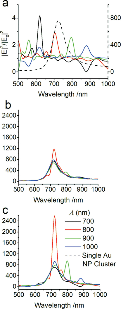
In the next step we applied the calibrated MSTM method to map the interactions of the individual components of the photonic-plasmonic hybrid arrays in the near-field. To that end, we first calculated the near-field spectra at the hottest spots in arrays comprising 20×20 TiO2 NPs, 20×20 Au NP clusters, and optoplasmonic hybrid arrays of 20×20 TiO2 NPs and the corresponding number of Au NP clusters as function of Λ. All near-field spectra were calculated for a plane wave with normal incidence since this corresponds most closely to the experimental SERS measurements we performed (see below). We performed these calculations for triangular NP clusters that had one base oriented parallel to the incident E-field for polarization pointing either in the x-direction or rotated by π /4. Since both of these simulations provided essentially identical trends and peak E -field enhancements, we focus our discussion in the following on the x-polarized incident light. The obtained near-field spectra are summarized in Figure 5. The E-field enhancement for the all-dielectric TiO2 NP array in Figure 5a shows discrete resonances, whose spectral positions red-shift with increasing Λ. The E -field enhancements in the dielectric arrays are much lower than those observed for Au NCAs (Figure 5b). For the latter the near-field spectra are dominated by the cluster plasmon resonance with a simulated peak wavelength of ~ 720 nm. The near-field intensity spectrum for an individual Au NP trimer is included for comparison in Figure 5a. Interestingly, the combination of TiO2 NPs and Au NP clusters in optoplasmonic arrays (Figure 5c) achieves a further significant boost of the near-field intensities beyond what can be obtained in the NCAs at the wavelengths corresponding to the photonic resonances in the TiO2 NP array. Light incident on optoplasmonic arrays normal to the surface is efficiently re-radiated into the array plane by the TiO2 NPs, with the exact wavelength of the re-radiated light depending on the periodicity of the diffractively coupled NPs. If the re-radiated light overlaps with the plasmon resonance of the NP clusters, it is efficiently localized through excitation of LSPRs in the NP clusters. According to the MSTM simulations the near-field maxima of the photonic array modes and the LSPRs overlap in optoplasmonic arrays with Λ ≈ 800 nm. In this geometry photonic-plasmonic mode coupling facilitates a cascaded enhancement of the E-fi eld intensity provided by the individual clusters.
Figure 5.
M STM-simulated E-field intensity enhancement spectra at the hottest electromagnetic spot in a) an array of 20×20 TiO2 NPs; b) a 20 × 20 Au NCA; and c) the combined optoplasmonic array for different Λ values. The near-field intensity spectrum for an individual NP trimer is included in (a) for comparison. Please note the different E-field intensity scales in (a). The E-field intensities of the photonic modes (solid lines) are plotted to the left scale; the E-field intensity of the NP cluster (dashed line) is plotted to the right scale.
We point out that Au NCAs by themselves act as a grating and that photonic-plasmonic mode formation also modulates the E- field enhancement in these arrays. [15] Indeed, the E -field intensity in Au NCAs is predicted to be Λ -dependent as well and to achieve its maximum value for Λ = 800 nm (Figure 5b). The MSTM simulations show, however, clearly that the combination of dielectric and metallic NPs in the optoplasmonic array (Figure 5c) generates a higher peak E -field enhancement than the NCAs. The peak enhancement of the optoplasmonic arrays is by a factor of 2 higher than that of the NCAs: ≈ 2500 vs. ≈ 1250. We attribute this gain in the optoplasmonic arrays to a more efficient in-plane concentration of the incident light through the TiO2 NP sub-array.
We mention in passing that the exact value of the E-field intensity increases with array size. We systematically evaluated the E -field intensity in the three investigated array types as function of array size (Figure S3) and found that the peak E -field intensity grows faster in optoplasmonic than in conventional plasmonic arrays and converges at array sizes of approximately 20 × 20 TiO2 NPs.
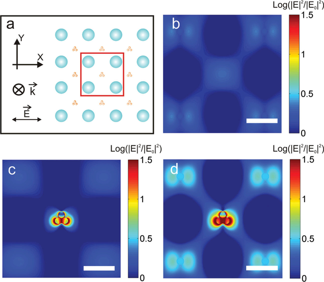
The synergistic interplay between metallic and dielectric array components is further illustrated in Figure 6, which contains maps of the simulated E-field intensity enhancement distributions in the dielectric, plasmonic, and optoplasmonic arrays with Λ = 800 nm at λ = 720 nm. Consistent with a constructive interference of in-plane radiated light that results in the formation of delocalized photonic modes, the TiO2 NP array (Figure 6b) shows increased E-field intensity not only in the direct vicinity of the dielectric NPs but also in the interstitial spaces between the NPs. The E -field enhancement is much weaker than in the case of the Au NCA in Figure 6c, where the electromagnetic energy is strongly focused into the junctions between the NP clusters. This enhancement is further amplifi ed if the Au NP clusters are positioned into the focal points of enhanced E-field intensity of the TiO2 NP sub-array (Figure 6d), where the Au LSPRs can be excited by the focused E-field provided by the dielectric array. Photonic-plasmonic mode [27,33] formation results in this case in an increased E -field enhancement not only around the Au NP clusters but—albeit to a lesser degree—also in the vicinity of the TiO2 NPs and throughout the array. Both the increase in peak E -field intensity as well as the increase in accessible volume with enhanced E-field intensity is anticipated to translate into an overall performance advantage of the optoplasmonic array as substrate for surface enhanced Raman spectroscopy (SERS).
Figure 6.
a) Simulation geometry for the optoplasmonic array. Although only the center area (red box, Au NP plane) is plotted in the near-field map, the whole array is considered in the simulations. Near-field intensity enhancement, |E|2/|E0|2, maps for b) an array of 20×20 TiO2 NPs, c) a 20×20 Au NCA, and d) the corresponding optoplasmonic array at λ = 720 nm. The combination of metallic and dielectric NPs in (d) boosts the near-field intensity not only in the hot-spots defined by the NP clusters but also at locations in the array that are not in the direct vicinity of a NP cluster. All scale bars are 500 nm.
2.4. Validation of Λ -Dependent E-field Intensity Enhancement in Optoplasmonic Arrays Through SERS
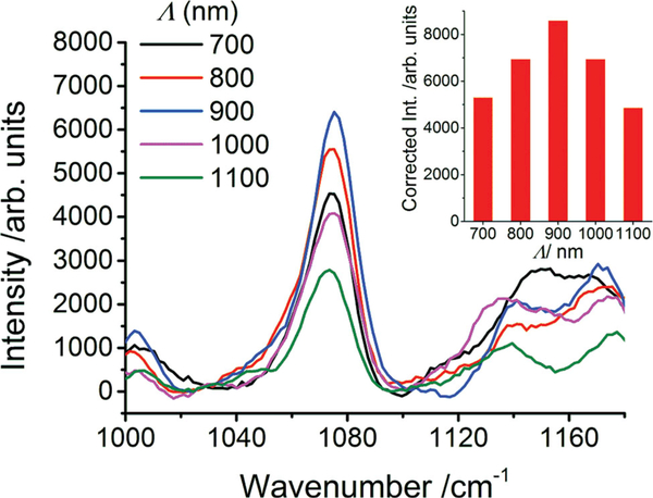
We measured the area-averaged SERS spectra of the small test molecule para-mercaptoaniline (pMA) chemisorbed onto optoplasmonic arrays with array periods between Λ = 700–1100 nm. The entire sample was excited with a 785 nm diode laser in epiillumination configuration, and we collected the signal from a central strip of 4 μm width, as defined by the opening slit of the spectrometer, across the entire array. In Figure 7 we plot the background corrected spectra in the spectral range 980– 1140 cm −1 that contains the C-S stretch mode at 1077 cm -1. The peak intensity of this vibrational transition exhibits a nonlinear dependence of the SERS signal intensity on Λ. The SERS signal intensity initially increases with growing Λ and peaks for Λ = 900 nm. If Λ is further increased, the SERS signal decreases again. Both the spectral position of the photonic-plasmonic resonances and the filling fraction (i.e. NPs per area) depend on Λ. We accounted for this effect by calculating filling fraction corrected intensities, included as inset. The SERS signal intensity maximum remains at Λ = 900 nm after correction for the different number of clusters in the active area.
Figure 7.
SERS spectra of para-mercaptoaniline (pMA) in the range 980–1140 cm −1 obtained on optoplasmonic arrays with different Λ values. The inset shows the filling-fraction corrected intensities of the 1077 cm −1 C–S stretch mode as function of Λ.
SERS signal intensities scale as the product of the E field intensities at the pump and Raman scattering wavelengths. [45,46] Consequently, the observed Λ-dependence of the SERS signal intensity in Figure 7 confirms an additional enhancement of the E-field intensity in the array plane due to geometry-dependent photonic–plasmonic mode coupling. Although the experimentally determined optimum Λ value is somewhat longer than the predicted value (900 vs. 800 nm), this discrepancy is consistent with the shift between the experimentally observed and simulated plasmon resonance wavelengths (780 vs. 720 nm). The origin of the differences between simulations and experiments are attributed to the necessary simplifications in the theoretical model (effective homogenous ambient refractive index, ideal geometries, etc.).
3. Conclusions
Dielectric and metallic NPs have synergistic electromagnetic properties, but the realization of optoplasmonic hetero-nanoparticle arrays with novel properties requires new fabrication approaches that provide precise control over the location of the individual building blocks. We have demonstrated in this manuscript that template guided self-assembly can address this important nanofabrication need since the technique achieves a precise positioning of both colloidal metal and dielectric NPs at separate pre-defined lattice sites. Provided that the assembly site to NP diameter ratio is adequately chosen, the self-assembly technique can also generate clusters of electromagnetically strongly coupled Au NPs. We took advantage of this versatility to integrate Au NP clusters into a regular landscape of TiO2 NPs. We generated hetero-nanoparticles arrays that sustain simultaneous electromagnetic interactions on multiple length scales. The few nanometer gap separations within the Au NP clusters give rise to strong direct near-field coupling, whereas the TiO2 NPs and NP clusters with separations of a few hundreds of nanometers are diffractively coupled. Photonic and plasmonic modes in the array efficiently couple when the photonic modes provided by the TiO2 NP array overlap resonantly with the LSPRs of the Au NP clusters. This coupling further amplifies the E-field enhancement provided by the Au NP clusters and simultaneously increases the E-field enhancement in the space between the NPs throughout the array.
The ability to combine NPs of different composition in one array provides additional degrees of free-om for a rational tuning of the complex multiscale electromagnetic interactions in both spatial and frequency domain, as well for controlling the phase landscape [38] that are missing in conventional plasmonic and dielectric arrays. Optoplasmonic arrays offer, therefore, many opportunities for overcoming the limitations of conventional metallic or dielectric arrays in applications that require increased E-field intensities, tailored near- and far field spectra, and/or tunable emission directionality in areas as diverse as biosensing, information processing, cryptography, and photovoltaics.
4. Experimental Section
Template Preparation A:
300 nm thin poly(methyl methacrylate) (PMMA, molecular weight 950,000 Da, 6% in anisole) was spincoated on top of 1×1 cm glass slides (cleaned by piranha solution for 30 min). The substrates were subsequently soft-baked at 170 °C for 15 min and then sputtered with a 10 nm gold film (Figure 1a). Periodic arrays of wells with diameters (D1 = 270 nm and D2 = 140 nm) and separation, Λ, were then patterned through EBL with a SUPRA 40VP SEM equipped with Raith beam blanker and a nanopattern generation system (NPGS). To optimize the binding efficiency, a dynamic ramp of the electron dosage was applied. After chemical etching of the Au film (7s with the etchant Au Etch Type TFA, Transene Co. Inc.) and development in methyl isobutyle ketone (MIBK): Isopropanol = 1:3 solution, regular arrays of wells were obtained as shown in Figure 1b.
Template Guided Self-Assembly of (Opto)plasmonic Arrays:
Carboxylic acid functionalized spherical TiO2 NPs (~2 50 nm diameter, Corpuscular Inc.) were cleaned through centrifugation and resuspension in DI water twice and finally dispersed to a concentration of 1.6 × 10 11 NPs/mL. The substrate was treated with short plasma cleaning (3 s, 716 V DC, 10 mA DC, 7.16 w, Harrick Plasma) to raise the hydrophility of its surface. The TiO2 suspension was then pipetted onto the well template and sandwiched between the substrate supported template and a glass cover slide using a 500 μ m spacer. The cover slide was translocated across the substrate with a rate of ~5 mm/sec, effectively dragging the TiO2 solution-air interface across the template substrate (Figure 1c). Excessive TiO2 NPs on the PMMA surface were removed via low adhesion tape (Ultratape. #1310). The NP binding process was repeated 2 times. In the next step, the arrays were incubated with L-polylysine (molecular weight 15 000 ~3 0 000 Da, 1% in water) for 30 min (Figure 1d). The arrays were subsequently washed with DI water. In parallel, 0.5 mL of a commercial citrate stabilized 60 nm Au colloid (British Biocell International) were incubated with 2.5 μL of a 10 mM thiol-EG 7 -propionate (EG = ethylene glycol) for 4 h at room temperature. After that, the Au NP colloid was washed by centrifugation and resuspension (2 times) in 30 μL 10 mM phosphate buffer (pH = 8.6) containing 40 m M NaCl. The buffered Au NP colloid was pipetted onto the patterned area of the glass slide and incubated for 40 min (Figure 1e). Excess Au NP colloid was then removed by washing with DI water. After drying in air, the array was contacted with low adhesive tape (Ultratape #1310) to remove NPs bound to the PMMA surface. Finally the PMMA liftoff was performed with 1-methyl-2-pyrrolidinone, releasing the optoplasmonic array after rinsing with acetone (Figure 1f). The assembly process of TiO2 NP arrays or Au NCAs followed similar procedures but all steps related to the immobilization of the other NP species were omitted.
Darkfield Spectroscopy:
The samples were illuminated through an oil dark field condenser (NA = 1.2 ~1.4). The entrance plane of the condenser was covered with a non-transparent disk which had an opening slit (3 × 6 mm) on one side, to define the illumination angle φinc An air objective with NA = 0.25 was used for signal collection. The spectra were collected through a spectrometer (Andor SR303i) equipped with a CCD camera (Andor DU401-BR-DD). The original spectra were corrected by background subtraction from an adjacent area on the chip and normalized by the excitation profile of the light source.
MSTM Simulations:
All computations were performed usingthe multiple sphere T-matrix code developed by D. W. Mackowski. [47] We used the Au dielectric function from Johnson and Christy [48] and assumed a constant refractive index nr = 1.8 for TiO2 NPs. For the ambient medium an effective refractive index of nr = 1.24 was used. In the far-field simulations, the incident angle was set to θinc = 60° for both (1,1) and (1,0) modes, and φinc = 45°and 0° for (1,1) and (1,0) modes, respectively. The scattering angles were θdet = 0° and φdet = 0°. Near field simulations were performed for normal incidence onto the array plane. The Au NP clusters were modeled as trimers with 4 nm edge-to-edge gap. The base of the regular trimers wasparallel to the x-axis. The step size for E-field intensity profile was 2nm.
SERS Measurement:
All samples were first treated with an oxygen plasma cleaning (300 sccm, 300 w, 10 min). After an incubation in 10 mM para-mercaptoaniline (in ethanol) for 12 h, the substrates were then rinsed with copious amount of ethanol and dried in a nitrogen flow. The samples were excited via a diode laser (λ= 785 nm). The total power in the sample plane was 46.5 mW. A 40× air objective (NA = 0.65) was used for SERS signal collection with an acquisition time of 10 s. The SERS spectra were background- and baseline-corrected and the peak height of the 1170 cm -1 peak was determined as the maximum intensity of a Lorentzian fi t.
Supplementary Material
Acknowledgements
This work was supported by the National Science Foundation through grants 1159552, 0853798, 0953121 and by the National Institutes of Health (NIH/NCI) through grant 5R01CA138509.
Footnotes
Supporting Information
Supporting Information is available from the Wiley Online Library or from the author.
References
- [1].Wen F, David S, Checoury X, ElKurdi M, Boucaud P, Opt. Express 2008, 16, 12278. [DOI] [PubMed] [Google Scholar]
- [2].Kao CY, Osher S, Yablonovitch E, Appl. Phys. B 2005, 81, 235. [Google Scholar]
- [3].Mekis A, Chen JC, Kurland I, Fan S, Villeneuve PR, Joannopoulos JD, Phys. Rev. Lett 1996, 77, 3787. [DOI] [PubMed] [Google Scholar]
- [4].Soljacic M, Johnson SG, Fan S, Ibanescu M, Ippen E, Joannopoulos JD, J. Opt. Soc. Am. B 2002, 19, 2052. [Google Scholar]
- [5].Yan B, Thubagere A, Premasiri WR, Ziegler LD, Dal Negro L, Reinhard BM, ACS Nano 2009, 3, 1190. [DOI] [PubMed] [Google Scholar]
- [6].García-Cámara B, Moreno F, González F, Martin OJF, Opt. Express 2010, 18, 10001. [DOI] [PubMed] [Google Scholar]
- [7].Yang L, Yan B, Premasiri WR, Ziegler LD, Negro LD, Reinhard BM, Adv. Funct. Mater 2010, 20, 2619. [Google Scholar]
- [8].Wang J, Yang L, Boriskina S, Yan B, Reinhard BM, Anal. Chem 2011, 83, 2243. [DOI] [PubMed] [Google Scholar]
- [9].Lamprecht B, Schider G, Lechner RT, Ditlbacher H, Krenn JR, Leitner A, Aussenegg FR, Phys. Rev. Lett 2000, 84, 4721. [DOI] [PubMed] [Google Scholar]
- [10].Alaeian H, Dionne JA, Opt. Express 2012, 20, 15781. [DOI] [PubMed] [Google Scholar]
- [11].Gopinath A, Boriskina SV, Feng N-N, Reinhard BM, Negro LD, Nano Lett. 2008, 8, 2423. [DOI] [PubMed] [Google Scholar]
- [12].Dallapiccola R, Gopinath A, Stellacci F, Dal Negro L, Opt. Express 2008, 16, 5544. [DOI] [PubMed] [Google Scholar]
- [13].Poddubny AN, Phys. Rev. B 2011, 83, 075106. [Google Scholar]
- [14].Vecchi G, Giannini V, Gómez Rivas J, Phys. Rev. Lett 2009, 102, 146807. [DOI] [PubMed] [Google Scholar]
- [15].Yan B, Boriskina SV, Reinhard BM, J. Phys. Chem. C 2011, 115, 24437. [DOI] [PMC free article] [PubMed] [Google Scholar]
- [16].Zou S, Schatz GC, J. Chem. Phys 2004, 121, 12606. [DOI] [PubMed] [Google Scholar]
- [17].Auguié B, Barnes WL, Phys. Rev. Lett 2008, 101, 143902. [DOI] [PubMed] [Google Scholar]
- [18].Nikitin AG, Kabashin AV, Dallaporta H, Opt. Express 2012, 20, 27941. [DOI] [PubMed] [Google Scholar]
- [19].García de Abajo FJ, Rev. Mod. Phys 2007, 79, 1267. [Google Scholar]
- [20].Felidj N, Laurent G, Aubard J, Levi G, Hohenau A, Krenn JR, Aussenegg FR, J. Chem. Phys 2005, 123, 221103. [DOI] [PubMed] [Google Scholar]
- [21].Felidj N, Aubard J, Levi G, Krenn JR, Hohenau A, Schider G, Leitner A, Aussenegg FR, Appl. Phys. Lett 2003, 82, 3095. [Google Scholar]
- [22].Hicks EM, Zou S, Schatz GC, Spears KG, Van Duyne RP, Gunnarsson L, Rindzevicius T, Kasemo B, Käll M, Nano Lett. 2005, 5, 1065. [DOI] [PubMed] [Google Scholar]
- [23].Nordlander P, Oubre C, Prodan E, Li K, Stockman MI, Nano Lett. 2004, 4, 899. [Google Scholar]
- [24].Halas NJ, Lal S, Chang W-S, Link S, Nordlander P, Chem. Rev 2011, 111, 3913. [DOI] [PubMed] [Google Scholar]
- [25].Zhou W, Odom TW, Nat Nano 2011, 6, 423. [DOI] [PubMed] [Google Scholar]
- [26].Devilez A, Stout B, Bonod N, ACS Nano 2010, 4, 3390. [DOI] [PubMed] [Google Scholar]
- [27].Barth M, Schietinger S, Fischer S, Becker J, Nüsse N, Aichele T, Löchel B, Sönnichsen C, Benson O, Nano Lett. 2010, 10, 891. [DOI] [PubMed] [Google Scholar]
- [28].Ahn W, Boriskina SV, Hong Y, Reinhard BM, ACS Nano 2012, 6, 951. [DOI] [PubMed] [Google Scholar]
- [29].Yang X, Ishikawa A, Yin X, Zhang X, ACS Nano 2011, 5, 2831. [DOI] [PubMed] [Google Scholar]
- [30].Galisteo-López JF, López-García M, Blanco A, López C, Langmuir 2012, 28, 9174. [DOI] [PubMed] [Google Scholar]
- [31].Galisteo-Lopez JF, Lopez-Garcia M, Lopez C, Garcia-Martin A, Appl. Phys. Lett. 2011, 99, 083302. [Google Scholar]
- [32].Romanov SG, Korovin AV, Regensburger A, Peschel U, Adv. Mater 2011, 23, 2515. [DOI] [PubMed] [Google Scholar]
- [33].Mukherjee I, Hajisalem G, Gordon R, Opt. Express 2011, 19, 22462. [DOI] [PubMed] [Google Scholar]
- [34].Ahn W, Hong Y, Boriskina SV, Reinhard BM, ACS Nano 2013, 7, 4470. [DOI] [PubMed] [Google Scholar]
- [35].Benson O, Nature 2011, 480, 193. [DOI] [PubMed] [Google Scholar]
- [36].Tanemura T, Balram KC, Ly-Gagnon D-S, Wahl P, White JS, Brongersma ML, Miller DAB, Nano Lett. 2011, 11, 2693. [DOI] [PubMed] [Google Scholar]
- [37].Hong Y, Pourmand M, Boriskina SV, Reinhard BM, Adv. Mater 2012, 25, 115. [DOI] [PubMed] [Google Scholar]
- [38].Boriskina SV, Reinhard BM, Opt. Express 2011, 19, 22305. [DOI] [PMC free article] [PubMed] [Google Scholar]
- [39].Umebayashi T, Yamaki T, Itoh H, Asai K, Appl. Phys. Lett 2002, 81, 454. [Google Scholar]
- [40].Liu S, Maoz R, Sagiv J, Nano Lett. 2004, 4, 845. [Google Scholar]
- [41].Cui Y, Björk MT, Liddle JA, Sönnichsen C, Boussert B, Alivisatos AP, Nano Lett. 2004, 4, 1093. [Google Scholar]
- [42].Xia Y, Yin Y, Lu Y, McLellan J, Adv. Funct. Mater 2003, 13, 907. [Google Scholar]
- [43].Lalander CH, Zheng Y, Dhuey S, Cabrini S, Bach U, ACS Nano 2010, 4, 6153. [DOI] [PubMed] [Google Scholar]
- [44].Omar MA, Elementary solid statephysics: principlesandapplications, Addison-Wesley Publishing Company, Boston, Massachusetts, USA: 1975. [Google Scholar]
- [45].Le Ru EC, Etchegoin PG, Chem. Phys. Lett 2006, 423, 63. [Google Scholar]
- [46].Lee SJ, Guan Z, Xu H, Moskovits M, J. Phys. Chem. C 2007, 111, 17985. [Google Scholar]
- [47].Mackowski DW, Mishchenko MI, J. Opt. Soc. Am. A 1996, 13, 2266 [Google Scholar]
- [48].Johnson PB, Christy RW, Phys. Rev. B 1972, 6, 4370. [Google Scholar]
Associated Data
This section collects any data citations, data availability statements, or supplementary materials included in this article.


