Abstract
Spectrally controlled diffusion and reflection of light are key operations for light management in many optical devices. Integration of this operation in complex nanophotonic devices requires a 2D interface that provides tailored spectrum and directivity control. Here, we present a metagrating superstructure that realizes a resonant light reflector with tailored angular scattering profile. Millimeter-sized metasurfaces are built from arrays of combined supercells of 20–50 μm, composed of 5–7 differently pitched metagratings that tailor at will and with large efficiency the angular response. Each supercell is composed of one or more Si Mie resonators, arranged in a periodic array above an Ag back plane and tailored to resonantly scatter light at 650 nm into only the ±1 diffraction orders with very high efficiency. By varying the pitch and supercell design, we can tailor the overall metasurface reflection profile with large flexibility, realizing a broad-angle Lambertian-type scattering metasurface, as well as a large-angle (35–75°) scattering metasurface, both with resonant optical scattering efficiencies above 70%. These ultrathin structures, fabricated using thin-film deposition, electron beam lithography, and reactive ion etching, can find applications for light trapping and spectrum splitting in solar cells and other devices.
Keywords: spectrum and angle control, metagrating, dielectric nanoparticles, Mie resonances, Lambertian scattering
Materials to control light diffusion are traditionally composed of randomly packed high-index particles that support multiwavelength scattering. These materials are typically based on multiple random scattering events and therefore need to have thicknesses much larger than the optical wavelength. The properties of random media used for light scattering in solar cells,1,2 random lasing3,4 and investigation of Anderson localization5,6 have been intensively studied. Random media often used in these studies consist of various types of “white paint”.1−3 Artificially made random media for light diffusion such as photonic glass4 and Mie glass7 have also been demonstrated.
For various applications, it is important to have randomly scattering devices with a much smaller thickness. In recent years, the metasurface literature has offered different solutions for flat two-dimensional surfaces providing diffuse scattering. So far, these solutions have been based on phase-coded metasurfaces, engineered by distributing a limited number of inclusions in a random-like fashion to locally manipulate the phase, amplitude, and polarization of light and thereby the shape of the scattered wavefront. Some work has been done on phase-coded metasurfaces for diffuse-like scattering with quasi-random phase coding in the microwave and infrared regime.8−10 Metasurface diffusers at optical wavelengths were also studied, and their far-field response and performance for speckle-free imaging was studied.11−13 However, graded metasurfaces composed of passive scattering surfaces have a fundamentally limited beam bending efficiency.14−16
In this work, we demonstrate efficient broad-angle and large-angle light scattering from metagratings formed by locally periodic arrays of carefully tailored inclusions above a reflecting backplane, applying and extending a rigorous analytical theory that was introduced by Ra’di et al.17 In the optical spectral range, a metagrating is composed of resonantly scattering plasmonic or Mie particles placed in a periodic array above a metal reflector, supporting a discrete set of grating orders. For a well-chosen scattering cross section and spacing between scatterers and reflector, the specular reflection at resonance is fully canceled by destructive interference of reflection from the back mirror and the zeroth order Floquet scattering mode.17 In addition, the resonant scatterer geometry can be designed to only allow scattering power in one desired diffraction order and to completely suppress scattering into all other allowed orders. Metagratings can be designed to operate around a resonant wavelength, with a tailored angular scattering profile, and an efficiency that is fundamentally limited only by absorption in the involved materials.17 They can operate using either magnetic17 or electric resonant modes.18 Freeform inverse designs and fully analytical schemes to design metagratings employing diffraction gratings have been investigated.19−21 This concept has also been employed to tailor wavefront control in transmission and reflection22−24 using optimized scatterers with a shaped emission profile, without a direct link with theory.
Here, we design a metasurface that combines multiple metagratings with different periodicities placed side by side in a supercell to create a reflector with a precisely engineered scattering profile. We extend the metagrating theory17 and use numerical optimization to create a design based on magnetic Mie modes, experimentally demonstrating the functionality of the combined metagratings. A key feature of the proposed metasurface design is that it relies on a well-defined and precisely engineered scattering profile, in contrast to most random light scattering geometries based on multiple scattering.
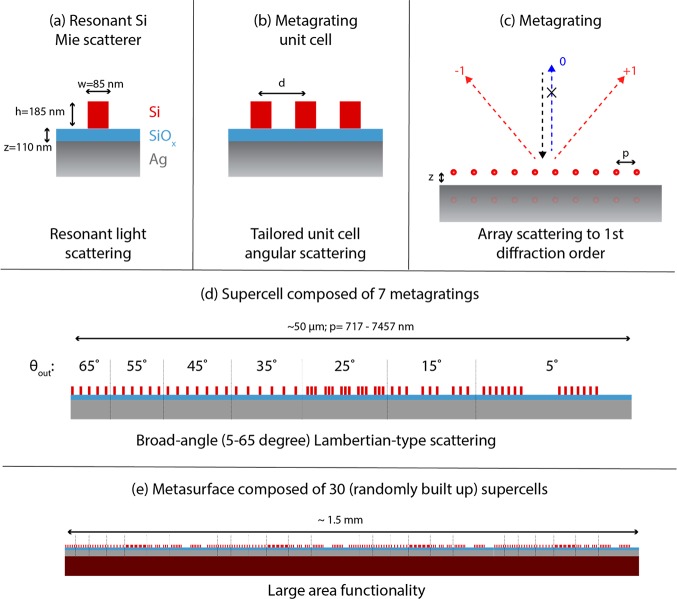
The reflecting metasurface presented here is composed of five characteristic length scales, designed based on the following steps (see Figure 1): (a) Si nanoparticles are designed to have a magnetic Mie resonance in the red spectral range; (b) the unit cells are composed of one or, in part of the structure, multiple scatterers to tailor angular scattering; (c) these unit cells are then placed in periodic arrays above a Ag backplane to form a metagrating that scatters light to a single diffraction order; (d) multiple metagratings are arranged into a supercell composed of seven differently pitched metagratings to create a supercell with tailored angular scattering distribution; (e) a full-scale metasurface sample is then built up from randomly placed supercells.
Figure 1.
Metasurface design and length scales. Unit cells composed of one or more Si Mie resonators are arranged in a periodic array placed above a metal back plane to form a metagrating that scatters into only the ±1 diffraction orders. A supercell of metagratings creates a tailored angular response, and an array of supercells forms the large-area macroscopic metasurface.
Resonant broad-angle scattering profiles with well-defined angular distribution can find applications as diffusors, approaching a Lambertian scatterer. For example, resonant diffusers can enable the creation of a mat appearance effectively creating “nanostructured paint”, which has applications in, e.g., colored solar cells.25,26 Creating structural color using dielectric nanoparticles27−29 has been demonstrated before, focusing on spectral control rather than spectral and directivity control. To demonstrate the versatility of the metagrating design, we also demonstrate a functional surface with tailored large-angle scattering profile. This structure overcomes the typical inefficiencies faced by structures designed to scatter energy toward very large angles and can improve light trapping and spectrum splitting in (tandem) solar cells.
Theory and Design
Following the work of Ra’di et al.,17 we first design a metagrating composed of an array of horizontally oriented magnetic dipoles located at a distance h above a perfect electrical conductor [see schematic in Figure 2(a)]. Here, we consider normally incident light and set the periodicity in order to support two symmetric diffraction orders (i.e., ±1). The distance h can be controlled so that the fields in the specular direction are fully canceled by destructive interference of light reflected from the mirror and the resonantly scattered zeroth-order Floquet grating mode. In this geometry, all light can be redirected to a single desired diffraction order (+1 or −1) by choosing the resonant scatterer geometry in such a way that scattering into the other diffraction order is nullified. Here since we aim at a symmetric angular scattering profile, we will design the metagrating to equally scatter into symmetrically directed +1 and −1 channels.
Figure 2.
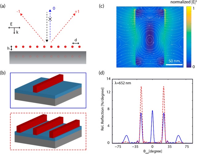
Magnetic dipole resonances in a 1D metagrating array. (a) Periodic array of magnetic dipoles arranged over a ground plane. (b) Schematic of unit cells with one or three silicon bars on a silica spacer layer on top of a silver mirror. (c) Normalized electric field intensity |E|2 and electric field lines (gray) in vertical crosscuts through an 85 nm wide and 180 nm tall Si bar on a 110 nm SiOx spacer layer on top of a silver mirror, parallel to the electric driving field. (d) Simulated angular scattering at λ = 652 nm in the far field for a finite metagrating with just 5 periods with pitch of 1538 nm. Unit cells are composed of a single silicon bar (solid blue line) or three silicon bars (spaced by 230 nm; dashed red line) placed above a Ag ground plane with a 110 nm silica spacer. Light coupling to the specular reflection and second order diffraction is suppressed for the three-particle unit cell.
Throughout the Article, we limit
the calculation and experiments
to 2D functionality under normal incidence; however, the same concepts
can be readily extended to 3D and to any incoming illumination angle.
The magnetic dipoles, induced by the incoming transverse magnetic
(TM) plane wave  with amplitude E0 and free-space wavenumber k0, form a
magnetic current
  where ω
is the angular frequency,
  is the local magnetic
field at the location
of the particle, sum of the incident field, and the reaction from
the array, and αm is the effective magnetic polarizability,
including the array coupling. As shown earlier17 (see also the analytical derivation in the Supporting Information), αm satisfies
the generalized passivity condition
| 1 |
with η0 being the
free-space
wave impedance, d the periodicity in the y direction, and θn the
diffraction angle(s) given by the grating equation. For normal-incident
light, the zeroth order Floquet mode of the radiated field is  , where
  . The direct
reflection from the ground
plane can be canceled by the Floquet mode if
  . This
leads to the following condition:
| 2 |
For a grating with ±1 grating orders, eqs 1 and 2 lead to the design equation for the cancellation of specular reflection:
| 3 |
Next, we create a metasurface that is composed by a distribution of metagratings, each designed to create a symmetric scattering profile over a different angular range. Given the limited size, each of them does not offer large directivity, but this is not an issue since the overall goal is to tailor the scattering over a broad angular range. By combining several of them placed next to each other, the overall scattering distribution can be tailored with large flexibility. In our design, we choose angles in a step size of 10°, to fill a major part of the scattering profile while maintaining the lateral dimension of the metasurface supercell below 100 μm.
Broad-Angle Scattering Metasurface
Numerical Simulations
Two-dimensional finite-difference time domain (FDTD) simulations were performed to design a broad-angle scattering metasurface with engineered scattering profile. The unit cells in each metagrating are composed of one or more silicon rods placed on top of a silver mirror with a silica spacing layer, surrounded by air, see Figure 2(b). Each Si rod has a width of 85 nm and a height of 180 nm, and the silica spacing layer has a thickness of 110 nm. The parameters of the rod are kept constant in all parts of the structure as the performance does not improve substantially for the different metagratings with changing parameters. Details of the numerical optimization can be found in the Supporting Information. The structure is excited by TM-polarized light at normal incidence. The normalized electrical field distribution for a single scatterer on the silica-covered silver mirror at the resonance wavelength λ = 665 nm is plotted in Figure 2(c), and the field lines show the typical electrical field loop corresponding to a magnetic dipole.30 A single supercell of the structure is composed of an array of metagratings that are each composed of 2 to 7 periodically placed unit cells, to steer light efficiently toward the desired angular range. The number of unit cells for each metagrating is indicated in the schematic of Figure 1(c), and the dimensions of all parameters are listed in Table 1. Side-by-side metagratings are spaced by the distance of one of the periodicities. We aim the broad-angle metasurface to operate in the 0–65° angular range, with metagratings scattering from 5 to 65°. The scattering toward 0° is provided by the residual of the specular reflection, so no extra supercells are needed to cover this portion of the scattering spectrum.
Table 1. Overview of Design Parameters for Broad-Angle and Large-Angle Metasurfaces.
| parameter | symbol | broad-angle metasurface | large-angle metasurface |
|---|---|---|---|
| Si Mie scatterer width | w | 85 nm | 85 nm |
| Si Mie scatterer height | z | 180 nm | 180 nm |
| silica spacer layer thickness | t | 110 nm | 110 nm |
| spacing between Mie scatterers and Ag mirror | h | 200 nm | 200 nm |
| number of Mie resonators/spacing in unit cell | n/d | 6/230 nm (5°) | 1 |
| 3/470 nm (15°) | |||
| 3/550 nm (25°) | |||
| 1 (>25°) | |||
| grating pitch in metasurface | p | 720 nm (65°) to 7500 nm (5°) | 670 nm (75°) to 1130 nm (35°) |
| number of metagratings in supercell | 5 | 7 | |
| size of supercell | 50 μm | 20 μm | |
| spacing between supercells | 720 to 7500 nm | 670 to 1130 nm | |
| total metasurface size | 1.5 × 1.5 mm2 | 1.5 × 1.5 mm2 |
To address angles below 30°, we could utilize conventional gradient metasurfaces that perform well for small angles.14 Here, instead, to cover this angular range we extend the metagrating concept and design a surface that not only eliminates scattering into the specular direction but also has zero scatterings into higher order modes other than ±1, leaving only scattering into the first diffraction orders (i.e., ±1). To do so, we compose the metagrating unit cell (that needs a single scatterer in the case of large-angle deflection, as in the design described above) of either 3 or 6 identical scatterers, with their lateral distance tuned to achieve a scattering angular distribution that mainly couples to the first-order diffraction angle. This new approach has two advantages compared to conventional gradient metasurfaces: first, by maintaining the symmetry in the unit cell, the scattering effect remains angularly symmetric, which is ideal for our operation but not typical for gradient metasurfaces; second, the higher scattering cross section of the composite unit cell helps balance the reflection from the mirror with the resonant scattering, thereby suppressing more efficiently the specular reflection. Figure 2(d) shows the simulated angular scattering in the far field at λ = 652 nm for a finite metagrating with 5 periods and a pitch of 1538 nm [see schematic in Figure 2(b)], composed of Si cylinders with dimensions described above. Clearly the three-particle design reduces the specular reflection, as well as higher-order diffraction in the metagrating geometry. This extension of the metagrating design, in which multiparticle resonant scattering and grating diffraction are combined, creates a tailored angular scattering distribution over a broad angular range that covers both small and large angles. According to eq 3, the optimum spacing h to cancel specular reflection increases for larger grating pitch. For the ease of fabrication, the silica spacing layer was kept constant for all metagratings and optimized for diffraction toward 35°.
Figure 3 shows FDTD simulations of the far-field intensity of light reflected off our optimized design for a broad-angle metasurface at an operational wavelength of λ = 652 nm. Detailed dimension of all elements in the full metasurface design are given in Table 1. The metasurface supercell is composed of 7 metagratings with unit cells composed of 1, 3, or 6 Si bars placed side by side (see Figure 1). The number of unit cells in each metagrating was chosen such that the scattering intensity follows a Lambertian cosine distribution. In Figure 3, the effect of the distinct metagratings is seen in the discrete peaks in the scattering profile, and the overall shape follows the trend of a Lambertian profile that is overlaid for reference. We find that in this design the specular reflection is nearly fully eliminated, higher-order modes are effectively suppressed, and 95% of the incident light is scattered into the desired angular range. We note that in our simulations the scattered distribution is composed of discrete peaks. These are expected to be readily smeared out to create a smooth distribution by expanding the metagrating size and tailoring the range of metagrating pitches. In practical applications in photovoltaics the maximum number of metagratings in a unit cell is determined by the coherence length of sunlight. Importantly, the angular distribution will smoothen out when a broader spectral bandwidth of excitation is considered.
Figure 3.
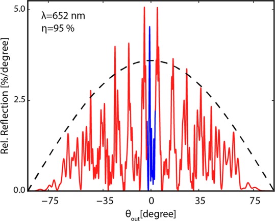
Broad-angle metasurface. Simulated angular scattering at λ = 652 nm in the far field for the broad-angle metasurface illuminated at normal incidence composed of diffracted (red) and specularly reflected (blue) light. The dashed black line shows the angular profile of a perfect Lambertian diffuser.
Experiment
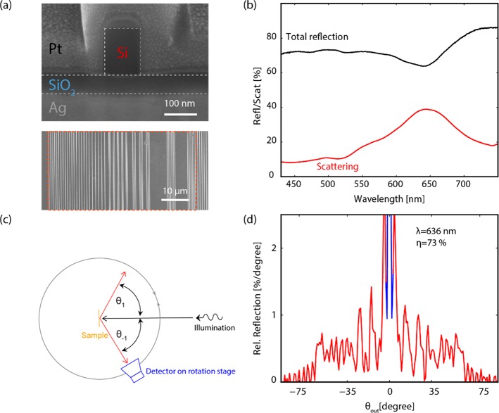
Thin layers of silver (200 nm), SiOx (110 nm), and silicon (185 nm) were deposited successively on a Si substrate by electron-beam thin-film deposition (Polyteknik Flextura Evaporator). After deposition, a 40 nm layer of HSQ was spin-coated on top of the silicon (Suss Microtec Delta 80 spin-coater), patterned by electron beam lithography (Raith Voyager 50 kV electron beam lithography system) and developed in TMAH at 50 °C for 1 min. After development, the rod geometry was transferred from the HSQ mask into the silicon using reactive ion etching (RIE) in a HBr2 (48.5 sccm) and O2 (1.5 sccm) plasma (Oxford PlasmaPro100 Cobra). The SiOx layer serves as an effective etch stop. The surface was fabricated in a 1.5 × 1.5 mm2 field. Figure 4(a) shows a cross-section secondary electron microscopy (SEM) image of a single Si rod and a top-view SEM image of the supercell composed of 7 different metagratings. To circumvent diffraction effects, each supercell of the metasurface is composed of a different arrangement of the same 7 metagratings. The distance between the supercells is varied from 720–7500 nm. The exact parameters of the structure for the broad-angle metasurface is listed in Table 1.
Figure 4.
Fabricated broad-angle metasurface and optical measurements. (a) Top: Cross-section SEM image of a silicon bar on a SiOx layer on Ag. To create image contrast. the sample was covered with platinum before performing the FIB cross-section. Bottom: Top-view SEM image. The red dashed box represents a supercell composed of 7 differently pitched metagratings. (b) Total reflection (black) and scattering excluding specular reflection (red). (c) Schematic of angular scattering setup. The sample in the center of a rotating stage is illuminated with a vertical tilt of 10° by a collimated p-polarized light beam (spectral bandwidth 2.5–5 nm). The detector on the rotating stage with a vertical tilt of −10° collects the reflected power at a given horizontal angle θout. (d) Measured angular reflection on resonance (λ = 636 nm). The red data indicate the diffracted scattering, and the blue data are specular reflection.
Optical reflection spectra were measured using an integrating sphere setup with the sample tilted 8° relative to the incoming collimated beam from a broad-band light source, to capture all scattered and specularly reflected light from the surface in the integrating sphere. Additional scattering measurements were made capturing only scattering into the grating orders (i.e., without specular reflection). In this case, the sample was placed without tilt at the back side of the integrating sphere, so that specularly reflected light was reflected out through the entrance opening of the integrating sphere. Figure 4(b) shows the measured total reflection and scattering spectra of the broad-angle reflecting surface. A clear scattering peak is observed around 636 nm, demonstrating the Mie-resonant nature of the metagrating geometry. The total reflectivity of the surface in the measured spectral range is 60–80%, with the remainder of impinging light being absorbed in the Ag back reflector and in the Si bars. This expectation is confirmed by the resonant dip in the total reflectivity at resonance.
The measurement setup for the angle-resolved reflection measurement is shown in Figure 4(c). A collimated, s-polarized beam of 636 nm light is incident on the sample surface. A detector (collection solid angle 0.0015 sr) positioned on a rotating stage around the sample allows angle-resolved measurements. In order to measure the specular reflection into the zeroth order, the beam is incident under a vertical angle tilt of 10° above the sample, and the detector is 10° below the sample. The angle-resolved measurement at the resonance wavelength [636 nm, bandwidth 2.5–5 nm, Figure 4(d)] shows an overall spectral shape similar to simulations. In the experiment, 73% of the total reflected power is scattered into the 5–65° angular range. We attribute the remaining specular reflectivity (27%) to the fact that a fixed SiOx thickness was used for all grating periods (while the optimum thickness decreases with pitch) and small fabrication inhomogeneities. The overall Lambertian shape can be approximated in experiments, but the specular reflection as well as small angle diffraction at 5° does not follow exactly the calculated trend. These limitations can be attenuated by using an advanced metagrating fabrication procedure to fully cancel the specular component. As mentioned earlier, the metagrating approach leads to a resonant behavior of the structure. Off-resonance, the metasurface shows very limited broad-angle scattering as is described below.
Large-Angle Reflector Metasurface
Numerical Simulation and Experimental Results
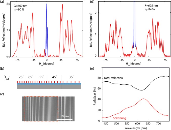
To illustrate the versatility of the metagrating design introduced here, which enables tailoring the angular scattering profile with large flexibility, we designed, fabricated, and measured a scattering metasurface that only scatters into a predefined range of large angles. Such functionality is highly beneficial, for example, in light trapping applications in solar cells, where incident sunlight must be coupled to the in-plane waveguide modes of the solar cell.31,32 The large-angle scattering metasurface is composed of 5 metagratings that steer light into the 35–75° angular range, with each metagrating composed of 5 unit cells including a single silicon rod. Figure 5(a) shows the numerical simulation of the far-field angular scattering distribution of a single supercell [see Figure 5(b)] near the Mie-resonant wavelength at 660 nm. In this design, more than 90% of the incident power is scattered toward the ±1 diffraction orders. An SEM top view of the fabricated large-angle metasurface is shown in Figure 5(c). The measured angular reflection [Figure 5(d)] shows the same trend as in simulations; 84% of the light is scattered into large-angle diffraction orders at resonance. The total reflection and scattering measurement data are shown in Figure 5(e) and clearly prove the resonant scattering nature of the large-angle metasurface.
Figure 5.
Large-angle reflector metasurface. (a) Numerical simulations of the angular reflection in far field for a single supercell of the large-angle reflector. (b) Schematic of the supercell. (c) SEM top view of the fabricated metasurface; the orange dashed box indicates a single supercell. (d) Angular reflection on resonance (λ = 625 nm). The red data indicate the diffracted scattering, and the blue data are specular reflection. (e) Total reflection (black) and scattering without specular reflection (red) of the large-angle reflector.
Off-Resonance Optical Performance of Metasurfaces
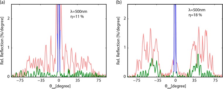
As mentioned earlier, the metagrating design is based on resonant scattering from the building blocks. Figure 6 shows off-resonance (λ = 500 nm) reflection measurements of the broad-angle reflector and the large-angle reflector, overlaid with the resonant data presented above, i.e., Figures 4d and 5d, respectively. The integrated off-resonance scattering efficiencies toward the grating orders are only 11% and 18% for two respective designs. This clearly shows that the proposed metagrating works on the principle of resonant scatterers. The existing off-resonance nonspecular scattering of the structure can be explained by the broad line width of the magnetic dipole resonance of the silicon rods, as well as the existence of higher order modes that were not considered in the design.
Figure 6.
Measured angular reflection of the broad-angle reflector (a) and the large-angle reflector (b), off-resonance at λ = 500 nm. Diffracted scattering (green) and specular reflection (blue) contributions are shown. Data for resonant excitation [λ = 650 nm, same as Figures 4(d) and 5(d)] are overlaid for reference (red).
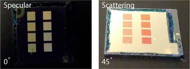
A demonstration of the metagrating working as a “nanostructured paint” can be seen in the abstract graphic, which shows two photographs of the same sample, with 4 fields of broad-angle scattering metasurfaces in the left row and 4 fields of large angle scattering metasurfaces in the right row, respectively. The dimensions between the fields vary slightly due to a different choice of electron dose in the electron beam lithography writing. The SEM images and optical measurements of the two lowest fields are shown in this Article. In both photos, unpolarized white light is incident from the top, perpendicular to the sample. In the first photo, the specular reflection is captured by taking a photo from the top; in the second photo, the scattering created by the metagratings is captured under an angle (around 45°). The color change visible in the photos indicates that only the color around the resonance (orange) is scattered sideways, and the rest of the spectrum (blueish, due to removed orange part of the spectrum) is reflected specularly.
Discussion and Conclusions
In this work, we demonstrated metasurfaces composed of combined metagratings with tailored angular scattering profiles. Based on a theoretical dipole scattering model, we designed these ultrathin surfaces to realize broad-angle and large-angle scattering profiles. Using nanofabrication, we created Si Mie resonators on a Ag backplane and arranged the differently pitched metagratings in a supercell geometry to scatter light over the desired broad angular range. Combining multiple scatterers within a metagrating unit cell allows further control of the angular response, suppressing higher-order diffraction modes. Specular reflection is strongly suppressed, with 73% and 84% of the incident light scattered into the defined set of angles on resonance, for the broad-angle and large-angle geometries, respectively. Based on the same principles introduced here, extension of the design to 3D functionality and dual polarization can be readily explored. For example, 3D cylinders as scattering units have polarization independent resonance behavior, and they could be placed in hexagonal grids to enable functionality on 3 axes. A further natural step for this work is to realize transparent resonant metagratings by controlling the interaction between suitable stacked Mie resonators, to replace the reflective back plane, in applications where transparency in the off-resonant spectral band is required.
Due to their high scattering efficiency and resonant operation, metagratings can be used in a wide range of applications. The ultrathin resonant metastructures effectively create the functionality of “nanostructured paint”, which can find applications in photovoltaics with colored appearance, a topic of great interest recently. By combining metasurfaces with different resonance wavelengths, multiple colored pixels may be envisioned, as well as diffuse surfaces with a white appearance.26 Similarly, due to the spectral sensitivity, the presented metasurfaces can serve as spectrum splitting architectures in tandem solar cells. Furthermore, the large-angle scattering design can serve to enhance light trapping in thin-film solar cells, improving the effectiveness of coupling to in-plane waveguide modes. Many other applications in geometries that require a tailored (colored) scattering appearance come to mind as well, for example, in controlling emission profiles in solid-state lighting and signaling where the spectral and directional control of light is important.
The metagrating geometry introduced here, with many different length scales, can be readily fabricated in larger volumes using substrate conformal soft imprint lithography (SCIL).33 A full metagrating master pattern is then first made in a silicon wafer using electron beam lithography, from which a soft imprint stamp is then made that can transfer the pattern into a silica sol–gel that serves as a mask for metasurface etching. Similarly, light scattering metagratings may be directly patterned using SCIL in a suitable high-index sol–gel layer.
Acknowledgments
This work is part of the research program of the “Nederlandse organisatie voor Wetenschappelijk Onderzoek” (NWO). It is also funded by the Global Climate and Energy Project (GCEP) and the European Research Council (ERC). Y.R. and A.A. were supported in part by the Air Force Office of Scientific Research, the National Science Foundation, and the Welch Foundation with grant No. F-1802.
Supporting Information Available
The Supporting Information is available free of charge on the ACS Publications website at DOI: 10.1021/acsphotonics.8b01795.
Details about derivation of design equation, analytical antenna theory, and optimization of structure by simulation (PDF)
The authors declare no competing financial interest.
Supplementary Material
References
- Berger O.; Inns D.; Aberle A. G. Commercial white paint as back surface reflector for thin-film solar cells. Sol. Energy Mater. Sol. Cells 2007, 91 (13), 1215–1221. 10.1016/j.solmat.2007.04.008. [DOI] [Google Scholar]
- Wang M.; Ye X.; Wan X.; Liu Y.; Xie X. Brilliant white polystyrene microsphere film as a diffuse back reflector for solar cells. Mater. Lett. 2015, 148, 122–125. 10.1016/j.matlet.2015.02.063. [DOI] [Google Scholar]
- Cao H.; et al. Ultraviolet lasing in resonators formed by scattering in semiconductor polycrystalline films. Appl. Phys. Lett. 1998, 73 (25), 3656–3658. 10.1063/1.122853. [DOI] [Google Scholar]
- Garcia P. D.; Sapienza R.; Lopez C. Photonic Glasses: A Step Beyond White Paint. Adv. Mater. 2010, 22 (1), 12–19. 10.1002/adma.200900827. [DOI] [PubMed] [Google Scholar]
- Wiersma D. S.; Bartolini P.; Lagendijk A.; Righini R. Localization of light in a disordered medium. Nature 1997, 390 (6661), 671–673. 10.1038/37757. [DOI] [Google Scholar]
- Schwartz T.; Bartal G.; Fishman S.; Segev M. Transport and Anderson localization in disordered two-dimensional photonic lattices. Nature 2007, 446 (7131), 52–55. 10.1038/nature05623. [DOI] [PubMed] [Google Scholar]
- Miranda-Muñoz J. M.; Lozano G.; Míguez H. Design and Realization of a Novel Optically Disordered Material: A Demonstration of a Mie Glass. Adv. Opt. Mater. 2017, 5 (10), 1700025. 10.1002/adom.201700025. [DOI] [Google Scholar]
- Moccia M.; et al. Coding Metasurfaces for Diffuse Scattering: Scaling Laws, Bounds, and Suboptimal Design. Adv. Opt. Mater. 2017, 5 (19), 1700455. 10.1002/adom.201700455. [DOI] [Google Scholar]
- Moccia M.; et al. Suboptimal Coding Metasurfaces for Terahertz Diffuse Scattering. Sci. Rep. 2018, 8 (1), 11908. 10.1038/s41598-018-30375-z. [DOI] [PMC free article] [PubMed] [Google Scholar]
- Chen K.; et al. Geometric phase coded metasurface: from polarization dependent directive electromagnetic wave scattering to diffusion-like scattering. Sci. Rep. 2016, 6 (1), 35968. 10.1038/srep35968. [DOI] [PMC free article] [PubMed] [Google Scholar]
- Pors A.; Ding F.; Chen Y.; Radko I. P.; Bozhevolnyi S. I. Random-phase metasurfaces at optical wavelengths. Sci. Rep. 2016, 6 (1), 28448. 10.1038/srep28448. [DOI] [PMC free article] [PubMed] [Google Scholar]
- Kwon H.; Arbabi E.; Kamali S. M.; Faraji-Dana M.; Faraon A. Computational complex optical field imaging using a designed metasurface diffuser. Optica 2018, 5 (8), 924. 10.1364/OPTICA.5.000924. [DOI] [Google Scholar]
- Jang M.; et al. Wavefront shaping with disorder-engineered metasurfaces. Nat. Photonics 2018, 12 (2), 84–90. 10.1038/s41566-017-0078-z. [DOI] [PMC free article] [PubMed] [Google Scholar]
- Mohammadi Estakhri N.; Alù A. Wave-front Transformation with Gradient Metasurfaces. Phys. Rev. X 2016, 6 (4), 041008. 10.1103/PhysRevX.6.041008. [DOI] [Google Scholar]
- Asadchy V. S.; Albooyeh M.; Tcvetkova S. N.; Díaz-Rubio A.; Ra’di Y.; Tretyakov S. A. Perfect control of reflection and refraction using spatially dispersive metasurfaces. Phys. Rev. B: Condens. Matter Mater. Phys. 2016, 94 (7), 075142. 10.1103/PhysRevB.94.075142. [DOI] [Google Scholar]
- Epstein A.; Eleftheriades G. V. Huygens’ metasurfaces via the equivalence principle: design and applications. J. Opt. Soc. Am. B 2016, 33 (2), A31. 10.1364/JOSAB.33.000A31. [DOI] [Google Scholar]
- Ra’di Y.; Sounas D. L.; Alù A. Metagratings: Beyond the Limits of Graded Metasurfaces for Wave Front Control. Phys. Rev. Lett. 2017, 119 (6), 067404. 10.1103/PhysRevLett.119.067404. [DOI] [PubMed] [Google Scholar]
- Epstein A.; Rabinovich O. Unveiling the Properties of Metagratings via a Detailed Analytical Model for Synthesis and Analysis. Phys. Rev. Appl. 2017, 8 (5), 054037. 10.1103/PhysRevApplied.8.054037. [DOI] [Google Scholar]
- Sell D.; Yang J.; Doshay S.; Yang R.; Fan J. A. Large-Angle, Multifunctional Metagratings Based on Freeform Multimode Geometries. Nano Lett. 2017, 17 (6), 3752–3757. 10.1021/acs.nanolett.7b01082. [DOI] [PubMed] [Google Scholar]
- Yang J.; Sell D.; Fan J. A. Freeform Metagratings Based on Complex Light Scattering Dynamics for Extreme, High Efficiency Beam Steering. Ann. Phys. 2018, 530 (1), 1700302. 10.1002/andp.201700302. [DOI] [Google Scholar]
- Rabinovich O.; Epstein A. Analytical Design of Printed Circuit Board (PCB) Metagratings for Perfect Anomalous Reflection. IEEE Trans. Antennas Propag. 2018, 66 (8), 4086–4095. 10.1109/TAP.2018.2836379. [DOI] [Google Scholar]
- Khaidarov E.; et al. Asymmetric Nanoantennas for Ultrahigh Angle Broadband Visible Light Bending. Nano Lett. 2017, 17 (10), 6267–6272. 10.1021/acs.nanolett.7b02952. [DOI] [PubMed] [Google Scholar]
- Liu W.; Miroshnichenko A. E. Beam Steering with Dielectric Metalattices. ACS Photonics 2018, 5 (5), 1733–1741. 10.1021/acsphotonics.7b01217. [DOI] [Google Scholar]
- Paniagua-Domínguez R.; et al. A Metalens with a Near-Unity Numerical Aperture. Nano Lett. 2018, 18 (3), 2124–2132. 10.1021/acs.nanolett.8b00368. [DOI] [PubMed] [Google Scholar]
- Neder V.; Luxembourg S. L.; Polman A. Efficient colored silicon solar modules using integrated resonant dielectric nanoscatterers. Appl. Phys. Lett. 2017, 111 (7), 073902. 10.1063/1.4986796. [DOI] [Google Scholar]
- Neder V.; Luxembourg S. L.; Polman A.. Colored solar modules using integrated pixelated resonant dielectric nanoscatterer arrays. In 33rd European Photovoltaic Solar Energy Conference and Exhibition, 2017; pp 34–37. [Google Scholar]
- Cao L.; Fan P.; Barnard E. S.; Brown A. M.; Brongersma M. L. Tuning the Color of Silicon Nanostructures. Nano Lett. 2010, 10 (7), 2649–2654. 10.1021/nl1013794. [DOI] [PubMed] [Google Scholar]
- Proust J.; Bedu F.; Gallas B.; Ozerov I.; Bonod N. All-Dielectric Colored Metasurfaces with Silicon Mie Resonators. ACS Nano 2016, 10 (8), 7761–7767. 10.1021/acsnano.6b03207. [DOI] [PubMed] [Google Scholar]
- Sun S.; et al. All-Dielectric Full-Color Printing with TiO 2 Metasurfaces. ACS Nano 2017, 11 (5), 4445–4452. 10.1021/acsnano.7b00415. [DOI] [PubMed] [Google Scholar]
- Kuznetsov A. I.; Miroshnichenko A. E.; Fu Y. H.; Zhang J.; Luk’yanchuk B. Magnetic light. Sci. Rep. 2012, 2, 1–6. 10.1038/srep00492. [DOI] [PMC free article] [PubMed] [Google Scholar]
- Callahan D. M.; Munday J. N.; Atwater H. A. Solar cell light trapping beyond the ray optic limit. Nano Lett. 2012, 12 (1), 214–218. 10.1021/nl203351k. [DOI] [PubMed] [Google Scholar]
- Brongersma M. L.; Cui Y.; Fan S. Light management for photovoltaics using high-index nanostructures. Nat. Mater. 2014, 13 (5), 451–460. 10.1038/nmat3921. [DOI] [PubMed] [Google Scholar]
- Verschuuren M. A.; Megens M.; Ni J. F.; van Sprang H.; Polman A. Large area nanoimprint by substrate conformal imprint lithography (SCIL). Adv. Opt. Technol. 2017, 3. 10.1515/aot-2017-0022. [DOI] [Google Scholar]
Associated Data
This section collects any data citations, data availability statements, or supplementary materials included in this article.


