Photon pairs are generated in an electrically driven tunnel junction.
Abstract
Generating time-correlated photon pairs at the nanoscale is a prerequisite to creating highly integrated optoelectronic circuits that perform quantum computing tasks based on heralded single photons. Here, we demonstrate fulfilling this requirement with a generic tip-surface metal junction. When the junction is luminescing under DC bias, inelastic tunneling events of single electrons produce a stream of visible photons of plasmonic origin whose superbunching index is 17 (improved to a record of 70 by the authors during publication) when measured with a 53-ps instrumental resolution limit. The effect is driven electrically, rather than optically. This discovery has immediate and profound implications for quantum optics and cryptography, notwithstanding its fundamental importance to basic science and its ushering in of heralded photon experiments on the nanometer scale.
INTRODUCTION
Tunnel junctions are important light sources in their own right that convert electric potential energy into photons, largely through one electron–one photon (1e− → 1γ) inelastic tunneling events. These junctions facilitate many intricate fundamental processes such as time-correlated two-electron tunneling (1, 2), overbias emission (3–5), photon antibunching in single-photon emitting molecular systems (6, 7), and photon bunching from dynamical processes that modulate junction properties, such as molecular motion (8, 9). These emission processes arise from how stochastic fluctuations couple to the electromagnetic modes of an environment (10), which imprint characteristic deviations away from Poissonian statistics onto the temporal correlations in the emitted photon stream. Critically missing from these examples is a 1e− → nγ process, where a single electron manifestly produces multiple photons. The simplest of these is the 1e− → 2γ process. Using scanning tunneling microscopy (STM)–induced luminescence techniques (11) to examine the light from atomically flat metal junctions, we detect a non-Poissonian process that manifests as photon superbunching, which, in tandem, evidences emission of time-correlated photon pairs from a tunnel junction formed between metals. The effect is reminiscent of two-mode squeezed photon pairs (12), but without externally applied AC voltages and the energy constraints imposed by millikelvin temperatures. Its detection now expands the inventory of fundamental processes that can be controlled in a tunnel junction environment.
RESULTS
The superbunching and its characterization are obtained with the experimental setup (13) shown in Fig. 1. The surface topography and spectroscopic characterization of a clean Ag(111) single crystal obtained with STM are shown in Fig. 2 (A and B, respectively). The light radiating from the junction (orange curve) due to the tunnel current is recorded while sweeping the bias from 1 to 10 V, holding the current constant with a feedback loop. The feedback causes the tip to retract from the surface in a step-like fashion (purple curve) due to field emission resonance (FER) states (green curve) at metal surfaces with a bandgap near the vacuum level (14). The succession of these FER states introduces oscillatory variations in the electronic density of states. Note that the total light emission intensity (orange curve) drops substantially from its maximum near 3 V when the voltage approaches the first FER state. Our measurement reproduces the essential, known features of a metal-metal tunnel junction (15, 16).
Fig. 1. Schematic of a scanning tunneling microscope combined with a Hanbury Brown and Twiss interferometer.
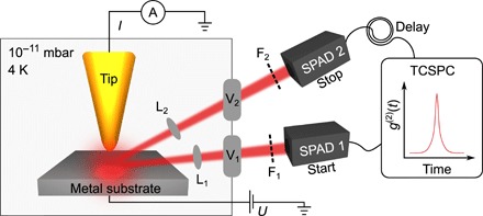
Light radiating from a junction formed between a gold tip and Ag(111) substrate travels along two optical paths (1, 2) through a series of lenses (L), viewports (V), and optical filters (F) to a pair of single-photon avalanche diodes (SPADs). The number of photon coincidence events as a function of time delay t between the SPADs, g(2)(t), is measured with a time-correlated single-photon counter (TCSPC). The voltage bias (U) is applied to the substrate. The tunnel current (I) is measured with a picoammeter (A). A third optical path to an optical spectrometer is not shown.
Fig. 2. Tunnel junction characterization with photon pair generation schematic.
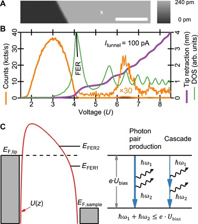
(A) Ag(111) surface topography with a monatomic step imaged at 3 V, 100 pA. X marks the position of bunching measurements. Scale bar, 5 nm. The gradation spans one 240-pm Ag terrace step height. (B) Total light intensity (orange), tip retraction (purple), and density of states (DOS; green) during a linear voltage sweep at constant current. The position of the first FER maximum is indicated with a black line. arb. units, arbitrary units. kcts, kilocounts. (C) An energy level diagram of an inelastic electron tunneling event leading to photon pair production. The junction is biased by a fixed Ubias voltage. An electron at the tip Fermi level (EF,tip) tunnels through a junction potential barrier U(z), where z is a position in the gap, arriving on the sample side with an energy E = e · Ubias above the sample Fermi level (EF,sample). E can be aligned or misaligned with FERs nearby. E is an upper bound for the total photon energy because metals provide a continuum of initial and final states.
The temporal photon intensity correlation function g(2)(t) that evidences photon superbunching is measured with a Hanbury Brown and Twiss interferometer (17) (Fig. 1) by collating the distribution of times t between one photon arriving at the start detector [single-photon avalanche diode 1 (SPAD 1)] and another photon arriving at the stop detector (SPAD 2) (6). Two photon counters are necessary to confirm simultaneously generated photons since the instrumental dead time is ~76 ns (see Materials and Methods). A temporal correlation event registers when both detectors sense one photon each, typically with a nanosecond time delay between the sensing. While accidental coincidences may occur at any relative time delay (as they involve uncorrelated photons), true coincidences require two emitted photons arriving simultaneously and manifest as a sharp feature in g(2)(t) at time zero. These special pairs can be produced according to the schematic shown in Fig. 2C. An inelastic tunneling process can excite tip-localized plasmon modes that subsequently decay into photons detected in the far field. In addition to well-known single-photon emission, bunched emission can occur whenever photon pairs are produced, such as in an idealized two-step cascade that produces one photon in each step (18).
Figure 3A shows the measured g(2)(t) for our tunnel junction light source derived from time-correlated single-photon counting, and plotted with coincidence events as a function of time between photon detection at the start and stop SPADs. Because the counting statistics of electron transport in a tunnel junction is Poissonian (19), the absence of an antibunching feature at time t = 0 is expected. However, the presence of a bunching feature is not. It signals that electroluminescence in a generic tunnel junction does not occur solely in the form of individual 1e− → 1γ events. While observing g(2)(0) > 1 is already indicative of bunched photon emission, g(2)(0) = 17 (also in Fig. 3A) shows that the photons are unambiguously superbunched (20). The existence of photon bunches containing at least pairs of photons is evidenced by the two independent SPADs detecting light within less than 53 ps of each other. While a bunch may contain more than two photons and may obey certain quantum mechanical relationships, these possibilities remain uncharacterized by the current experiment. Nevertheless, the high bunching ratio g(2)(0) is distinct from that generated by chaotic light sources, for which g(2)(t) ≤ 2 holds. The set point of 4.63 V, 20 nA is representative of a broad range of tunnel parameters where superbunching is observable. The bunching feature has an even narrower width than the reference correlation measured with light pulses from a picosecond white light source, thus indicating that the bunching peak shape is even closer to the instrumental response function than the reference measurement (blue curve in Fig. 3B; Materials and Methods). Thus, the peak value of g(2)(0) is limited by the detectors’ time resolution and may be substantially larger if detection with higher time resolution is used. Using g(2)(0) as a coincidence-to-accidental events ratio, this metric is already comparable to photon pair sources based on cooled optical fibers, which can perform quantum key distribution with a 3% bit error rate (21).
Fig. 3. Photon correlation measurements of a tunnel junction and picosecond light source.
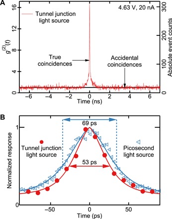
(A) Typical g(2)(t) measurement for the tunnel junction light source. The total number of true coincidence events (2620) is determined by integrating between ±1 ns after subtracting the level of accidental coincidence events (18.6) that corresponds to (black line) and is equal to the product of the two SPAD count rates. Total data accumulation time of 29,400 s. (B) A comparison of g(2)(t) rescaled to have unity peak height for the tunnel junction source (red) and an autocorrelation of a commercial picosecond white light source with 6-ps fundamental pulse width (blue). The full widths at half maxima are indicated. Solid lines are guides for the eye.
Next, we characterize how the true and accidental coincidence events vary as a function of tunnel current. The raw data and resulting series are shown in Fig. 4. For each new current, the bias is adjusted slightly to tunnel elastically into the first FER maximum (16). Note that for any STM measurement, only two of the current, voltage, and tip-sample distance tunnel parameters can serve as independent variables. This requires adjusting both the current and voltage simultaneously when following a particular spectroscopic feature that is not pinned by the substrate Fermi energy. Bunching is best observed when the total light intensity is made low (22), either by reducing the tunnel current (Figs. 3A, 4A, and 4F) or, in tandem, leveraging the broad, low but nonzero minimum between 4 and 6 V in the light intensity curve (Fig. 2B, orange). Although we chose to follow the position of the first FER state in our measurements, bunching does not seem to be predicated on populating any FER state because it is visible even at 3.2 V, which is far below the first FER maximum.
Fig. 4. Photon correlation measurements as a function of current.
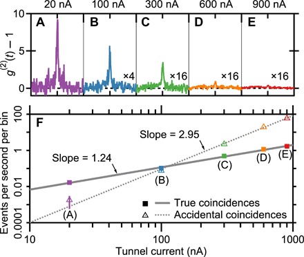
(A to E) The measured function g(2)(t) − 1 is for the currents shown. The unity shift aligns the normalized accidental coincidence level to zero across all measurements for ease of comparison. The horizontal axis in each window spans ±1-ns time delay t. Respective voltages of 4.47, 4.60, 4.65, 4.70, and 4.74 V are applied in (A) to (E). (F) Log-log plot of the absolute number of true and accidental coincidence events versus current. Both have a power-law dependence on the current equal to the slope of the fitted lines. The ratio of each data point pair yields the respective g(2)(0) − 1 peak values of 9.2, 1.4, 0.22, 0.060, and 0.028 for each trace from (A) to (E). Total data accumulation time of 1200 s (A to C) and 600 s (D and E).
DISCUSSION
Figure 4 (A to E) shows the measured quantity g(2)(t) − 1. From right to left, the bunching peak value increases with decreasing current. Focusing on Fig. 4F, the power-law exponent for true coincidences (1.24) is less than half of the value for accidental coincidences (2.95), implying that bunching is due to single-electron tunneling events, and, for this reason, it will dominate at low current. Let I be the current, e the electric charge, k1 the quantum efficiency for emitting a single photon, and η the effective probability that this photon is detected. Without loss of generality, η for both detectors is assumed to be equal. The number of single-photon events per second is N1 = Ik1η/e; hence, the number of accidental coincidences per second is = τ = (Ik1η/e)2τ, where τ is the binning time interval of the correlation measurement. In contrast, the number of true coincidence events per second is N2 = Ik2η2/e, where k2 is the quantum efficiency for emitting a photon pair. N2 is also equal to the area of g(2)(t) − 1. We further assume that k2 ≪ k1 ≪ 1. The ratio of time-correlated pairs to accidental coincidences is then and does not involve the detector efficiency η.
First, if the photon pair is assumed to originate from a cascade of two independent emission events with the same quantum efficiency, then k2 = . This scenario corresponds to photon pair emission decomposable into two single-photon events, which we regard herein as a “trivial” process. But actually, our measurements show that k2 = 215 (Fig. 3A) can be two orders of magnitude larger than . Moreover, if the tunneling electron loses energy in an emission process, then it tends to fall deeper into a classically forbidden state with exponentially smaller amplitude than the initial state. This reduces the probability for a second photon emission. Calculations suggest a reduction by about three orders of magnitude (see Supplementary Text and fig. S1). This scenario makes the observed k2 about five orders of magnitude larger than one would expect.
Second, examining the formulas for accidental and true coincidences, we can directly compare the current dependencies of and k2, which correspond to emitting two single photons versus one photon pair. Figure 4F shows that (Ik1η/e)2 ~ I2.95 and (Ik2η2/e) ~ I1.24, so that empirically, k1 ~ I0.475 and k2 ~ I0.24 rather than , as one would expect for a cascade process. These two observations decisively argue against the cascade emission mechanism, that is, the photon pair is not composed of 1e− → 1γ processes. Hence, excluding this possibility evidences a 1e− → 2γ process being operant—a coherent simultaneous pair emission process—and raises fundamental questions about how nontrivial two-photon processes may arise.
As a consistency check, g(2)(t) is measured with and without intervening optical shortpass filters (F1 and F2 in Fig. 1) with cutoffs exceeding half the applied tunnel voltage. This tests whether positive correlations occur for photon pairs whose total energy exceeds the energy of one tunneling electron. Figure 5 shows the light spectrum obtained with e · Ubias = 4 eV tunneling electrons that exhibits bunching (orange; parts A and B), while the filtered spectrum with a 2.07-eV cutoff does not (green; parts A and C). Hence, in a bunch (or pair) of photons, not more than one photon carries more than half of the electron energy. Bunching is seen if the experiment is repeated but with one shortpass replaced with a longpass filter (fig. S2). This complementary result shows that while bunches do not contain two higher-energy photons, one higher-energy photon can pair up with a lower-energy photon, and thus, higher-energy photons unambiguously participate in the bunching. If this pairing arises from spontaneous two-photon emission analogous to those of atomic systems, then the pairs are entangled due to energy and angular momentum conservation (23). In lieu of a complete assessment of the two photons across all quantum variables (24, 25), the true nature of the photon pairs is a new, open question that has arisen from a system that has been studied for over 40 years (26).
Fig. 5. Photon correlation measurements at fixed tunnel conditions with varied spectral filtering.
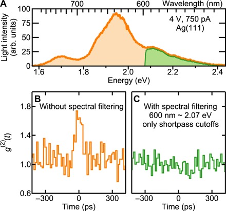
(A) Measured optical spectrum (orange) and its shortpass 600-nm cutoff spectrum (green). (B) Bunching is observed in the unfiltered light. (C) Bunching is not observed when the low-energy photons are blocked for both detectors (F1 = F2 = shortpass filter in Fig. 1), and the total energy of a photon pair is required to exceed the electron energy of 4 eV. Total data accumulation time in seconds: (B) 600 and (C) 39,000. Accidental correlation level in events per bin: (B) 42.05 and (C) 107.7.
The measurement with spectral filtering (Fig. 5) reaffirms that the bunched photons do not originate from time-correlated 1e− → 1γ processes and, again, evidences the 1e− → 2γ process being operant. Even bunching from coordinated electron tunneling is unlikely because this process is quadratic in the current (27). We speculate that photon pair creation may be possible due to spontaneous parametric down-conversion of plasmon polaritons (28), which is enabled by the optical nonlinearity of the nanometer tunnel junction between the metals (29), with the small tip extension alleviating phase-matching conditions. The presence of optical resonances in the junction at energies corresponding to about half the high tunneling electron energies available (Fig. 5A) will further increase the matrix elements for pair emission.
Confirming the existence of a 1e− → 2γ electroluminescent process in the Au-Ag(111) junction is the key to rationalizing our bunching observations. Such a process evidences photon pairs being emitted much closer to each other than the ~50-ps temporal resolution of our experiments. This result validates that simple tunnel junctions do behave as special light emitters beyond their established domain. We have also observed bunching from junctions formed by other metallic elements (figs. S2 and S3). Using quantum efficiency and energy conservation arguments, we demonstrated that photon pairs can originate from an intrinsic elementary process with fast temporal characteristics without invoking bulk optical media with strong second- or third-order nonlinearities (30).
Our results show that an optoelectronic component useful for quantum computing (31, 32) can be miniaturized substantially and controlled at the atomic scale (Fig. 2A). Photon entanglement (33, 34) and heralding measurements (35, 36) that require double- or higher-photon coincidences may now be possible at the nanoscale; the coincidence rate in Fig. 3A is already sufficient to accomplish the former (37). Using broader tip apexes (38), the photon energy may shift to where optical fibers have minimal transmission loss (C band, 1530 to 1565 nm) and synergize with contemporary developments in optical communications (39). We anticipate that these findings herein will further motivate using tunnel junctions as novel photonic devices in nanoscience.
MATERIALS AND METHODS
Peripherals
The STM-induced luminescence setup was equipped with a pair of spectrally integrating, SPADs (Micro Photon Devices PD 100 CTE; supplier-measured 29- and 33-ps full width at half maximum time resolution, 74.9- and 76.8-ns dead time) and an optical spectrograph (Acton Research Spectra Pro 900i; 150 lines/mm blazed grating with Peltier-cooled, intensified charge-coupled device). In all optical spectra shown, no correction was made for variations in the wavelength dependence of the detection efficiency. Photon correlation measurements were obtained with hardware (SPC-130, Becker & Hickl) configured in start-stop mode with a 12.2-ps time bin width throughout this study. A white light source (Fianium WhiteLase, WL-SC-400-40; 80-MHz repetition rate, 6-ps fundamental pulse width) filtered by a variable bandpass monochromator (Fianium LLTF Contrast VIS; <2.5-nm spectral bandwidth) generated the 690-nm pulses used in the reference measurement shown in Fig. 3B (in blue).
Tunnel junction
A Ag(111) single crystal, oriented to 0.1°, was cleaned via repeated cycles of Ar+ sputtering between 300 and 400 K, followed by annealing to 900 K in an ultrahigh vacuum preparation chamber. It was then transferred in situ to the scanning tunneling microscope and checked for surface cleanliness (Fig. 2A). Tips were prepared by electrochemically etching ⌀0.25 mm, 99.995% pure Au wire, followed by repeated indenting and voltage pulsing on Ag(111). Differential conductance (dI/dU) measurements, in which the signal is proportional to the density of electronic states, were made by modulating the bias voltage (211 Hz, 20 mV peak to peak) and recording the lock-in signal in the current. All voltages were applied to the Ag substrate with the tip held at 0 V. All measurements were reproducibly tunable via STM parameters such as voltage and current excluding tip modification. We performed experiments with the tip positioned above a flat terrace rather than at defects with the benefit of making the measurements robust against the tip position drifting.
Supplementary Material
Acknowledgments
Funding: The authors have no funding sources to declare. Author contributions: C.C.L., A.R., and A.G. performed the experimental work. O.G. performed the comparison with the cascade emission model. C.C.L. analyzed the data and wrote the manuscript with input from all authors. K.Ku. and K.Ke. conceived and designed the research program. Competing interests: The authors declare that they have no competing interests. Data and materials availability: All data needed to evaluate the conclusions in the paper are present in the paper and/or the Supplementary Materials. Additional data related to this paper may be requested from the authors.
SUPPLEMENTARY MATERIALS
Supplementary material for this article is available at http://advances.sciencemag.org/cgi/content/full/5/5/eaav4986/DC1
Supplementary Text
Fig. S1. Schematic of a one-dimensional model of tunneling.
Fig. S2. Photon correlation measurements at fixed tunnel conditions with varied spectral filtering for a gold tip on Au(111).
Fig. S3. Survey measurements of bunching for a gold tip on Cu(111).
REFERENCES AND NOTES
- 1.Kaasbjerg K., Nitzan A., Theory of light emission from quantum noise in plasmonic contacts: Above-threshold emission from higher-order electron-plasmon scattering. Phys. Rev. Lett. 114, 126803 (2015). [DOI] [PubMed] [Google Scholar]
- 2.Xu F., Holmqvist C., Rastelli G., Belzig W., Dynamical Coulomb blockade theory of plasmon-mediated light emission from a tunnel junction. Phys. Rev. B 94, 245111 (2016). [Google Scholar]
- 3.Dong Z. C., Zhang X. L., Gao H. Y., Luo Y., Zhang C., Chen L. G., Zhang R., Tao X., Zhang Y., Yang J. L., Hou J. G., Generation of molecular hot electroluminescence by resonant nanocavity plasmons. Nat. Photonics 4, 50–54 (2010). [Google Scholar]
- 4.Peters P.-J., Xu F., Kaasbjerg K., Rastelli G., Belzig W., Berndt R., Quantum coherent multielectron processes in an atomic scale contact. Phys. Rev. Lett. 119, 066803 (2017). [DOI] [PubMed] [Google Scholar]
- 5.Schull G., Néel N., Johansson P., Berndt R., Electron-plasmon and electron-electron interactions at a single atom contact. Phys. Rev. Lett. 102, 057401 (2009). [DOI] [PubMed] [Google Scholar]
- 6.Merino P., Große C., Rosławska A., Kuhnke K., Kern K., Exciton dynamics of C60-based single-photon emitters explored by Hanbury Brown-Twiss scanning tunnelling microscopy. Nat. Commun. 6, 8461 (2015). [DOI] [PMC free article] [PubMed] [Google Scholar]
- 7.Zhang L., Yu Y.-J., Chen L.-G., Luo Y., Yang B., Kong F.-F., Chen G., Zhang Y., Zhang Q., Luo Y., Yang J.-L., Dong Z.-C., Hou J. G., Electrically driven single-photon emission from an isolated single molecule. Nat. Commun. 8, 580 (2017). [DOI] [PMC free article] [PubMed] [Google Scholar]
- 8.Silly F., Charra F., Time-autocorrelation in scanning-tunneling-microscope-induced photon emission from metallic surface. Appl. Phys. Lett. 77, 3648 (2000). [Google Scholar]
- 9.Perronet K., Schull G., Raimond P., Charra F., Single-molecule fluctuations in a tunnel junction: A study by scanning-tunnelling-microscopy–induced luminescence. Europhys. Lett. 74, 313–319 (2006). [Google Scholar]
- 10.Jin J., Marthaler M., Schön G., Electroluminescence and multiphoton effects in a resonator driven by a tunnel junction. Phys. Rev. B 91, 085421 (2015). [Google Scholar]
- 11.Kuhnke K., Große C., Merino P., Kern K., Atomic-scale imaging and spectroscopy of electroluminescence at molecular interfaces. Chem. Rev. 117, 5174–5222 (2017). [DOI] [PubMed] [Google Scholar]
- 12.Forgues J.-C., Lupien C., Reulet B., Emission of microwave photon pairs by a tunnel junction. Phys. Rev. Lett. 113, 043602 (2014). [DOI] [PubMed] [Google Scholar]
- 13.Kuhnke K., Kabakchiev A., Stiepany W., Zinser F., Vogelgesang R., Kern K., Versatile optical access to the tunnel gap in a low temperature scanning tunneling microscope. Rev. Sci. Instrum. 81, 113102 (2010). [DOI] [PubMed] [Google Scholar]
- 14.Chulkov E. V., Borisov A. G., Gauyacq J. P., Sánchez-Portal D., Silkin V. M., Zhukov V. P., Echenique P. M., Electronic excitations in metals and at metal surfaces. Chem. Rev. 106, 4160–4206 (2006). [DOI] [PubMed] [Google Scholar]
- 15.Berndt R., Gimzewski J. K., Isochromat spectroscopy of photons emitted from metal surfaces in an STM. Ann. Phys. 2, 133–140 (1993). [Google Scholar]
- 16.Martínez-Blanco J., Fölsch S., Light emission from Ag(111) driven by inelastic tunneling in the field emission regime. J. Phys. Condens. Matter 27, 255008 (2015). [DOI] [PubMed] [Google Scholar]
- 17.Hanbury Brown R., Twiss R. Q., Interferometry of the intensity fluctuations in light II. An experimental test of the theory for partially coherent light. Proc. R. Soc. London, Ser. A 243, 291–319 (1958). [Google Scholar]
- 18.Zhang X., Xu C., Ren Z., A simple and general strategy for generating frequency-anticorrelated photon pairs. Sci. Rep. 6, 24509 (2016). [DOI] [PMC free article] [PubMed] [Google Scholar]
- 19.Bomze Yu., Gershon G., Shovkun D., Levitov L. S., Reznikov M., Measurement of counting statistics of electron transport in a tunnel junction. Phys. Rev. Lett. 95, 176601 (2005). [DOI] [PubMed] [Google Scholar]
- 20.McNeil K. J., Walls D. F., Possibility of observing enhanced photon bunching from two photon emission. Phys. Lett. A 51, 233–234 (1975). [Google Scholar]
- 21.Takesue H., Inoue K., 1.5-μm band quantum-correlated photon pair generation in dispersion-shifted fiber: Suppression of noise photons by cooling fiber. Opt. Express 13, 7832–7839 (2005). [DOI] [PubMed] [Google Scholar]
- 22.González-Tudela A., del Valle E., Laussy F. P., Optimization of photon correlations by frequency filtering. Phys. Rev. A 91, 043807 (2015). [Google Scholar]
- 23.Rivera N., Rosolen G., Joannopoulos J. D., Kaminer I., Soljačić M., Making two-photon processes dominate one-photon processes using mid-IR phonon polaritons. Proc. Natl. Acad. Sci. U.S.A. 114, 13607–13612 (2017). [DOI] [PMC free article] [PubMed] [Google Scholar]
- 24.Eberly J. H., Schmidt analysis of pure-state entanglement. Laser Phys. 16, 921–926 (2005). [Google Scholar]
- 25.Mikhailova Y. M., Volkov P. A., Fedorov M. V., Biphoton wave packets in parametric down-conversion: Spectral and temporal structure and degree of entanglement. Phys. Rev. A 78, 062327 (2008). [Google Scholar]
- 26.Lambe J., McCarthy S. L., Light emission from inelastic electron tunneling. Phys. Rev. Lett. 37, 923–925 (1976). [Google Scholar]
- 27.Xu F., Holmqvist C., Belzig W., Overbias light emission due to higher-order quantum noise in a tunnel junction. Phys. Rev. Lett. 113, 066801 (2014). [DOI] [PubMed] [Google Scholar]
- 28.Loot A., Hizhnyakov V., Modeling of enhanced spontaneous parametric down-conversion in plasmonic and dielectric structures with realistic waves. J. Opt. 20, 055502 (2018). [Google Scholar]
- 29.Aguirregabiria G., Marinica D. C., Esteban R., Kazansky A. K., Aizpurua J., Borisov A. G., Role of electron tunneling in the nonlinear response of plasmonic nanogaps. Phys. Rev. B 97, 115430 (2018). [Google Scholar]
- 30.Eisaman M. D., Fan J., Migdall A., Polyakov S. V., Invited review article: Single-photon sources and detectors. Rev. Sci. Instrum. 82, 071101 (2011). [DOI] [PubMed] [Google Scholar]
- 31.Knill E., Laflamme R., Milburn G. J., A scheme for efficient quantum computation with linear optics. Nature 409, 46–52 (2001). [DOI] [PubMed] [Google Scholar]
- 32.Jennewein T., Simon C., Weihs G., Weinfurter H., Zeilinger A., Quantum cryptography with entangled photons. Phys. Rev. Lett. 84, 4729–4732 (2000). [DOI] [PubMed] [Google Scholar]
- 33.Orieux A., Versteegh M. A. M., Jöns K. D., Ducci S., Semiconductor devices for entangled photon pair generation: A review. Rep. Prog. Phys. 80, 076001 (2017). [DOI] [PubMed] [Google Scholar]
- 34.Wagenknecht C., Li C.-M., Reingruber A., Bao X.-H., Goebel A., Chen Y.-A., Zhang Q., Chen K., Pan J.-W., Experimental demonstration of a heralded entanglement source. Nat. Photonics 4, 549–552 (2010). [Google Scholar]
- 35.Gentry C. M., Shainline J. M., Wade M. T., Stevens M. J., Dyer S. D., Zeng X., Pavanello F., Gerrits T., Nam S. W., Mirin R. P., Popović M. A., Quantum-correlated photon pairs generated in a commercial 45 nm complementary metal-oxide semiconductor microelectronic chip. Optica 2, 1065–1071 (2015). [Google Scholar]
- 36.Collins M. J., Xiong C., Rey I. H., Vo T. D., He J., Shahnia S., Reardon C., Krauss T. F., Steel M. J., Clark A. S., Eggleton B. J., Integrated spatial multiplexing of heralded single-photon sources. Nat. Commun. 4, 2582 (2013). [DOI] [PMC free article] [PubMed] [Google Scholar]
- 37.Franson J. D., Two-photon interferometry over large distances. Phys. Rev. A 44, 4552–4555 (1991). [DOI] [PubMed] [Google Scholar]
- 38.Boyle M. G., Mitra J., Dawson P., Infrared emission from tunneling electrons: The end of the rainbow in scanning tunneling microscopy. Appl. Phys. Lett. 94, 233118 (2009). [Google Scholar]
- 39.Agrell E., Karlsson M., Chraplyvy A. R., Richardson D. J., Krummrich P. M., Winzer P., Roberts K., Fischer J. K., Savory S. J., Eggleton B. J., Secondini M., Kschischang F. R., Lord A., Prat J., Tomkos I., Bowers J. E., Srinivasan S., Brandt-Pearce M., Gisin N., Roadmap of optical communications. J. Opt. 18, 063002 (2016). [Google Scholar]
Associated Data
This section collects any data citations, data availability statements, or supplementary materials included in this article.
Supplementary Materials
Supplementary material for this article is available at http://advances.sciencemag.org/cgi/content/full/5/5/eaav4986/DC1
Supplementary Text
Fig. S1. Schematic of a one-dimensional model of tunneling.
Fig. S2. Photon correlation measurements at fixed tunnel conditions with varied spectral filtering for a gold tip on Au(111).
Fig. S3. Survey measurements of bunching for a gold tip on Cu(111).


