Abstract
Reading out from large-scale silicon photomultiplier (SiPM) arrays is a fundamental technical obstacle blocking the application of revolutionary SiPM technologies in nuclear imaging systems. Typically, it requires using dedicated application-specific integrated circuits (ASICs) that need a long iterative process, special expertise, and tools to develop. The pico-positron emission tomography (Pico-PET) electronics system is an advanced 100-channel readout system based on 1-bit sigma-delta modulation and a field-programmable gate array (FPGA). It is compact (6 × 6 × 0.8 cm3 in size), consumes little power (less than 3W), and is constructed with off-the-shelf low-cost components. In experimental studies, the Pico-PET system demonstrates excellent and consistent performance. In addition, it has some unique features that are essential for nuclear imaging systems, such as its ability to measure V-I curves, breakdown voltages, and the dark currents of 100 SiPMs accurately, simultaneously, and in real time. The flexibility afforded by FPGAs allows multiple-channel clustering and intelligent triggering for different detector designs. These highly sought-after features are not offered by any other ASICs and electronics systems developed for nuclear imaging. We conclude that the Pico-PET electronics system provides a practical solution to the long-standing bottleneck problem that has limited the development of potentially advanced nuclear imaging technology using SiPMs.
Index Terms: Field-programmable gate array (FPGA), nuclear imaging, readout electronics, sigma-delta modulation, silicon photomultiplier (SiPM)
I. Introduction
SILICON photomultipliers (SiPMs) have become the photon sensor of choice for nuclear imaging detector and system development. This has enabled a great deal of promising and novel technology research and development Digital Object Identifier 10.1109/TIM.2018.2877952 for advanced nuclear imaging, including positron emission tomography (PET), single-photon emission computed tomography, Gamma cameras, and multimodality imaging applications [1]–[5]. Compared to conventional photomultiplier tubes (PMTs), SiPMs not only provide compatible high-gain and fast performance but also many other unique features, such as nearly uniform gain over an active area on the same element, negligible inactive edges, low-sensitivity to strong magnetic fields, a very compact size, a lower voltage bias, and a potentially much lower cost of manufacture. This makes SiPMs very attractive for a range of applications. In nuclear imaging, the availability of large-scale SiPM arrays has led to technology breakthroughs in the development of compact PET detectors, scanners, and related imaging systems, such as commercially available high-performance clinical PET/MRIs, and so on [4], [5].
However, it is very challenging to read out large-scale analog SiPM arrays consisting of a large number of detection channels: hundreds to thousands, or more. Several ways of mitigating this problem have been investigated. One approach is to use a resistor-based multiplexing network circuit to reduce the number of readout channels, such as that used for reading a multichannel or position-sensitive PMT [6]. This was tested using small size prototype PET detectors with older SiPM arrays. However, due to a notably high intrinsic capacitance (~100 pf) and high levels of dark current for each SiPM, the signal combined from the output of multiple SiPMs was substantially slower and noisy, leading to severely compromised timing performance [7]. The bulky component size, error-prone discrete component connection, and a limited number of channels that can be multiplexed make this method not an ideal solution for clinic PET systems consisting of a large number of detectors.
The time-over-threshold (TOT) approach is another commonly used method [8]–[10]. In this method, one or a few comparators are used to convert the input analog pulses to digital pulses. The timing and the energy of the input analog pulses are obtained by measuring the starting edge and the duration of the digital pulses, respectively. The TOT methods are very cost efficient and power efficient, since they do not require the conventional analog-to-digital conversion (ADC) for energy measurement. However, the accuracy of the energy measurements using the TOT methods is significantly lower than the conventional ADC methods. Thus, the TOT methods are mainly used in detectors with crystals and SiPMs one-to-one coupled to each other, not in applications that require to measure the energy accurately. For example, the commonly used dual-ended readout detectors require to read the energies from two SiPMs accurately to decode the depth of interaction [11], [12]. The conventional light-sharing detectors and the advanced monolithic and semimonolithic scintillator detectors require to read the energies from many SiPMs accurately to decode the position of interaction [13]–[15].
Another approach is to use compact application-specific integrated circuit (ASIC) electronics. This has been the preferred solution for developing SiPM-based PET systems [16]–[24]. Compared with regular printed circuit design with off-the-shelf components, the ASIC design requires more expertise, a larger budget, and a longer development time. This has prevented most researchers from using ASICs to develop practical SiPM-based PET systems. In addition, each ASIC is usually dedicated to specific SiPM and detector design requirements. This makes it even harder to develop different ASICs to match different SiPM arrays—a serious concern for ASIC development in view of the recent speed at which SiPM technology has been developing, with new products and significant performance improvements (across different device and signal characteristics) constantly appearing. In short, ASICs might provide suitably high performance, but they are better suited to dedicated SiPM and detector designs and lack the versatility needed to handle diverse SiPM devices and designs.
Yet another approach is to use digital SiPMs (dSiPMs, Philips digital photon counting [25], invented in 2005). These put the readout electronics on the same chip as the SiPM. In principle, this is an ideal solution and initial observations of their application look encouraging. However, dSiPMs have a much longer readout time (680 ns [26], higher power consumption (600 mW for an array of 4 × 4 chips [27]), are difficult to scale up because of their bulky size, and are very expensive. Therefore, most small research groups and companies cannot develop these kinds of imaging systems. The strict licensing agreement is a further limiting factor for most technology research and development groups. At present, dSiPMs are still being researched and offer few prototype imaging systems. Therefore, it is unlikely they will replace analog SiPMs any time soon, especially as more and more lower cost SiPM products are being introduced with steadily improved performance, not to mention the exponentially increasing range of applications for SiPMs in radiation detection, nuclear imaging, and other fields.
Recently, a novel readout electronics design based on 1-bit sigma-delta modulation has been proposed and validated in both simulations and experimental studies [28], [29]. Very different from conventional front-end electronics designs, the key innovation here is to include almost all functions of the front-end readout electronics, including signal splitting for energy and timing measurements, signal clustering, and event triggering for detectors with different configurations, ADC, time-to-digital conversion (TDC), and so on, inside a low-cost field-programmable gate array (FPGA). This not only simplifies the analog components and reduces the cost but also provides powerful and flexible signal processing. This, in turn, can support the application of different algorithms to both enhance performance and add new real-time dark current measurement and calibration features.
In this paper, we present a 100-channel readout electronics system (called Pico-PET) based on 1-bit sigma-delta modulation, FPGAs, and off-the-shelf low-cost components. We describe the design of Pico-PET and evaluate its performance across direct current offset, energy, and dark current measurements. Pico-PET’s flexibility and decoding performances were assessed using four different detector modules constructed with discrete and monolithic scintillator crystals. This paper is organized as follows. In Section II, the hardware and firmware configurations of the Pico-PET electronics are introduced. The experimental setups used to assess the Pico-PET system are also given in detail. In Section III, we present the experimental results. In Sections IV and V, the main features of Pico-PET are summarized and discussed.
II. Methods
A. Hardware Configuration
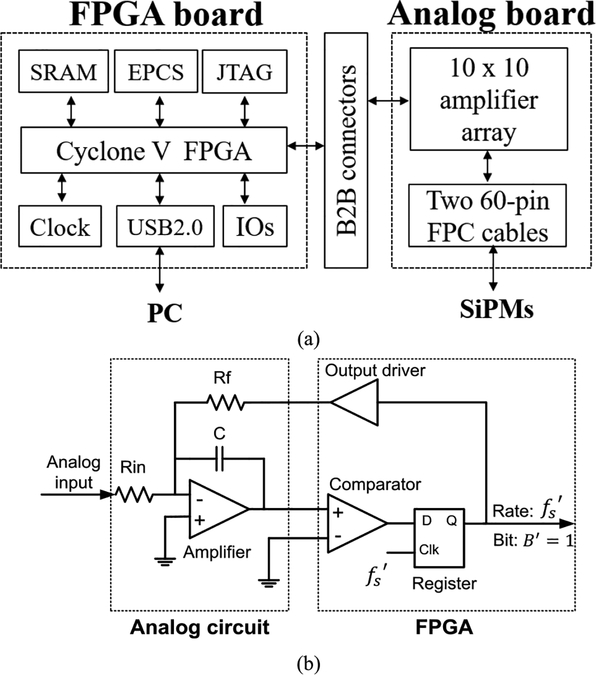
Fig. 1(a) shows the hardware configuration. A 100-channel Pico-PET electronics system consists of an FPGA board and an analog board. The FPGA board has: a low-cost FPGA (Intel Cyclone VE 5CEBA7); a 67-Mb EPCS flash memory; a 16-Mb synchronous dynamic random-access memory; 10 pairs of low-voltage differential signaling (LVDS) input output ports for clock distribution, synchronization, command communication, and list mode data transmission; a joint test action group port for on-line system debugging; an onboard 50-MHz local clock; and a micro universal serial bus (USB) 2.0 port (data rate: ~40 Mb/s) for plug-and-play event data communications from/to a host device such as a computer. The 50-MHz local clock was fed into the phase-locked loop in the FPGA to generate a 1-GHz system clock.
Fig. 1.
(a) Pico-PET electronics system, (b) First-order, 1-bit oversampled delta-sigma ADC using an FPGA.
The Pico-PET electronics deploys four 1.25G LVDS transceivers to enable data and command communications between modules. In addition, two low-voltage positive emitter-coupled logic (LVPECL) input ports and two LVPECL output ports are reserved for receiving and transmitting the global clocks and the signal for global synchronizations. Thus, multiple Pico-PET electronics modules can be conveniently scaled up to construct large-scale systems with different network topologies, such as tree or daisy chain.
The analog board consists of 100 low-power operational amplifiers and two 60-pin flexible printed circuit cables to connect to photosensors. The amplifiers were configured as shown in Fig. 1(b) to implement 1-bit over sampled delta-sigma ADCs [28]–[30]. Note that the comparator and the driver were implemented using a digital LVDS input port and a digital TTL output port from the FPGA [28], [29], respectively. Thus, the Pico-PET system only requires one amplifier, one capacitor, and two resistors per readout channel.
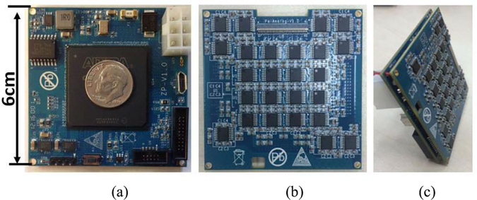
Fig. 2 shows pictures of the custom-designed FPGA board, the analog board, and the assembled 100-channel Pico-PET electronics module. The size of both boards is 6 cm × 6 cm. They are connected together with three board-to-board connectors. The size of the assembled module is 6 cm × 6 cm 0.8 cm.
Fig. 2.
Pictures of (a) custom-designed FPGA board, (b) custom-designed analog board, and (c) assembled 100-channel Pico-PET electronics module.
B. Firmware Configuration
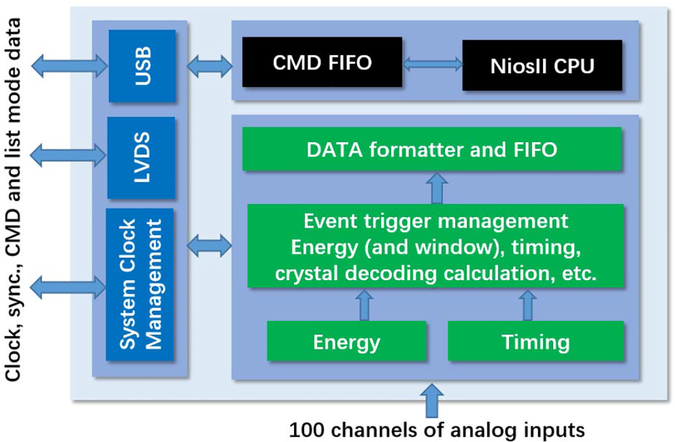
Fig. 3 shows the firmware framework for the Pico-PET system. The internal functional blocks are grouped into three categories: 1) event data processing blocks (green) read data from analog input and generate list mode data; 2) command blocks (black) process the commands for the system settings and calibrations; and 3) communication blocks (blue) provide digital data communication services for the system. Note that the event data processing blocks measure both the energy and time of a single event. The time measurements involve high-precision FPGA-based TDCs [31], [32]. This, however, is beyond the scope of this paper.
Fig. 3.
Firmware framework of the Pico-PET system.
C. Experimental Settings
Six experiments were conducted to evaluate the system’s performance and assess its unique features. The experimental settings are described in detail in the following. All the experiments were performed at room temperature (about 21 °C).
1). DC Current Measurements:
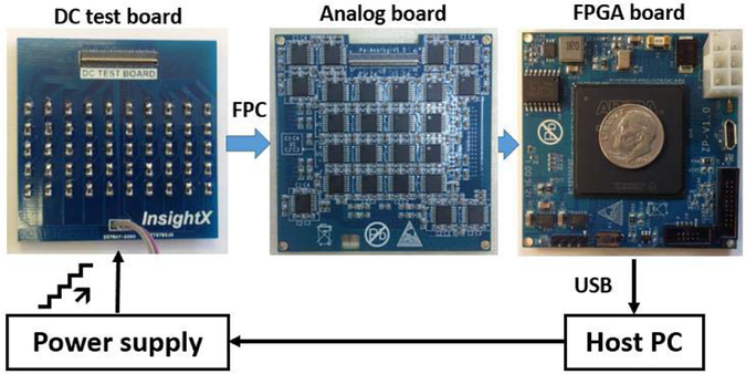
A simple direct current testing board (shown in Fig. 4) was designed and manufactured to characterize the performance of the 100-channel 1-bit oversampled delta-sigma ADCs in the Pico-PET system. The test board consisted of 100 1-MΩ resistors. A dc power supply was controlled by a host PC to provide output voltage at 0.001 V per step to generate dc currents ranging from 1 to 3000 nA. The outputs of the 1-bit registers in the FPGA were summed for 5 s for each step (N5). The dc currents (Im) were calculated as [28]
| (1) |
where Vf is the voltage (2.5 V) when the FPGA TTL output is “1.” Rf is the value of the feedback resistor (5 kΩ). f is the clock frequency (1 GHz).
Fig. 4.
Experimental settings for the dc current measurements.
In this experiment, all 100 dc current channels were measured simultaneously and transferred to the host PC via a USB 2.0 port. The transfer function between the input current (Iin) and the calculated current (Im) was then derived and analyzed. A simple linear model was used to assess the linearity of the transfer function
| (2) |
where k and I0 are the slope and offset, respectively.
2). SiPM V-I Curve Measurements:
The dark current generated in a SiPM is the product of thermally induced dark pulses, afterpulses, and crosstalk. It is temperature and bias voltage dependent [33], [34]. Many applications need the breakdown voltages [35] and gains [36] of individual SiPMs to be characterized. Traditionally, this is done by measuring one by one the dark current of single SiPMs with different voltages (called the V-I curve) [37], [38].
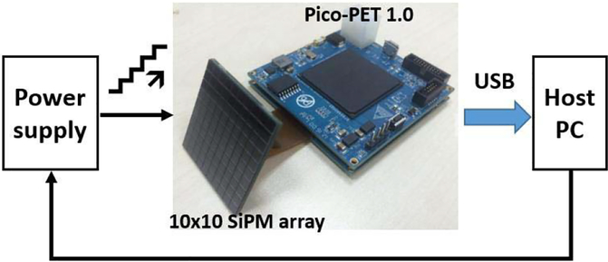
Six 10 × 10 SiPM arrays (MicroFC30035, SensL Inc.) were designed and manufactured in-house to assess the capacity of the 100-channel Pico-PET electronics with SiPM V-I curve measurements. The size of the individual SiPMs and the 10 × 10 arrays were 3 mm × 3 mm and 30 mm × 30 mm, respectively. As shown in Fig. 5, the SiPM arrays were powered by a dc power supply that was controlled by a host PC to output voltages from 20 to 30 V, with a step of 0.1 V. Like the dc current experiments, the outputs of all the 1-bit registers in the FPGA were summed simultaneously for 5 s for each step and transferred to the host PC via a USB 2.0 port. The dark current for each step was calculated using (1) to derive the V-I curve. The breakdown voltage (Vbr) and the dark current at Vbr + 2.5 V for 600 SiPMs in all six arrays were calculated and compared to the values provided by the SiPM vendor.
Fig. 5.
Experimental settings for the SiPM V-I curve measurements.
3). Energy of Test Pulses:
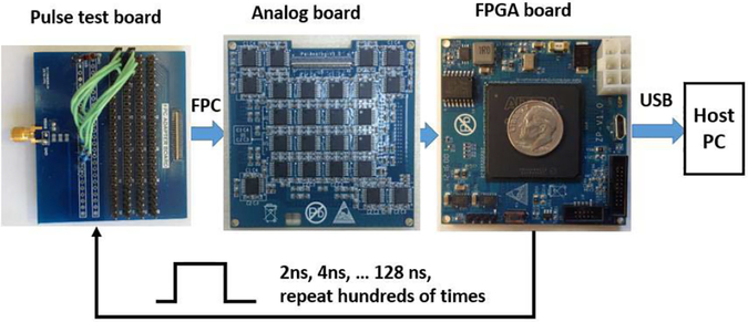
An important task for the front-end electronics in a nuclear imaging system is to measure the energy of gamma events. This is accomplished using the amplitudes and/or durations of electronic pulses. A simple test pulse board was fabricated to test the ability of the 100-channel Pico-PET electronics to measure the energy of input pulses. As shown in Fig. 6, the FPGA boards generated test pulses with widths ranging from 2to 128 ns at 2-ns steps. These were fed to the analog board. The FPGA was programmed to calculate the energy of all the input pulses by summing the 1-bit digital output from the registers. The calculated energies were transferred to the host PC via the USB 2.0 data interface. The transfer functions between the widths and the energy measurements of the input pulses were derived for all 100 channels. Note that all the test pulses had the same amplitude. Thus, the energy measurements can be expected to be proportional to the widths of the pulses.
Fig. 6.
Settings for the test pulse experiments.
The pulse experiments were repeated 200× to characterize repeatability and uniformity across 100 channels of energy measurements. The scatter plots of the pulse widths versus the calculated energies were derived and fit using linear models for all 100 channels
| (3) |
where E is the calculated energies and PW is the width of the input pulses, k and b are the slope and offset, respectively. The least significant bits (LSBs) of the calculated energy E are equivalent to electric charge
| (4) |
where Vf = 2.5 V, Rf = 5 kΩ, and f = 1 GHz. Therefore, QLSB = 0.5 pC.
The scatter plot was then subtracted using the fitted model to show the variation in the energy calculations. The mean and standard deviation (STD) of the 100 slopes k and intercepts b were calculated and compared.
4). One-to-One Coupled Detector:
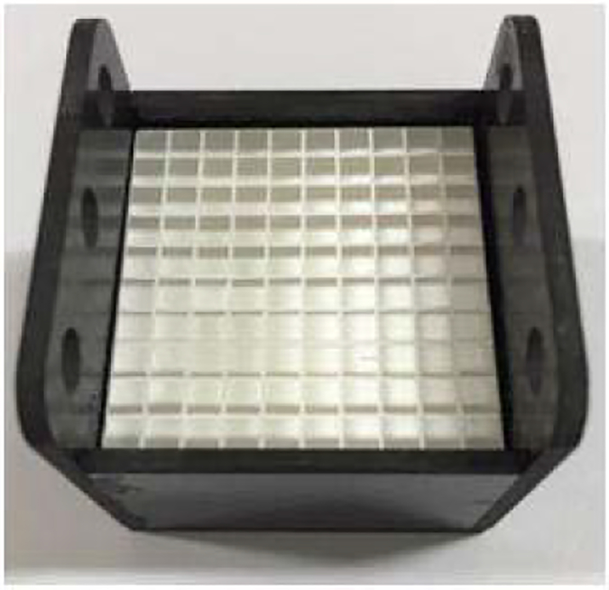
A PET detector was constructed to assess the performance of the 100-channel Pico-PET system when measuring gamma energy. The detector (see Fig. 7) consisted of a 10 × 10 array of 3 mm × 3 mm × 20 mm Lutetium-Yttrium Oxyorthosilicate (LYSO) scintillator crystals and a 10 × 10 MicroFC30035 SiPM array. The 10 × 10 scintillating crystal array was one-to-one air coupled with the 10 × 10 MicroFC30035 SiPM array (bias voltage: 27.5 V). The detector was mounted in a light-tight encasement fabricated out of carbon fiber materials and a 22Na source (20 μCi) was shone on it. The FPGA was programmed to automatically perform event triggering, energy calculation, and list-mode event data generation for all of the individual SiPMs independently. The event data were transmitted to the host PC via the USB 2.0 port in real time. The energy spectra, photopeaks, and energy resolutions of all 100 individual crystals were measured and compared. There was no need to decode the individual crystals because they were one-to-one coupled with the individual SiPMs.
Fig. 7.
10 × 10 array of 3 mm × 3 mm × 20 mm LYSO scintillator crystals for the one-to-one coupled detector experiments.
5). Crystal Decoding Performance:
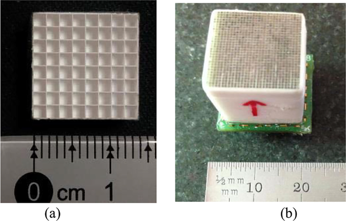
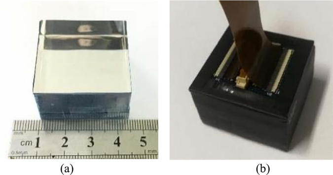
Two detector modules were constructed with SiPMs and crystals of different sizes to assess Pico-PET’s crystal decoding performance and ability to read out from different types of SiPMs. The first module [Fig. 8(a)] was constructed with an 8 × 8 array of 1.5 mm × 1.5 mm × 5 mm LYSO scintillator crystals air coupled to a part (4 × 4) of the 10 × 10 MicroFC30035 SiPM array. The surfaces of the individual SiPMs were protected by a glass layer of 0.35 mm in thickness. There is an air gap about 0.5 mm in thickness between the LYSO array and the surface of the SiPM array. The protective glasses and the air gap act together as the light guide to allow the light sharing between the SiPMs. The bias voltage of the SiPMs was set to 27.5 V. The FPGA was programmed to cluster 16 channels for event triggering, energy calculation, and list-mode event data generation.
Fig. 8.
(a) 8 × 8 array of 1.5 mm × 1.5 mm × 5 mm LYSO crystals. (b) 30 × 30 array of 0.445 mm × 0.445 mm × 20 mm LYSO crystals.
The second detector [Fig. 8(b)] was constructed with a 30× 30 array of very fine 0.445 mm × 0.445 mm × 20 mm LYSO scintillator crystals air coupled to a 2 × 2 array of 7.75 mm × 7.75 mm linearly graded SiPMs (LG-SiPM, developed by Fondazione Bruno Kessler) [39], [40]. The 0.445-mm crystal pitch is the finest currently available. The bias voltage of the LG-SiPMs was set to 35 V. The LG SiPM implements the conventional resistor-based multiplexing network circuit inside the SiPM pixel. The event signal is split into four channels. Thus, every LG-SiPM output four channels of signals. Only four channels from one LG-SiPM were connected to the 100-channel Pico-PET electronics in this experiment. The energy measured from all four channels was added to generate valid event triggering, rather than triggering on four channels individually. The FPGA was programmed to cluster four channels for event triggering, energy calculation, and list-mode event data generation.
In this experiment, a 22Na source (20 μCi) was shone on the detectors and the event data were sent to the host PC via the USB 2.0 port in real time. Crystal position decoding maps were generated using the traditional anger logic method [39], [41]. The quality of the position decoding maps was assessed qualitatively using profile analysis.
6). Readout Light Distribution in a Monolithic Scintillator:
In a monolithic detector, the 3-D positions of the gamma interactions in a scintillator crystal are calculated from the distribution of scintillating photons on the surface of the crystal [15], [19], [42]–[44]. A piece of monolithic LYSO scintillating crystal (30 mm × 30 mm × 20 mm, see Fig. 9) was manufactured for this experiment to verify the ability of the Pico-PET system to read out 2-D distributions of scintillating photons. Five surfaces of the monolithic crystal were wrapped with a Vikuiti enhanced specular reflector (ESR). The last surface was air coupled directly to the 10 × 10 MicroFC30035 SiPM array. The bias voltage of the SiPMs was set to 30 V. As before, a 22Na source (20 μCi) was shone on the detector. The FPGA was programmed to cluster all 100 channels for event triggering, energy calculation, and list-mode event data generation. All 100 channels of energy readouts of valid gamma events were transmitted to the host PC simultaneously. The typical measurements for the 2-D light distributions were captured and reviewed.
Fig. 9.
(a) 30 mm × 30 mm × 20 mm monolithic LYSO scintillating crystal, with five surfaces wrapped in Vikuiti ESR. (b) Monolithic LYSO crystal was air coupled to the 10 × 10 MicroFC30035 SiPM array and mounted in a light-tight encasement manufactured out of black carbon fiber.
III. Results
A. DC Current Measurements
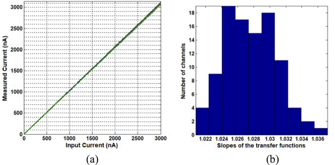
Fig. 10(a) shows the transfer functions between the input dc currents and the measurements from all 100 channels. The 100 transfer functions are identical and have excellent linearity (R2 = 0.9999). Fig. 10(b) shows the slope distribution for the 100 transfer functions. The mean and the STD of the 100 slopes were 1.0276 and 0.0033, respectively. The uniformity over the 100 channels was excellent. Note that the measured currents were slightly larger (2.76%) than the true input dc current because the FPGA TTL voltage was slightly lower than the expected 2.5 V. This is something that can easily be calibrated when necessary.
Fig. 10.
(a) Plots of the 100 transfer functions of the input and measured dc currents. The dc currents ranged from 1 nA to 3 μ A with a step of 1 nA. (b) Slope distributions for the 100 transfer functions.
B. SiPM V-I Curve Measurements
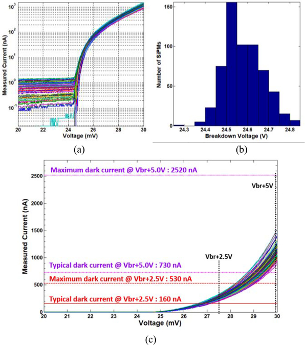
Fig. 11(a) shows the measured V-I curves from the six 10 × 10 MicroFC30035 SiPM arrays. The 100-channel Pico-PET system was able to measure dark currents as low as about 100 pA at the bias voltage of 20 V. The distribution of the measured breakdown voltages of the 600 SiPMs (mean ± STD: 24.6 V ± 0.089 V) is shown in Fig. 11(b). The measurements agree well with the values provided in the SiPM datasheet (typical value: 24.5 V; minimum value: 24.25 V, and maximum value: 24.75 V). Fig. 11(c) compares the measured dark currents with the values given in the datasheet. The range of the measured dark currents at overvoltages of 2.5 and 5.0 V was 200–300 nA and 900–1500 nA, respectively. These values agree reasonably well with the maximum dark currents listed in the datasheet (530 nA at 2.5 V and 2520 nA at 5V).
Fig. 11.
Results of the SiPM V-I curve experiments, (a) Log-linear plot of the V-I curves for 600 SiPMs measured with the 100-channel Pico-PET system, (b) Distribution of the measured breakdown voltages of the 600 SiPMs (mean ± STD: 24.6 V ± 0.089 V). (c) Linear scale plot of the 600 V-I curves. The typical and maximum dark currents provided by the SiPM vendor are marked in the plot with horizontal lines.
C. Energy of the Test Pulses
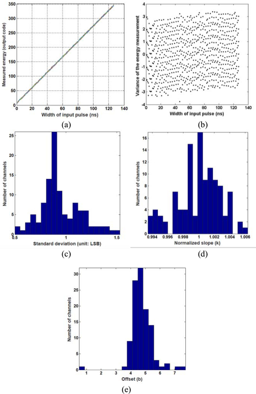
Fig. 12(a) shows the 200 plots of the input pulse widths versus the energies measured from a typical channel. Again, the 200 plots are identical and have excellent linearity. Variation in the 200 repeated measurements [see Fig. 12(b)] is smaller than ±4 LSB. As calculated in (4), an LSB is equivalent to 0.5-pC electric charge. The STD of the variations is 1.36 LSB (0.68 pC). The distribution of the STDs of the variations of all 100 channels [Fig. 12(c)] ranges from 0.5 to 1.5 LSB or 0.25 to 0.75 pC. Fig. 12(d) and (e) shows the distribution of the normalized slopes k and offsets b for the 100 linear transfer functions. The results show that the 100 channels have excellent gain (slope) uniformity (difference < ±0.5%). The maximum and average offsets in the energy measurements are 4.5 LSB (2.25 pC) and 7.7 LSB (3.85 pC), respectively. These quantitative results confirm Pico-PET’s excellent accuracy, linearity, repeatability, and uniformity for pulse energy measurement.
Fig. 12.
Results of the test pulse experiments, (a) 200 curves of the input pulse widths versus the energies measured from one typical channel, (b) Variation in the measured energies of the typical channel in 200 repeated tests, (c) Distribution of the STDs of the energy measurements for the 100 channels. The distribution of (d) normalized slope k and (e) offset b of the linear transfer functions of the input pulse widths versus the measured energies. A LSB is equivalent to 0.5-pC electric charge.
D. One-to-One Coupled Detector
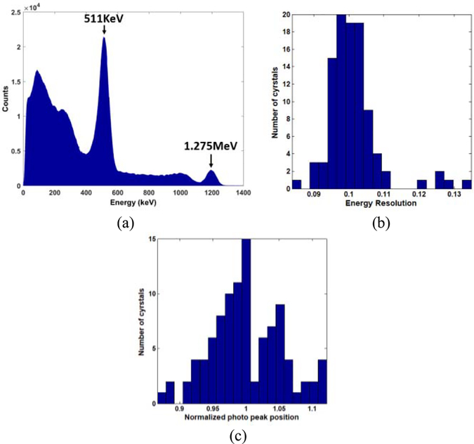
Fig. 13(a) shows a typical energy spectrum for 22Na measured by a Pico-PET channel. The spectrum displays clearly and accurately both the 511-keV annihilation photopeak of the positron emitter and the photopeak of the 1.275-MeV gamma ray. An excellent full-width half-maximum (FWHM) energy resolution (10.5%) was measured on the 511-keV photopeak. Fig. 13(b) shows the distribution of the energy resolutions for all 100 discrete crystals in the 10 × 10 array. The mean and STD of the energy resolutions were 10.0% and 0.7%, respectively. Fig. 13(c) shows that the normalized position of the 511-keV photopeak varied in the range of 0.87 to 1.11, with an STD of 0.054. These results indicate that the 100-channel Pico-PET system is able to measure the energy spectrum of gamma events with high levels of accuracy, linearity, and uniformity.
Fig. 13.
(a) Typical energy spectrum, (b) Distribution of the energy resolution for the 100 discrete crystals, (c) Distribution of the normalized position of the 511-keV photopeak.
E. Crystal Decoding Performance
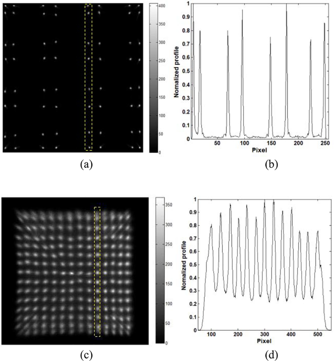
Fig. 14(a) and (b) shows the crystal decoding map and a profile of the 8 × 8 array of 1.5 mm × 1.5 mm × 5 mm LYSO crystals. All of the 1.5-mm crystals are distinctly separate from each other in the decoding map. The profile analysis shows that all of the peaks have exceptional peak-to-village ratios (PTVRs), being all larger than 20.
Fig. 14.
(a) Crystal decoding map for the 8 × 8 array of 1.5 mm × 1.5 mm × 5 mm LYSO crystals, (b) Profile of the crystal column marked by the yellow dashed box in decoding map a), (c) Crystal decoding map for the 30 × 30 array of 0.445 mm × 0.445 mm × 20 mm LYSO crystals, (d) Profile of the crystal column marked by the yellow dashed box in decoding map c).
Fig. 14(c) and (d) shows the crystal decoding map and a profile of the 30 × 30 array of 0.445 mm × 0.445 mm × 20 mm LYSO crystals. The decoding map covers one-quarter of the discrete crystals of the 30 × 30 array because only one LG-SiPM (four channels) was connected to the Pico-PET system. All the 0.445-mm crystals, except for some on the edges, are distinctly separate from each other in the decoding map. The profile analysis shows that here too, the peaks have excellent PTVRs (mean =b STD: 3.6 =b 0.51). These results indicate that the Pico-PET system has an excellent decoding ability that matches or outperforms most other readout electronics currently used in the research and industrial community [39], [45], [46].
F. Readout Light Distribution in a Monolithic Scintillator
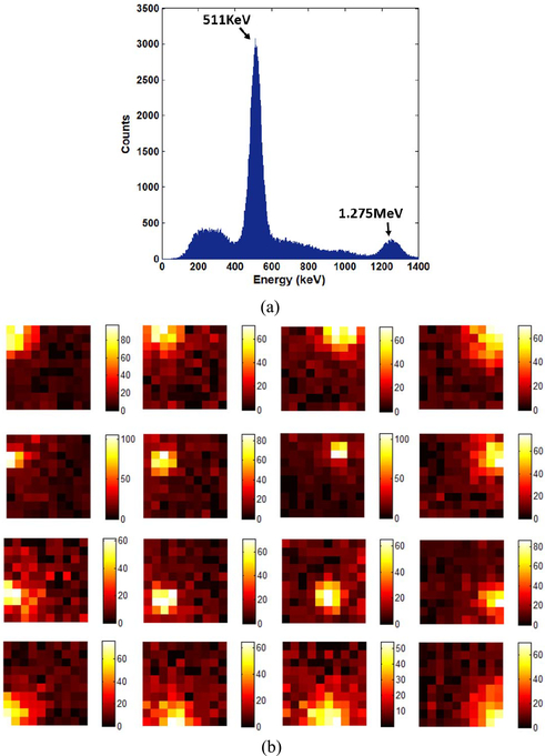
Fig. 15(a) shows a typical energy spectrum for 22Na measured with the monolithic LYSO crystal and 100-channel Pico-PET system. A good FWHM energy resolution (12.9%) was measured on the 511-keV photopeak. Fig. 15(b) shows 16 typical maps of the distribution of the scintillating photons generated by single gamma photons interacting with different parts of the monolithic scintillator. These results demonstrate the outstanding capacity of the Pico-PET system to read out 2-D distributions of photons.
Fig. 15.
(a) Typical energy spectrum, (b) 16 typical maps of light distribution representative of single scintillation events measured by the 100-channel Pico-PET system.
IV. Discussion
SiPMs are widely used in light detection and ranging, automated test equipment, high-energy physics experiments, and nuclear medical imaging systems. A fundamental technical obstacle to applying large-scale SiPM arrays is the challenge of reading out a large number of detection channels, from hundreds to thousands or more. Apart from the cost, it is both difficult and not especially practical to use conventional electronics with discrete components to read out hundreds or thousands of channels. The bulky size of the electronics alone would prevent the connection of the individual SiPMs inside a compact array or packing the detectors closely together. In 2016, a group at Lawrence Berkeley National Laboratory (USA) developed and released a general purpose open-source high-performance electronics system for nuclear imaging, called OpenPET electronics [45]–[47]. OpenPET adapted conventional front-end electronics using a high-performance ADC. A fully installed OpenPET module, consisting of a motherboard, eight analog boards (16 channels per board. 128 channels in total), and some debugging boards, is 30 cm × 30 cm × 44 cm in size, costs about U.S. $30000, and consumes 100 W of power.
In this paper, we have successfully developed a novel 100-channel Pico-PET electronics system based on 1-bit sigma-delta modulation and an FPGA, with off-the-shelf low-cost components. Unlike the 128-channel OpenPET system, the Pico-PET system only requires one single FPGA board and one analog board. Almost all aspects of the front-end readout electronics, including signal splitting, event triggering, ADCs, and TDCs, are implemented inside the low-cost programmable FPGA. Thus, the cost (~U.S. $800), power consumption (< 3W), and size (6 cm × 6 cm × 0.8 cm) of the Pico-PET system are significantly lower or smaller than they are for OpenPET.
Six different experiments were conducted to evaluate the performance of the Pico-PET system and assess its unique features. The experiments relating to dc current measurement confirmed the system’s ability to measure 100 channels of dc current accurately, linearly, and uniformly. SiPM V-I curve measurements revealed its unique capacity to capture the V-I curves and measure the breakdown voltages and dark currents of 100 SiPMs accurately, uniformly, and simultaneously.
Note that the temperature dependence of the breakdown voltage, dark current, and gain [48] is one of the major downsides of analog SiPM detectors. None of the current ASICs and electronics systems developed for nuclear imaging, outside of Pico-PET, can measure the V-I curves, breakdown voltages, and dark currents of multiple SiPMs simultaneously. This core feature of the Pico-PET system enables the potential to monitor and compensate for temperature dependence in the breakdown voltage, dark current, and gain of multiple SiPMs simultaneously. More specifically, the gainG(V) of a SiPM is approximately [49]
| (5) |
where V and Vbd are the bias voltage and the breakdown voltage, respectively. Cpix and q0 are the single pixel capacitance and the elementary charge, respectively. Equation (5) indicates that the gain of a SiPM is approximately proportional to the difference between the bias voltage and the temperature-sensitive breakdown voltage [50]. Thus, the differences of the gains among multiple SiPMs can be normalized conveniently by applying the calibration coefficients c = 1/(V − Vbd) for the individual SiPMs. The temperature compensation can also be implemented simply by measuring the breakdown voltages and updating the calibration coefficients periodically.
The experiments regarding pulse measurements showed that the Pico-PET system is able to measure the energies of 100 channels of pulse signals with excellent accuracy, linearity, and uniformity. As expected, accurate energy spectra and outstanding energy resolution were achieved in experiments using a one-to-one coupled detector. These results indicate that Pico-PET is a powerful tool for applications, such as high-energy physics experiments and nuclear imaging system, where the accurate measurement of energy spectra are required.
Generally, there are two types of gamma detectors for nuclear medical imaging. The first uses discrete crystal arrays, where the locations of gamma interactions are decoded using lookup tables generated by segmenting the position decoding map [51], [52]. The second type is constructed with one piece of monolithic crystal. The locations of the gamma interactions here are calculated according to the distribution of scintillating photons measured on the surfaces of the crystal [15], [19], [42]–[44]. The experiments using detectors constructed with very fine discrete crystal arrays (0.445 mm) and the monolithic crystal demonstrated the extraordinary capacity of the Pico-PET system for both discrete crystal decoding and the measurement of light distribution. The experiments also demonstrated Pico-PET’s excellent flexibility when reading out SiPMs provided by different manufacturers (SensL’s MicroFC30035 and Fondazione Bruno Kessler’s LG-SiPM), and when clustering different numbers of channels (1, 4, 16, and 100 for the four detectors shown in Figs. 7, 8(b) and (a), and 9, respectively) for event triggering and energy calculation.
The dead time for processing an ideal short pulse input is determined by the frequency of the sampling clock (f) and dynamic range (DR) requirements of the energy measurement
| (6) |
For example, the dead time is 512 ns when DR = 9 bits and f = 1 GHz. That indicates that the maximum rate tolerance is about 2 MHz per channel in an ideal situation.
The timing performance is an essential performance of the readout electronics for nuclear imaging. In the current version of the Pico-PET electronics, the timing measurements are implemented using digital counters in the FPGA. The intrinsic timing resolutions are determined by the clock frequencies. A 1-ns timing resolution was achieved naturally when a 1-GHz system clock was adapted in the 100-channel 1-bit oversampled delta-sigma ADCs. That meets the requirements of many applications, such as the preclinical PET and clinical non-time-of-flight (TOF) PET.
However, a much better timing resolution is requested for the next generation of TOF PET [53], [54]. A low-cost, high-performance FPGA-based TDC [named nonuniform multi-phase (NUMP) TDC] has been developed [32]. Four channels of NUMP TDCs have been implemented and an excellent (2.3 ps) timing resolution was measured with testing pulses. As a next step, we will implement 100 channels of FPGA-based TDCs in the Pico-PET electronics and perform experimental studies to evaluate the timing performances.
The Pico-PET electronics transfers the event data to the host device using a micro USB 2.0 port. The full-speed data combination rate was measured to be about 40 Mb/s. The size of the data package was fixed to 32 bits, while the format and length of the valid event data are flexible and vary in different applications. For example, 32-bit event data, including 1 flag bit, 11 bits of energy, 12 bits of time stamp, and 8 bits of channel ID, were transferred to the host PC in the experiments with the one-to-one coupled detector. The maximum data transfer rate was about 1.25-M counts per second. In the experiments with a monolithic scintillator, 10032-bit data packages were occupied to transfer the light distribution measured from 100 channels for every valid event. Thus, the maximum data transfer rate was about 12.5-K counts per second.
V. Conclusion
Detector readout for numerous SiPM array channels is a fundamental technical problem that limits the potential for developing advanced nuclear imaging technology. A Pico-PET electronics system based on novel 1-bit Σ-Δ modulation and an FPGA was developed to solve this long-standing problem. The cost, power consumption, and size of the Pico-PET system are about 30 × cheaper, 26 × lower, and l000× smaller, respectively, than OpenPET, which is a commonly used open-source high-performance system for nuclear medical imaging. The Pico-PET system has some unique, essential, and sought-after features that are not available in any other ASICs and electronics systems for nuclear imaging. These include an ability to measure V-I curves, breakdown voltages, and dark currents for 100 SiPMs accurately, simultaneously, and in real time. Furthermore, the flexibility afforded by using an FPGA enables multiple channel clustering and intelligent triggering for different detector designs.
Pico-PET will make it much easier for small academic and industrial research groups to come up with new innovative ideas and approaches [55], [56]. This will significantly accelerate and expand the progress of research, technology, and application development in the field of nuclear imaging.
Acknowledgments
This work was supported in part by the National Natural Science Foundation of China under Grant 51627807, in part by the National Institutes of Health, and in part by the National Institute of Biomedical Imaging and Bioengineering under Grant R01EB006085. The Associate Editor coordinating the review process was Branislav Djokic.
Biographies

Zhixiang Zhao (S’16) was born in Zhumadian, Henan, China, in 1993. He received the B.S. degree in biomedical engineering from the University of Shanghai for Science and Technology, Shanghai, China, in 2015. He is currently pursuing the Ph.D. degree with the School of Biomedical Engineering, Shanghai Jiao Tong University, Shanghai.
He is currently a Visiting Student with the Molecular Biophysics and Integrated Bioimaging Division, Lawrence Berkeley National Laboratory, Berkeley, CA, USA. His current research interests include hardware and software designs of high-performance positron emission tomography systems.

Siwei Xie (S’17) received the B.S. degree in mechanical engineering from the Wuhan University of Technology, Wuhan, China, in 2015. He is currently pursuing the Ph.D. degree with the School of Mechanical Science and Engineering, Huazhong University of Science and Technology, Wuhan.
He is currently a Visiting Student with the Department of Molecular Biophysics and Integrated Bioimaging, Lawrence Berkeley National Laboratory, Berkeley, CA, USA. His current research interests include nuclear medicine and functional imaging.

Xi Zhang (S’17) received the B.S. degree in mechanical design manufacture and automation from the Huazhong University of Science and Technology, Wuhan, China, in 2016, where he is currently pursuing the master’s degree with the Ultra Precision and Intelligent Manufacturing Laboratory, School of Mechanical Science and Engineering.
His current research interests include positron emission tomography detector design.

Jingwu Yang received the B.S. degree in mechanical design manufacturing and automation from the Huazhong University of Science and Technology, Wuhan, China, in 2017, where he is currently pursuing the master’s degree with the School of Mechanical Science and Engineering.
He is currently a Visiting Student with the Department of Molecular Biophysics and Integrated Bioimaging, Lawrence Berkeley National Laboratory, Berkeley, CA, USA. His current research interests include high-performance positron emission tomography system design.

Jianfeng Xu received the B.S. degree from the School of Mechanical Science and Engineering, Huazhong University of Science and Technology, Wuhan, China, in 2001, and the Ph.D. degree in mechanical engineering from the University of California at San Diego, San Diego, CA, USA, in 2008.
Since 2012, he has been a Professor with the School of Mechanical Science and Engineering, Huazhong University of Science and Technology, where he is currently involved in the development of precision engineering, and instrumentation of nuclear medicine and functional imaging.

Qiu Huang received the Ph.D. degree in electrical engineering from the University of Utah, Salt Lake City, UT, USA.
She is currently a Research Professor with the School of Biomedical Engineering and an Adjunct Research Professor with the Department of Nuclear Medicine, Ruijin Hospital, School of Medicine, Shanghai Jiao Tong University, Shanghai, China. Her current research interests include designs of instrumentation and algorithm in nuclear medicine imaging.

Qiyu Peng (M’04) received the Ph.D. degree in biomedical engineering from Tsinghua University, Beijing, China, in 2003.
He is currently a Career Scientist with the Department of Molecular Biophysics and Integrated Bioimaging, Lawrence Berkeley National Laboratory, Berkeley, CA, USA. His current research interests include nuclear medicine and functional imaging, biomedical ultrasound imaging, wireless biomonitoring, biorobotics, and studies on the mechanism and rehabilitation of neurological impairments including stroke, spinal cord injury, and urinary continence.
Footnotes
Color versions of one or more of the figures in this paper are available online at http://ieeexplore.ieee.org.
Contributor Information
Zhixiang Zhao, School of Biomedical Engineering, Shanghai Jiao Tong University, Shanghai 200025, China..
Qiu Huang, School of Biomedical Engineering, Shanghai Jiao Tong University, Shanghai 200025, China..
Jianfeng Xu, State Key Laboratory of Digital Manufacturing Equipment and Technology, School of Mechanical Science and Engineering, Huazhong University of Science and Technology, Wuhan 430074, China..
Qiyu Peng, Department of Molecular Biophysics and Integrated Bioimaging, Lawrence Berkeley National Laboratory, Berkeley, CA 94720 USA..
References
- [1].Buzhan P et al. , “Silicon photomultiplier and its possible applications,” Nucl. Instrum. Methods Phys. Res. A, Accel. Spectrom. Detect. Assoc. Equip, vol. 504, nos. 1–3, pp. 48–52, 2003. [Google Scholar]
- [2].Buzhan P et al. , “Large area silicon photomultipliers: Performance and applications,” Nucl. Instrum. Methods Phys. Res. A, Accel. Spectrom. Detect. Assoc. Equip, vol. 567, no. 1, pp. 78–82, November 2006. [Google Scholar]
- [3].Dolgoshein B, “Silicon photomultipliers in particle physics: Possibilities and limitations,” in Innovative Detectors for Supercolliders, vol. 25 Singapore: World Scientific, 2004, pp. 442–456. [Google Scholar]
- [4].Roncali E and Cherry SR, “Application of silicon photomultipliers to positron emission tomography,” Ann. Biomed. Eng, vol. 39, no. 4, pp. 1358–1377, 2011. [DOI] [PMC free article] [PubMed] [Google Scholar]
- [5].Wu Y et al. , “PET performance evaluation of an MR-compatible PET insert,” IEEE Trans. Nucl. Sei, vol. 56, no. 3, pp. 574–580, June 2009. [DOI] [PMC free article] [PubMed] [Google Scholar]
- [6].Goertzen AL et al. , “Design and performance of a resistor multiplexing readout circuit for a SiPM detector,” IEEE Trans. Nucl. Sei, vol. 60, no. 3, pp. 1541–1549, June 2013. [Google Scholar]
- [7].Janecek M et al. , “A high-speed multi-channel readout for SSPM arrays,” IEEE Trans. Nucl. Sei, vol. 59, no. 1, pp. 13–18, February 2012. [Google Scholar]
- [8].Kim KB, Choi Y, Jung J, Lee S, Choe H-J, and Leem HT, “Analog and digital signal processing method using multi-time-over-threshold and FPGA for PET,” Med. Phys, vol. 45, no. 9, pp. 4104–4111, September 2018. [DOI] [PubMed] [Google Scholar]
- [9].Jung J, Choi Y, Kim KB, Lee S, and Choe HJ, “An improved time over threshold method using bipolar signals,” Phys. Med. Biol, vol. 63, no. 13, p. 135002, June 25 2018. [DOI] [PubMed] [Google Scholar]
- [10].Chang CM, Cates JW, and Levin CS, “Time-over-threshold for pulse shape discrimination in a time-of-flight phoswich PET detector,” Phys. Med. Biol, vol. 62, no. 1, pp. 258–271, January 7 2017. [DOI] [PMC free article] [PubMed] [Google Scholar]
- [11].Kuang Z et al. , “Development of depth encoding small animal PET detectors using dual-ended readout of pixelated scintillator arrays with SiPMs,” Med. Phys, vol. 45, no. 2, pp. 613–621, February 2018. [DOI] [PubMed] [Google Scholar]
- [12].Mohammadi A, Yoshida E, Nishikido F, Nitta M, Shimizu K, and Sakai T, “Development of a dual-ended readout detector with segmented crystal bars made using a subsurface laser engraving technique,” Phys. Med. Biol, vol. 63, no. 2, p. 025019, January 2018. [DOI] [PubMed] [Google Scholar]
- [13].Borghi G, Tabacchini V, Bakker R, and Schaart DR, “Sub-3 mm, near-200 ps TOF/DOI-PET imaging with monolithic scintillator detectors in a 70 cm diameter tomographic setup,” Phys. Med. Biol, vol. 63, no. 15, p. 155006, July 27 2018. [DOI] [PubMed] [Google Scholar]
- [14].Zhang X et al. , “Performance of a SiPM based semi-monolithic scintillator PET detector,” Phys. Med. Biol, vol. 62, no. 19, pp. 7889–7904, September 2017. [DOI] [PubMed] [Google Scholar]
- [15].Etxebeste A, Barrio J, Muñoz E, Oliver JF, Solaz C, and Llosá G, “3D position determination in monolithic crystals coupled to SiPMs for PET,” Phys. Med. Biol, vol. 61, no. 10, pp. 3914–3934, May 2016. [DOI] [PubMed] [Google Scholar]
- [16].Di Francesco A et al. , “TOFPET2: A high-performance ASIC for time and amplitude measurements of SiPM signals in time-of-flight applications,” J. Instrum, vol. 11, p. C03042, March 2016. [Google Scholar]
- [17].Rolo MD et al. , “TOFPET ASIC for PET applications,” J. Instrum, vol. 8, p. C02050, February 2013. [Google Scholar]
- [18].Cho M et al. , “A design of a valid signal selecting and position decoding ASIC for PET using silicon photomultipliers,” J. Instrum, vol. 12, p. C01089, January 2017. [Google Scholar]
- [19].Aguilar A et al. , “Pilot tests of a PET detector using the TOF-PET ASIC based on monolithic crystals and SiPMs,” J. Instrum, vol. 11, p. C12033, December 2016. [Google Scholar]
- [20].Zhu X, Deng Z, Chen Y, Liu Y, and Liu Y, “Development of a 64-channel readout ASIC for an 8 × 8 SSPM array for PET and TOF-PET applications,” IEEE Trans. Nucl. Sei, vol. 63, no. 3, pp. 1327–1334, June 2016. [Google Scholar]
- [21].Ahmad S et al. , “Triroc: A multi-channel SiPM read-out ASIC for PET/PET-ToF application,” IEEE Trans. Nucl. Sei, vol. 62, no. 3, pp. 664–668, June 2015. [Google Scholar]
- [22].Ambe T, Ikeda H, Kataoka J, Matsuda H, and Kato T, “Development and evaluation of an ultra-fast ASIC for future PET scanners using TOF-capable MPPC array detectors,” Nucl. Instrum. Methods Phys. Res. A, Accel. Spectrom. Detect. Assoc. Equip, vol. Ill, pp. 66–73, January 2015. [Google Scholar]
- [23].Piemonte C, Gola A, Tarolli A, Fisher P, Ritzert M, and Schulz V, “Performance of FBK SiPMs coupled to PETA3 read-out ASIC for PET application,” Nucl. Instrum. Methods Phys. Res. A, Accel. Spectrom. Detect. Assoc. Equip, vol. 718, pp. 345–346, August 2013. [Google Scholar]
- [24].Matsuda H et al. , “Development of ultra-fast ASIC for future PET scanners using TOF-capable MPPC detectors,” Nucl. Instrum. Methods Phys. Res. A, Accel. Spectrom. Detect. Assoc. Equip, vol. 699, pp. 211–215, January 2013. [Google Scholar]
- [25].Brunner SE, Gruber L, Hirtl A, Suzuki K, Marton J, and Schaart DR, “A comprehensive characterization of the time resolution of the philips digital photon counter,” J. Instrum, vol. 11, p. PI 1004, November 2016. [Google Scholar]
- [26].Casella C, Heller M, Joram C, and Schneider T, “A high resolution TOF-PET concept with axial geometry and digital SiPM readout,” Nucl. Instrum. Methods Phys. Res. A, Accel. Spectrom. Detect. Assoc. Equip, vol. 736, pp. 161–168, February 2014. [Google Scholar]
- [27].Degenhardt C, Zwaans B, Frach T, and de Gruyter R, “Arrays of digital Silicon Photomultipliers—Intrinsic performance and application to scintillator readout,” presented at the IEEE Nucl. Sei. Symp. Med. Imag. Conf., Knoxville, TN, USA, Oct-Nov 2010, pp. 1954–1956. [Google Scholar]
- [28].Zhao Z et al. , “A novel read-out electronics design based on 1-bit sigma-delta modulation,” IEEE Trans. Nucl. Sei, vol. 64, no. 2, pp. 820–828, February 2017. [Google Scholar]
- [29].Acero J, Navarro D, Barragan LA, Garde I, Artigas JI, and Burdio JM, “FPGA-based power measuring for induction heating appliances using sigma-delta A/D conversion,” IEEE Trans. Ind. Electron, vol. 54, no. 4, pp. 1843–1852, August 2007. [Google Scholar]
- [30].Jimenez O, Lucia O, Urriza I, Barragan LA, and Navarro D, “Design and evaluation of a low-cost high-performance ΣΔ ADC for embedded control systems in induction heating appliances,” IEEE Trans. Ind. Electron, vol. 61, no. 5, pp. 2601–2611, May 2014. [Google Scholar]
- [31].Zheng J, Cao P, Jiang D, and An Q, “Low-cost FPGA TDC with high resolution and density,” IEEE Trans. Nucl. Sei, vol. 64, no. 6, pp. 1401–1408, June 2017. [Google Scholar]
- [32].Sui T, Zhao Z, Xie S, Huang Q, Xu J, and Peng Q, “Pico-TDC: A novel FPGA-based TDC with 2.2ps RMS timing resolution,” in Proc. IEEE Nucl. Sei. Symp. Med. Imag. Conf. (NSS/MIC), Atlanta, G A, USA, November 2017. [Google Scholar]
- [33].Pagano R et al. , “Dark current in silicon photomultiplier pixels: Data and model,” IEEE Trans. Electron Devices, vol. 59, no. 9, pp. 2410–2416, September 2012. [Google Scholar]
- [34].Ramilli M, “Characterization of SiPM: Temperature dependencies,” in Proc. IEEE Nucl. Sei. Symp. Med. Imag. Conf. (Nss/Mic), vols. 1–9, October 2008, pp. 2467–2470. [Google Scholar]
- [35].Nagy F, Hegyesi G, Kalinka G, and Molnar J, “A model based DC analysis of SiPM breakdown voltages,” Nucl. Instrum. Methods Phys. Res. A, Accel. Spectrom. Detect. Assoc. Equip, vol. 849, pp. 55–59, March 2017. [Google Scholar]
- [36].Licciulli F and Marzocca C, “An active compensation system for the temperature dependence of SiPM gain,” IEEE Trans. Nucl. Sei, vol. 62, no. 1, pp. 228–235, February 2015. [Google Scholar]
- [37].Popova E, Buzhan P, Kayumov F, and Stifutkin A, “Measurement of volt-ampere characteristics of the SiPM on wafer level with setup based on the PA200 BlueRay probe station,” J. Phys., Conf. Ser, vol. 798, no. 1, p. 012215, 2018. [Google Scholar]
- [38].Otte AN, Garcia D, Nguyen T, and Purushotham D, “Characterization of three high efficiency and blue sensitive silicon photomultipliers,” Nucl. Instrum. Methods Phys. Res. A, Accel. Spectrom. Detect. Assoc. Equip, vol. 846, pp. 106–125, February 2017. [Google Scholar]
- [39].Du J et al. , “Performance of a high-resolution depth-encoding PET detector module using linearly-graded SiPM arrays,” Phys. Med. Biol, vol. 63, no. 3, p. 035035, February 2018. [DOI] [PMC free article] [PubMed] [Google Scholar]
- [40].Ferri A, Acerbi F, Gola A, Paternoster G, Piemonte C, and Zorzi N, “Characterization of linearly graded position-sensitive silicon photomultipliers,” IEEE Trans. Nucl. Sei, vol. 62, no. 3, pp. 688–693, June 2015. [DOI] [PMC free article] [PubMed] [Google Scholar]
- [41].Xie S, Chen J, Yang M, Shi H, Peng Q, and Xu J, “A γ-photon detector based on liquid light guide for whole-body PET,” J. Instrum, vol. 12, p. PI 1012, November 2017. [Google Scholar]
- [42].Borghi G, Peet BJ, Tabacchini V, and Schaart DR, “A 32 mm × 32 mm × 22 mm monolithic LYSO:Ce detector with dual-sided digital photon counter readout for ultrahigh-performance TOF-PET and TOF-PET/MRI,” Phys. Med. Biol, vol. 61, no. 13, pp. 4929–4949, July 2016. [DOI] [PubMed] [Google Scholar]
- [43].Marcinkowski R, Mollet P, Van Holen R, and Vandenberghe S, “Submillimetre DOI detector based on monolithic LYSO and digital SiPM for a dedicated small-animal PET system,” Phys. Med. Biol, vol. 61, no. 5, pp. 2196–2212, March 2016. [DOI] [PubMed] [Google Scholar]
- [44].Zhang H, Zhou R, and Yang C, “A PET detector module with monolithic crystal, single end readout, SiPM array and high depth-of-interaction resolution,” J. Instrum, vol. 11, p. P08020, August 2016. [Google Scholar]
- [45].Choong W-S, Abu-Nimeh F, Moses WW, Peng Q, Vu CQ, and Wu J-Y, “A front-end readout detector board for the OpenPET electronics system,” J. Instrum, vol. 10, p. T08002, August 2015. [DOI] [PMC free article] [PubMed] [Google Scholar]
- [46].Moses WW et al. , “OpenPET: A flexible electronics system for radiotracer imaging,” IEEE Trans. Nucl. Sei, vol. 57, no. 5, pp. 2532–2537, October 2010. [DOI] [PMC free article] [PubMed] [Google Scholar]
- [47].Abu-Nimeh FT, Ito J, Moses WW, Peng Q, and Choong W-S, “Architecture and implementation of OpenPET firmware and embedded software,” IEEE Trans. Nucl. Sei, vol. 63, no. 2, pp. 620–629, April 2016. [DOI] [PMC free article] [PubMed] [Google Scholar]
- [48].Licciulli F, Indiveri I, and Marzocca C, “A novel technique for the stabilization of SiPM gain against temperature variations,” IEEE Trans. Nucl. Sei, vol. 60, no. 2, pp. 606–611, April 2013. [Google Scholar]
- [49].Chmill V, Garutti E, Klanner R, Nitschke M, and Schwandt J, “Study of the breakdown voltage of SiPMs,” Nucl. Instrum. Methods Phys. Res. A, Accel. Spectrom. Detect. Assoc. Equip, vol. 845, pp. 56–59, February 2017. [Google Scholar]
- [50].Dinu N, Nagai A, and Para A, “Breakdown voltage and triggering probability of SiPM from IV curves at different temperatures,” Nucl. Instrum. Methods Phys. Res. A, Accel. Spectrom. Detect. Assoc. Equip, vol. 845, pp. 64–68, February 2017. [Google Scholar]
- [51].Chaudhari AJ, Joshi AA, Bowen SL, Leahy RM, Cherry SR, and Badawi RD, “Crystal identification in positron emission tomography using nonrigid registration to a Fourier-based template,” Phys. Med. Biol, vol. 53, no. 18, pp. 5011–5027, September 2008. [DOI] [PMC free article] [PubMed] [Google Scholar]
- [52].Schellenberg G, Stortz G, and Goertzen AL, “An algorithm for automatic crystal identification in pixelated scintillation detectors using thin plate splines and Gaussian mixture models,” Phys. Med. Biol, vol. 61, no. 3, pp. N90–N101, February 2016. [DOI] [PubMed] [Google Scholar]
- [53].Gundacker S, Auffray E, Pauwels K, and Lecoq P, “Measurement of intrinsic rise times for various L(Y)SO and LuAG scintillators with a general study of prompt photons to achieve 10 ps in TOF-PET,” Phys. Med. Biol, vol. 61, no. 7, pp. 2802–2837, April 2016. [DOI] [PubMed] [Google Scholar]
- [54].Lecoq P, “Pushing the limits in time-of-flight PET imaging,” IEEE Trans. Radiat. Plasma Med. Sei, vol. 1, no. 6, pp. 473–485, November 2017. [Google Scholar]
- [55].Xu J, Zhao Z, Xie S, Shi D, Huang Q, and Peng Q, “Mind-tracker PET: A wearable PET camera for brain imaging,” in Proc. IEEE Nucl. Sei. Symp. Med. Imag. Conf, Atlanta, GA, USA, November 2017. [Google Scholar]
- [56].Xie S et al. , “LOR-PET: A novel PET camera constructed with a monolithic scintillator ring,” in Proc. IEEE Nucl. Sei. Symp. Med. Imag. Conf, Atlanta, GA, USA, November 2017. [Google Scholar]


