Abstract
A new strategy to achieve large-scale, three-dimensional (3D) micro- and nanostructured surface patterns through selective electrochemical growth on monolayer colloidal crystal (MCC) templates is reported. This method can effectively create large-area (>1 cm2), 3D surface patterns with well-defined structures in a cost-effective and time-saving manner (<30 min). A variety of 3D surface patterns, including semishells, Janus particles, microcups, and mushroom-like clusters, is generated. Most importantly, our method can be used to prepare surface patterns with prescribed compositions, such as metals, metal oxides, organic materials, or composites (e.g., metal/metal oxide, metal/polymer). The 3D surface patterns produced by our method can be valuable in a wide range of applications, such as biosensing, data storage, and plasmonics. In a proof-of-concept study, we investigated, both experimentally and theoretically, the surface-enhanced Raman scattering (SERS) performance of the fabricated silver 3D semishell arrays.
1. Introduction
Rational structural and compositional control of surface patterns is important for many applications in biomedicine,[1–3] electronics,[4,5] micro/nano fluidics,[6] and photonics.[7–18] For example, the size and shape of noble metals in a surface pattern will significantly influence the optical properties of photonic structures and metamaterials;[9–17] the density of nanostructures in a surface pattern will affect the performance of field-emitting devices.[19] In the past decade, tremendous efforts have been devoted to developing techniques that can be used to fabricate and precisely control the structure of surface patterns.[20–31] In particular, there is significant interest in developing three-dimensional (3D) surface patterns, which often exhibit properties that are difficult to obtain with their two-dimensional (2D) or one-dimensional (1D) counterparts. For instance, Au or Ag 3D surface patterns (such as semishells) display both electric and magnetic plasmonic modes with large electromagnetic field enhancements over a broad spectral range caused by breaking symmetry.[32,33] Semishells can also redirect incident light at their resonant wavelength along their axis of symmetry and generate strong second-harmonic light.[34–36] Despite the unique properties of 3D nanostructures, limited studies have been undertaken to develop surface patterns composed of 3D units (e.g., semishells), mainly due to challenges in creating 3D structures through traditional micro/nano fabrication methods.
In this work, we demonstrate that large-area surface patterns composed of 3D building blocks (including semishells, Janus particles, and mushroom-like clusters) can be readily realized by selective electrochemical growth on a monolayer colloidal crystal (MCC) template formed by polystyrene spheres (PSs). Our method is convenient, inexpensive, rapid, and reliable. It can create large-area (>1 cm2), uniformly structured 3D surface patterns with multiple structure-controlling capabilities. The size, composition, morphology, and surface roughness of the 3D building blocks in the surface patterns can be conveniently adjusted by varying the size of the PSs in the MCC templates, the electrolytes used for the electrochemical deposition, and/or the electrochemical growth parameters (such as voltage, deposition time). We demonstrate that our method can be utilized to fabricate different kinds of 3D surface patterns including metals (e.g., Ag, Pt, Cu), metal oxides (e.g., MnO2, ZnO, SnO2), metal sulfides (e.g., CdS), and organic materials (e.g., polyaniline). In a proof-of-concept study, we demonstrate that Ag semishell arrays prepared with our method exhibit strong Raman signal enhancement and high detection sensitivity, which makes them excellent substrates for surface-enhanced Raman scattering (SERS) based sensing.
2. Results and Discussion
2.1. Fabrication Mechanism
Our fabrication technique involves selective electrochemical growth on the MCC template. It can create various 3D surface patterns, such as semishells, microcups, Janus particles, and mushroom-like clusters, which are difficult to prepare using other methods. Figure 1 illustrates the working mechanism of our approach. First, a large-area (>1cm2), uniformly structured MCC template (Figure 2a) was prepared via a spin-coating method (see the Experimental Section).[37–49] Second, a 10-nm-thick gold film was evaporated onto the MCC template (Figure 1b). Due to the shadow effect, gold was only deposited on the top surfaces of the PSs (Figure 2b), except for a small amount of gold that passed through the interstices between three adjacent PSs to be deposited on the Si substrate with a “bow-tie” structure (Figure 1). Third, electrochemical deposition was conducted. Due to the difference in chemical properties (e.g., conductance, surface energy) between gold and polystyrene, the nucleation sites during the electro-chemical deposition (which is highly dependent on the electrode/electrolyte interface properties) were spatially controlled and confined on the gold layer. Thus, only the top surfaces of the PSs in the MCC template that were covered by a layer of gold were plated during the electrochemical deposition process. This leads to selective growth of materials on the upper half-surface of PSs, forming the Janus particle array (Figure 1c). After dissolving the PSs with toluene, a 3D semishell surface pattern was generated (Figure 1d).
Figure 1.
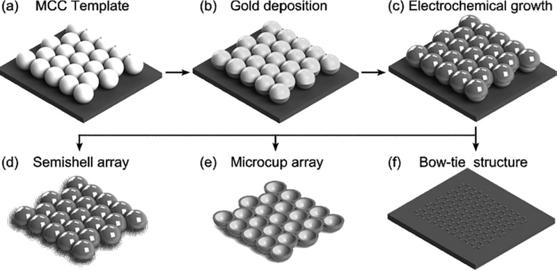
Schematic demonstration of the 3D surface pattern synthesis using template-defined site-specific electrochemical deposition. a) the MCC template; b) evaporation of gold fi lm onto the MCC template; c) template-defined site-specific electrochemical growth; d) creation of semishell array by dissolving PSs; e) microcup array generated after inversion, transfer, and removing PSs; f) bow-tie antenna structure formed on the substrate.
Figure 2.
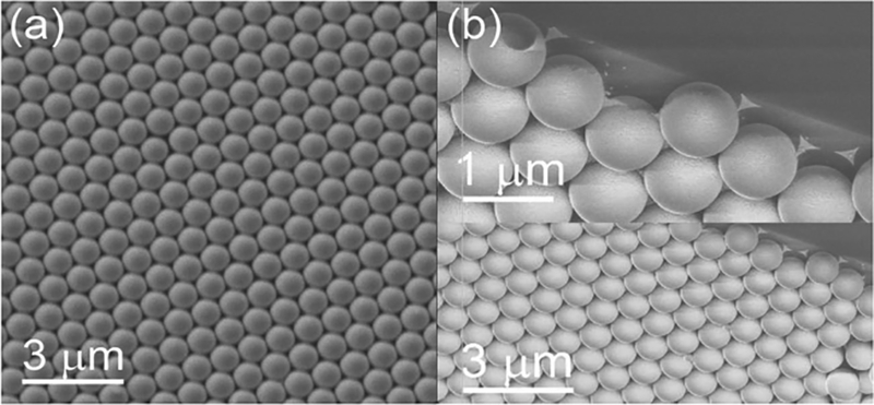
SEM image of the MCC template (a) before and (b) after gold thermal evaporation. Inset in (b) shows that the gold membrane is only deposited on the top surfaces of the PSs.
In addition, the Janus particle array can be peeled off and become freestanding on a water surface and subsequently transferred onto another substrate. This transfer also allows one to choose the orientation of the Janus particles. For instance, the Janus particles can be inverted during the transfer so that the silver surface of the particles is in contact with the substrate. This inversion process produces a microcup array after dissolution of the PSs (Figure 1e). As previously mentioned, during the thermal deposition of gold, some gold passed through the interstices between particles, creating a bow-tie structure on the substrate. Electrochemical growth of materials can be confined on the bow-tie–structured gold film and generate either the bow-tie antenna (Figure 1f) or nest-like Ag surface patterns, depending on the deposition time.
As previously mentioned, the electrochemical deposition can only emerge on the gold film, thus if the shape and/or position of the gold layer on the PS varies, Janus particles and mushroom-like clusters can be obtained. This is quite different from the situation when a bare MCC template (without the gold layer) is used during the electrochemical deposition process, where nucleation will emerge solely on the conductive substrate and materials will be deposited in the interstices between three adjacent PSs. After removing the PSs, macroporous film is obtained instead of 3D surface patterns.
2.2. Fabrication of PS-Ag Janus Particle Arrays
After electrochemical deposition using an MCC template of 1 μm PSs with the top surface covered by a layer of gold film (Figure 1, Process II), we achieved electrochemical growth of Ag on the MCC template. A lowmagnification scanning electron microscope (SEM) image exhibited that a large-area ordered array was produced (Figure 3a). Our results were verified by the XRD spectrum, showing face-centered, cubic-structured Ag (Figure S1 in the Supporting Information). The Ag deposition process did not influence the regularity of the MCC template (Figure 3b,c), but only caused the surface of the PS to become rough (Figure 3d). We observed that Ag species were only deposited on the top surface of the PS, resulting in the formation of PS-Ag Janus particle arrays, which was confirmed by Figure 3e,f. The roughness difference between the top and the bottom surfaces of the PSs could be clearly seen in Figure 3f.
Figure 3.
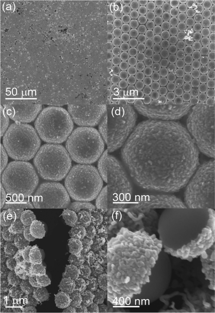
a–d) SEM images of the PS-Ag Janus particle arrays with different magnifications. e,f) Observations at the cracked areas, revealing the structure of PS-Ag Janus particles.
We analyzed the PS-Ag Janus particle array by observing the contact angle of the water-air-surface interface (Figure S2, Supporting Information). The PS-Ag Janus particle array exhibited superhydrophobic properties (contact angle: ≈150°) without any further chemical modifications. When we slowly immersed the PS-Ag Janus particle array into pure deionized water with a slanted angle (≈15°), the PS-Ag Janus particle array detached from the substrate and floated on the water surface. The freestanding PS-Ag Janus particle array was able to be transferred onto other arbitrary substrates (Figure S3, Supporting Information); in this respect, it is of particular interest to transfer the free-standing PS-Ag Janus particle array onto insulating substrates (e.g., a glass slide or plastic plate) that cannot be used for the electrochemical deposition process. This leads to many exciting opportunities such as the creation to 3D metamaterials through layer-by-layer deposition of PS-Ag Janus particles.
2.3. Fabrication of Ag 3D Semishells and Ag Bow-Tie Structures
Large-area, uniformly structured surface patterns composed of Ag 3D semishells were acquired after dissolving the PSs in toluene (Figure 4a). These Ag semishells possessed a compact hexagonal arrangement (Figure 4b,c), similar to the PSs in the preliminary MCC template. The fine structure of the Ag semishells could be clearly seen at the edge area (Figure 4d). Figure S2 (Supporting Information) shows that the Ag semi-shell 3D surface patterns can be transferred from a silicon substrate to a glass slide and that during the transferring process, the compact hexagonal structure of the Ag semishell 3D surface patterns was well-maintained.
Figure 4.
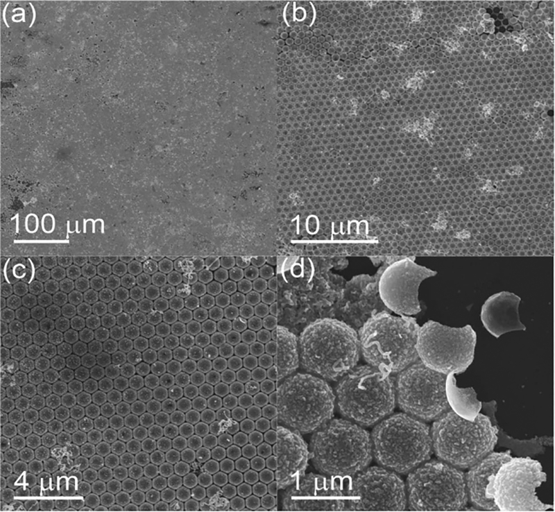
a–c) SEM images of Ag semishell 3D surface patterns with different magnifications. d) Morphology at the edge area.
After peeling off the Ag semishells from the Si substrate (using an adhesive tape), Ag bow-tie structures appeared over a large area (Figure 5), indicating that electrochemical growth of Ag on the honeycomb array of the evaporated gold nano-triangles (bottom inset in Figure 5a) also took place. The enlarged image in Figure 5b indicates that the spacing between neighboring Ag triangles is <10 nm, which is quite similar to the well-known bow-tie antenna structures.
Figure 5.
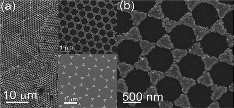
a,b) SEM images of Ag bow-tie antenna structures. Top inset in (a) is a zoom-in image. Bottom inset in (a) is the Au triangular nanoparticle array formed during the thermal evaporation process with a MCC template as a mask.
2.4. Fabrication of Inverted PS-Ag Janus Particles, Ag Microcups, and PS-Ag Mushroom-Like Clusters
Similar to the transfer process discussed for Ag semishells, the PS-Ag Janus particle array could be first inverted and then transferred onto another substrate. Highly ordered PS-Ag Janus particle arrays with the bare PS surface facing upward are shown in Figure S4a (Supporting Information). The structural uniformity was almost undisturbed during the inversion and transfer process (Figure S4b,c, Supporting Information). In the enlarged image, the bottom Ag semishells were clearly observable (Figure S4d, Supporting Information). A large-area surface pattern of Ag microcups was generated after dissolving the PS spheres in toluene (Figure 6a,b). The edge of the Ag microcup was not smooth (Figure 6c).
Figure 6.
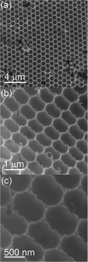
a) SEM image of Ag microcup array. b,c) Tilt-view images.
Interesting structures were created when the individual spheres in the Janus particle arrays were allowed to rotate freely. We intentionally heated the MCC template at a relative lower temperature (i.e., 100 °C) instead of the commonly used 110 °C (see the Experimental Section), leading to a weak adhesion force between the MCC template and the Si substrate. Hence, when the MCC template (with evaporated gold film) was immersed into the electrolyte solution, a significant amount of the gold-coated PSs rotated by some angle. In the subsequent electrochemical deposition process, Ag preferentially deposited on the area covered by the gold film, giving rise to mushroom-like PS-Ag heterogeneous structures with different orientations (Figure 7a,b), three and four PS-Ag mushroom-like clusters (Figure 7c,d), and multiple PS-Ag conglom erations with different orientations (10 units in Figure 7e and 13 units in Figure 7f).
Figure 7.
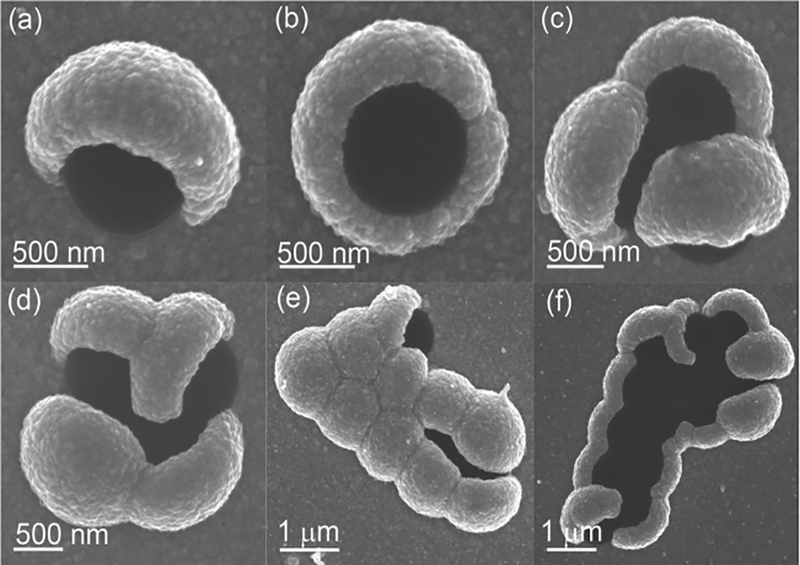
a,b) SEM images of PS-Ag Janus particles with different orientations. c,d) Three and four PS-Ag mushroom-like clusters. e,f) Multiple PS-Ag heterostructure aggregates.
2.5. Versatility of the 3D Surface Pattern Fabrication Method
As shown in previous sections, Ag will only electrochemically grow on the PS surface area that is covered by the gold layer (as opposed to a bare PS surface), supplying a powerful and reliable method to manipulate the nucleation sites during the electrochemical deposition process through control of the shape, size, and location of the gold film on the MCC template. This characteristic strengthens the structure-controlling capability of our fabrication method and increases flexibility during the on-demand design of 3D surface patterns.
We can fabricate Janus particle arrays, Ag semishells, Ag microcups, and other structures with different sizes by using different-sized PSs to form the MCC templates. For example, the size of the Ag semishells can be adjusted from less than 200 nm to more than 10 μm, depending on the size of the PSs used (200-nm to 10-μm-sized PSs are commercially available). Such versatility and flexibility renders our method valuable for many applications where the size of the structure is critical.
2.6. Fabrication of Pt and Cu 3D Surface Patterns
The versatility of our 3D surface pattern fabrication strategy lies in its ability to fabricate structures with different sizes, shapes, and compositions. In this regard, we fabricated platinum (Pt) semishell arrays. Figure 8 shows the result of a 2 min electro-chemically deposited Pt semishell surface pattern. The spectrum from energy dispersive X-ray (EDX) spectroscopy revealed that these semishells were pure Pt (Figure 8b), without the signal from the gold layer. This was due to the fact that gold film was etched away by Pt3+ ions. Magnified images showed that the surface of the Pt semishell was very rough (Figure 8c) and was formed by many Pt nanoplates (Figure 8d). Each Pt shell covered about 50% of the surface of each PS (Figure 8d).
Figure 8.
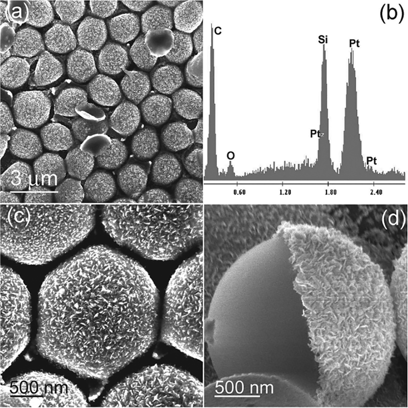
a) SEM image of 2 min deposited Pt semishell formed surface pattern. b) EDX spectrum. c) Magnified image. d) A PS-Pt Janus particle.
The fine structure of the Pt semishells could be tailored by the deposition time. When the deposition time was prolonged to 6 min, the Pt semishells were more robust and transformed into “sea urchin”-like structures (Figure 9). Many needle-like structures give the Pt semishells a high surface-area–to–volume ratio (Figure 9d). These Pt semishell arrays could be used as catalysts because of their large surface-area–to–volume ratios and the existence of a significant amount of high-index crystal planes.[50] Also, this kind of Pt semishell catalyst can be repeatedly used since these Pt semishells were anchored on a substrate. Moreover, copper (Cu) semishells were also acquired with this selective electrochemical growth method (Figure S5, Supporting Information).
Figure 9.
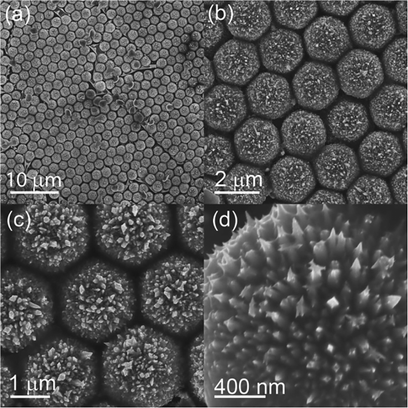
Pt semishell array fabricated with 6 min deposition. a–d) SEM images with different magnifi cations. Note the inverted Pt semishells in the center area of (a).
2.7. Fabrication of Metal Oxide 3D Surface Patterns
In addition to metal nanostructures, metal oxide nanostructures are also widely used in many areas.[51,52] The structure and morphology of metal oxide nanostructures will undoubtedly affect their properties and performances when they are used in various devices. Thus, the versatile control inherent in our template-defined electrochemical growth technique is ideal for the fabrication of metal oxide 3D surface patterns. Among various metal oxides, MnO2 is an important and widely studied electrode material in supercapacitors and lithium-ion batteries.[51,52] Therefore, we take MnO2 as a model material to study the feasibility of the selective electrochemical growth technique in creating metal oxide 3D surface patterns. MnO2 semishell arrays were successfully generated on the anode electrode (Figure 10a,b). The hollow structure of the semishell shown in the inset of Figure 10a gives the structure a high surface-area–to–volume ratio. The surface-area-to-volume ratio is further intensified by a rough surface formed from a tremendous amount of small nanoplates (Figure 10c).
Figure 10.
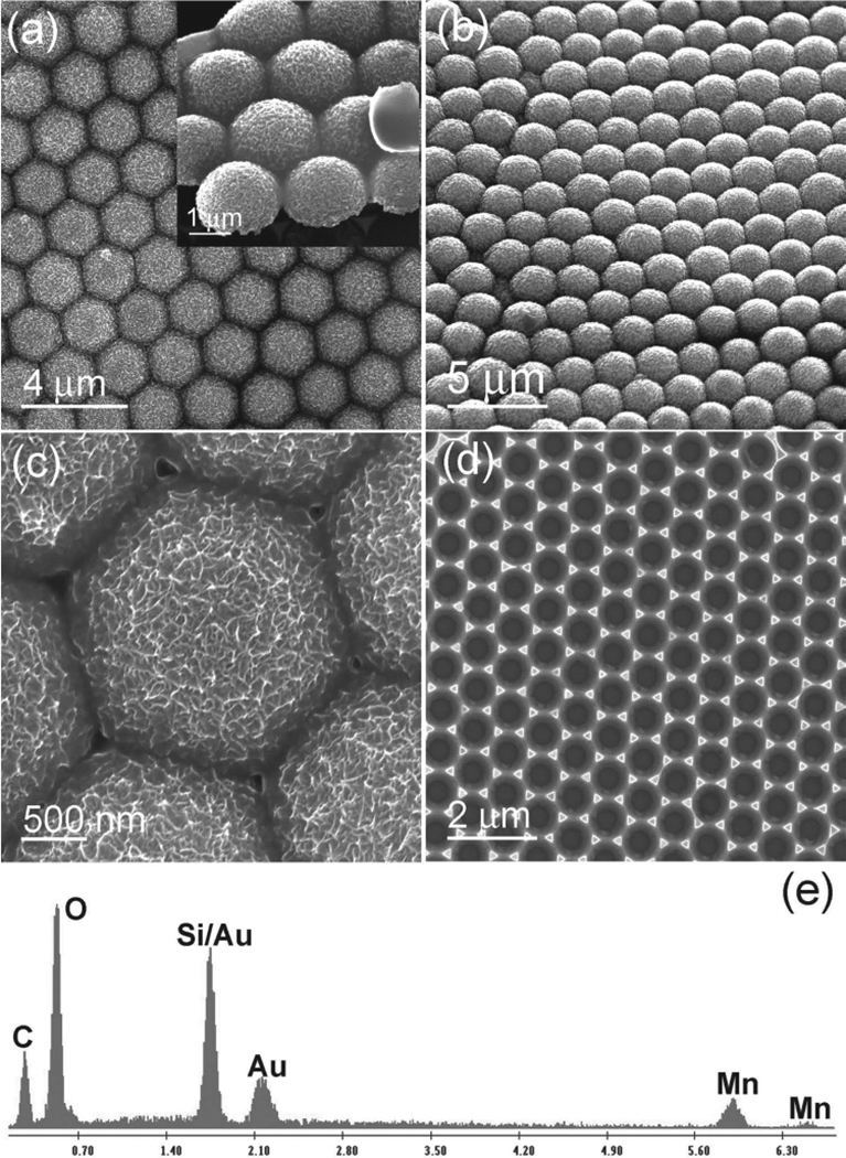
a) SEM image of MnO2 semishell surface patterns. Inset in is the tilt-view image. c) Enlarged image. d) Fishnet-like MnO2 porous structures after removing the top MnO2 semishell layer. e) EDX spectrum.
The EDX spectrum of these semishell surface patterns (Figure 10e) indicates that the element ratio between Mn and O was about 1:2, implying that these semishells were MnO2. It is important to note that the gold layer was still lying below the MnO2 semishells, as verified by the EDX spectrum. The existence of the gold layer resolves the detrimentally poor conductivity bottleneck of MnO2 when it is used as an electrode in supercapacitors.[51,52] Single-layered MnO2 semishell arrays might be used in compact supercapacitors. Good performance is anticipated if these MnO2 semishell arrays are applied as electrodes in supercapacitors. After removing the MnO2 semishells by a piece of adhesive tape, honeycomb-like MnO2 porous membranes emerged on the Si substrate (Figure 10d). Thus, after the selective electrochemical growth of the gold-coated PS array on the Si substrate, two layers of MnO2 formed simultaneously, with the top layer being the semishell array, and the bottom layer being the honeycomb-like structure on the Si substrate (see Figure 1). These two layers of MnO2, prepared in one step, could be used as anode and cathode electrodes for lithium-ion batteries, resulting in micrometer-thick, extremely compact energy storage devices.
2.8. Fabrication of Conductive Polymer 3D Surface Patterns
Our fabrication strategy can be conveniently extended into the preparation of 3D surface patterns of conductive polymers. Polyaniline (PANI) nanostructures have been widely studied in various applications, such as sensing, photovoltaic cells, supercapacitors, nano-actuators, and artificial muscles.[53–57] We demonstrate that semishell arrays of PANI were successfully prepared through selective electro-polymerization of aniline on the MCC template covered by a gold layer (Figure S6, Supporting Information). 3D surface patterns of other conductive polymers (e.g., poly(pyrrole)s, poly(thiophene-3-acetic acid)) can also be fabricated using our approach.
2.9. SERS Sensing of the Prepared Ag 3D Surface Patterns
The 3D surface patterns described in previous sections have a wide range of potential applications. As an example, we investigated the surface-enhanced Raman scattering (SERS)[58–62] sensing performance of the fabricated Ag 3D semishell arrays. Using rhodamine 6G (R6G) as a probing molecule, we found that the Ag semishells showed even stronger SERS enhancement (curve a in Figure 11) than the well-known bow-tie–structured Ag (curve b in Figure 11) under the excitation wavelength of 532 nm. The stronger SERS enhancement is caused by the 3D structure of the semishells. A large amount of “hot spots” are integrated in both the rough semishells themselves and within the nanometer-scale crevices between neighboring semishells in the 3D surface patterns. Furthermore, the laser light is more efficiently used to generate the SERS signal during the Raman spectrum detection induced by the 3D structure of the semishells (i.e., 3D structure-induced SERS enhancement). The enhancement factor of these Ag semishells is estimated to be on the order of 107 (under the excitation wavelength of 532 nm) based on previously reported calculation methods.[9] Ag microcups (see Figure 5) with the openings oriented upward should also show strong SERS sensitivity, owing to the sharp edges of these microcups together with their rough surfaces. However, as shown in Figure 11 (curve c), the SERS signal from the Ag microcup arrays was very weak. This is partly due to the fact that the inner surface of the Ag microcups is essentially the evaporated thin gold film, which usually shows weaker SERS sensitivity compared with Ag nanostructures. This hypothesis was confirmed in our control experiment: at the same detection parameters and the same R6G concentrations (10−8 M), gold film (about 10 nm thick) evaporated on a glass slide showed no signals (curve d in Figure 11).
Figure 11.
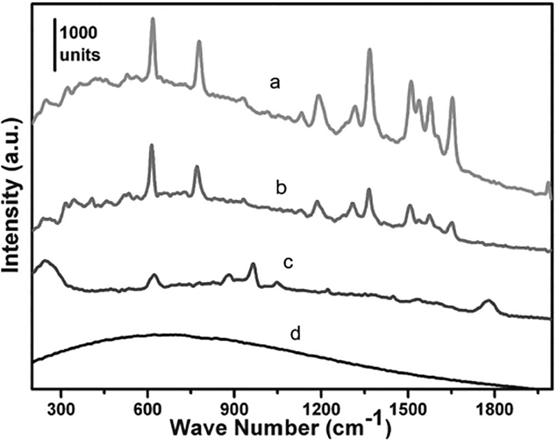
Raman spectra of R6G molecules absorbed on Ag semishell 3D surface patterns (curve a), bow-tie-antenna-structured Ag (curve b), microcup arrays (curve c, 20× enlargement), and gold thin-film on a glass slide (curve d) under 532 nm laser excitation.
In order to thoroughly understand the SERS performance of the synthesized 3D Ag surface patterns, finite-difference time-domain (FDTD) simulations were carried out to simulate the local electromagnetic field distributions within the Ag 3D surface patterns. As shown in Figure 12a, there were only two areas within the microcups that have strong local electric field enhancement, and these areas are not close to the surface. Since the probing molecules were closely located (several nanometers apart) at the inner surface of the microcups, the effective local electric field amplitude contributing to the SERS enhancement is quite weak, leading to poor SERS enhancement performance from Ag microcup arrays. In contrast, the local electric field amplitude near (<5 nm) the whole Ag semishell surface was extremely high, as shown in Figure 12b. Therefore, the 3D-structured semishells are very beneficial for enhancing the Raman signal from the molecules tightly attached on their surfaces. In the FDTD simulations, we used Ag semishells with smooth surfaces as a model for simplicity, and if the rough surface of the Ag semishell is taken into account, the local electric field should be even stronger. It should be noted that the SERS enhancement factor is highly dependent to the excitation wavelength (532 nm laser was used here) and the influence of the excitation wavelength on the SERS enhancement factor from different Ag surface patterns will be studied in the future.
Figure 12.
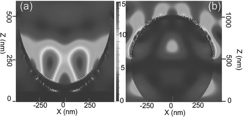
Electromagnetic field amplitude patterns from FDTD calculations at the excitation wavelength of 532 nm for (a) Ag microcup and (b) Ag semishell.
3. Conclusion
We have demonstrated the large-scale fabrication of 3D surface patterns using a selective electrochemical growing process on MCC templates. Our method can produce 3D surface patterns with different structures (including semishells, Janus particles, microcups, and mushroom-like clusters). More importantly, it can be used to synthesize well-defined 3D surface patterns with prescribed compositions (metals, metal oxides, metal sulfides, or conductive polymers). In a proof-of-concept study, we demonstrate that 3D Ag semishell arrays fabricated by our approach exhibit excellent SERS properties under 532 nm laser excitation. The 3D surface pattern fabrication technique presented here is versatile, convenient, rapid, inexpensive, and reliable. With these advantages, it opens up a new avenue toward designing and synthesizing 3D surface patterns for various applications.
4. Experimental Section
4.1. MCC Template Synthesis and Gold Thermal Evaporation
Monolayer colloidal crystal (MCC) templates formed by PSs were prepared by a spin-coating method as previously reported.[9,20,46,47] The as-prepared MCC templates were heated at 110 °C for 10 min in order to reinforce the adhesion between the PS spheres and the Si substrates beneath (if the heating temperature is lower, PSs could rotate or be detached during the immersion into the electrolyte solution). Consequently, a layer of gold film was thermally evaporated on the MCC template surface using a thermal evaporator. Thermal evaporation was carried out at 10−6 mbar and the evaporation speed was maintained at 0.02 nm per second. The thickness of the gold film was about 10 nm. Due to the shadow effects, gold will only be deposited on the top surfaces of the PSs. MCC templates with the evaporated gold membranes were used directly as electrodes to conduct subsequent electrochemical deposition of various materials.
4.2. Electrochemical Deposition
Electrochemical deposition was carried out under a potentio-static mode within a two-electrode cell. The counter electrode was a cleaned Si wafer with resistivity of about 0.02 Ω cm. The electrolyte solution for electrochemical deposition of Ag was prepared by dissolving 0.1 g sodium dodecyl sulphate and 0.5 g AgNO3 into 40 mL deionized water. The deposition voltage was 10 V. For Pt deposition, the electrolyte was made by dissolving 0.1 g H2PtCl6 into 40 mL deionized water. 4 V was used as the deposition voltage. For Cu deposition, 0.5 g CuSO4 · 5H2O was added to 40 mL deionized water (a small amount of CuOx (0 < x < 2) was involved) under a voltage of 5 V. For the deposition of Ag, Pt, and Cu, the MCC template was used as the cathode electrode. For the electrochemical deposition of MnO2 and PANI, the MCC template was used as the anode electrode. For the deposition of MnO2, 40 mL (0.01 M) Mn(Ac)2 was used as the electrolyte, and the deposition voltage was 5 V. For the deposition of PANI, 450 μL aniline was dissolved into 100 mL deionized water together with 0.4 mL HCl (1M) to form the electrolyte, and the deposition voltage was 5 V. The electrochemical deposition time for Ag, Cu, and PANI was 30 min. The deposition time for Pt was varied from 2 to 6 min in order to study the influence of deposition time on the structure of the prepared Pt 3D surface patterns. The MnO2 deposition time was 6 min. After the electrochemical deposition growth of Ag, PSs in the MCC template with the top surfaces enclosed by a layer of Ag were acquired. Microcup arrays of Ag, Pt, Cu, PANI, and MnO2 were acquired by dissolving PSs with toluene or CH2Cl2.
4.3. SERS Measurement
Ag 3D surface patterns were incubated in 10−8 M rhodamine 6G (R6G) aqueous solutions (with a small amount of ethanol) for 1 h and then rinsed with deionized water before Raman spectral detections. The Raman scattering spectra were recorded with a confocal microprobe Raman system with the excitation wavelength of 532 nm. The accumulation time was maintained at 10 s. The Raman detections were repeated at five randomly chosen sites, showing small intensity deviations (less than 15%).
Supplementary Material
Acknowledgements
We gratefully acknowledge the financial support from National Institutes of Health (Director’s New Innovator Award, 1DP2OD007209–01), National Science Foundation, the Penn State Center for Nanoscale Science (MRSEC), European Research Council (ERC) Grant (3D Surface), and Federal Ministry of Education and Research (BMBF, ZIK II). B.C. Cao also thanks the Taishan Scholar Professorship (TSHW20091007), the Program for New Century Excellent Talents in University (NCET-11–1027), Ministry of Education, China, and the Shandong Provincial Science Foundation for Disguised Youth Scholars (2012JQB01031; BS2010CL003). Components of this work were conducted at the Penn State node of the NSF-funded National Nanotechnology Infrastructure Network.
Footnotes
Supporting Information
Supporting Information is available from the Wiley Online Library or from the author.
Contributor Information
Shikuan Yang, Department of Engineering Science and Mechanics, The Pennsylvania State University, University Park, PA 16802-6812, USA.
Michael Ian Lapsley, Department of Engineering Science and Mechanics, The Pennsylvania State University, University Park, PA 16802-6812, USA.
Bingqiang Cao, School of Materials Science and Engineering, University of Jinan, Jinan 250022, China.
Chenglong Zhao, Department of Engineering Science and Mechanics, The Pennsylvania State University, University Park, PA 16802-6812, USA.
Yanhui Zhao, Department of Engineering Science and Mechanics, The Pennsylvania State University, University Park, PA 16802-6812, USA.
Qingzhen Hao, Department of Engineering Science and Mechanics, The Pennsylvania State University, University Park, PA 16802-6812, USA.
Brian Kiraly, Department of Engineering Science and Mechanics, The Pennsylvania State University, University Park, PA 16802-6812, USA.
Jason Scott, Department of Engineering Science and Mechanics, The Pennsylvania State University, University Park, PA 16802-6812, USA.
Weizhou Li, School of Materials Science and Engineering, Guangxi University, Nanning 530004, China.
Lin Wang, Ascent Bio-Nano Technologies Inc., State College, PA 16801, USA.
Yong Lei, Email: yong.lei@tu-ilmenau.de, Center for Innovation Competence & Institute for Physics, Technical University of Ilmenau, 98693 Ilmenau, Germany.
Tony Jun Huang, Email: junhuang@psu.edu, Department of Engineering Science and Mechanics, The Pennsylvania State University University Park, PA 16802-6812, USA.
References
- [1].Kim J, Hanna JA, Byun M, Santangelo CD, Hayward RC, Science 2012, 335, 1201. [DOI] [PubMed] [Google Scholar]
- [2].Schlapak R, Danzberger J, Armitage D, Morgan D, Ebner A, Hinterdorfer P, Pollheimer P, Gruber HJ, Schaffler F, Howorka S, Small 2012, 8, 89. [DOI] [PubMed] [Google Scholar]
- [3].a) Menezes JW, Ferreira J, Santos MJL, Cescato L, Brolo AG, Adv. Funct. Mater 2010, 20, 3918; [Google Scholar]; b) Hsiao VKS, Waldeisen JR, Zheng Y, Lloyd PF, Bunning TJ, Huang TJ, J. Mater. Chem 2007, 17, 4896; [Google Scholar]; c) Huang TJ, Liu M, Knight LD, Grody WW, Miller JF, Ho C-M, Nucleic Acids Res. 2012, 30, e55. [DOI] [PMC free article] [PubMed] [Google Scholar]
- [4].Caironi M, Gili E, Sakanoue T, Cheng XY, Sirringhaus H, ACS Nano 2010, 4, 1451. [DOI] [PubMed] [Google Scholar]
- [5].Khang DY, Jiang HQ, Huang Y, Rogers JA, Science 2006, 311, 5758. [DOI] [PubMed] [Google Scholar]
- [6].a) Medina-Sánchez M, Miserere S, Merkoçi A, Lab Chip 2012, 12, 1932; [DOI] [PubMed] [Google Scholar]; b) Shi J, Mao X, Ahmed D, Colletti A, Huang TJ, Lab Chip 2008, 8, 221; [DOI] [PubMed] [Google Scholar]; c) Shi J, Ahmed D, Mao X, Lin S-CS, Huang TJ, Lab Chip 2009, 9, 2890; [DOI] [PubMed] [Google Scholar]; d) Shi J, Yazdi S, Lin S-CS, Ding X, Chiang I-K, Sharp K, Huang TJ, Lab Chip 2011, 11, 2319; [DOI] [PMC free article] [PubMed] [Google Scholar]; e) Mao X, Huang TJ, Lab Chip 2012, 12, 1412; [DOI] [PMC free article] [PubMed] [Google Scholar]; f) Ding X, Lin S-CS, Kiraly B, Yue H, Li S, Shi J, Benkovic SJ, Huang TJ, Proc. Natl. Acad. Sci. USA 2012, 109, 11105. [DOI] [PMC free article] [PubMed] [Google Scholar]
- [7].Cavallini M, Biscarini F, Leon S, Zerbetto F, Bottari G, Leigh DA, Science 2003, 299, 531. [DOI] [PubMed] [Google Scholar]
- [8].Wan D, Chen H, Tseng S, Wang L, Chen Y, ACS Nano 2010, 4, 165. [DOI] [PubMed] [Google Scholar]
- [9].Yang SK, Xu F, Ostendorp S, Wilde G, Zhao H, Lei Y, Adv. Funct. Mater 2011, 21, 2446. [Google Scholar]
- [10].a) Zheng YB, Jensen L, Yan W, Walker TR, Juluri BK, Jensen L, Huang TJ, Nano Lett. 2009, 9, 819; [DOI] [PubMed] [Google Scholar]; b) Hsiao VKS, Zheng YB, Juluri BK, Huang TJ, Adv. Mater 2008, 20, 3528. [Google Scholar]
- [11].Aksu S, Huang M, Artar A, Yanik AA, Selvarasah S, Dokmeci MR, Altug H, Adv. Mater 2011, 23, 4422. [DOI] [PubMed] [Google Scholar]
- [12].Nagpal P, Lindquist NC, Oh SH, Norris DJ, Science 2009, 325, 594. [DOI] [PubMed] [Google Scholar]
- [13].Zhou W, Gao H, Odom TW, ACS Nano 2010, 4, 1241. [DOI] [PubMed] [Google Scholar]
- [14].a) Liu N, Hentschel M, Weiss T, Alivisatos AP, Giessen H, Science 2011, 332, 1407; [DOI] [PubMed] [Google Scholar]; b) Liu N, Mesch M, Weiss T, Hentschel M, Giessen H, Nano Lett. 2010, 10, 2342; [DOI] [PubMed] [Google Scholar]; c) Liu YJ, Zheng YB, Shi J, Huang H, Walker TR, Huang TJ, Opt. Lett 2009, 34, 2351. [DOI] [PubMed] [Google Scholar]
- [15].a) Halas NJ, Lal S, Chang WS, Link S, Nordlander P, Chem. Rev 2011, 111, 3913; [DOI] [PubMed] [Google Scholar]; b) Juluri BK, Zheng YB, Ahmed D, Jensen L, Huang TJ, J. Phys. Chem. C 2008, 112, 7309; [Google Scholar]; c) Liu YJ, Hao Q, Smalley JST, Liou J, Khoo IC, Huang TJ, Appl. Phys. Lett 2010, 97, 091101; [Google Scholar]; d) Li D, Baughman RH, Huang TJ, Stoddart JF, Weiss PS, MRS Bull. 2009, 34, 671; [Google Scholar]; e) Le F, Brandl DW, Urzhumov YA, Wang H, Kundu J, Halas NJ, Aizpurua J, Nordlander P, ACS Nano 2008, 2, 707. [DOI] [PubMed] [Google Scholar]
- [16].a) Fan JA, Wu CH, Bao K, Bao JM, Bardhan R, Halas NJ, Manoharan VN, Nordlander P, Shvets G, Capasso F, Science 2010, 328, 1135; [DOI] [PubMed] [Google Scholar]; b) Fan JA, Bao K, Wu CH, Bao JM, Bardhan R, Halas NJ, Manoharan VN, Shvets G, Nordlander P, Capasso F Nano Lett. 2010, 10, 4680. [DOI] [PubMed] [Google Scholar]
- [17].a) Rycenga M, Cobley CM, Zeng J, Li WY, Moran CH, Zhang Q, Qin D, Xia YN, Chem. Rev 2011, 111, 3669; [DOI] [PMC free article] [PubMed] [Google Scholar]; b) Xia YN, Xiong YJ, Lim B, Skrabalak SE, Angew. Chem. Int. Ed 2009, 48, 60. [DOI] [PMC free article] [PubMed] [Google Scholar]
- [18].Tian C, Ding C, Liu S, Yang S, Song X, Ding B, Li Z, Fang J, ACS Nano 2011, 5, 9442. [DOI] [PubMed] [Google Scholar]
- [19].Zeng H, Xu X, Bando Y, Gautam UK, Zhai T, Fang X, Liu B, Golberg D, Adv. Funct. Mater 2009, 19, 3165. [Google Scholar]
- [20].Lei Y, Yang SK, Wu MH, Wilde G, Chem. Soc. Rev 2011, 40, 1247. [DOI] [PubMed] [Google Scholar]
- [21].Ye X, Qi L, Nano Today 2011, 6, 608. [Google Scholar]
- [22].Choi M, Lee SH, Kim Y, Kang SB, Shin J, Kwak MH, Kang KY, Lee YH, Park N, Min B, Nature 2011, 470, 369. [DOI] [PubMed] [Google Scholar]
- [23].Giselbrecht S, Reinhardt M, Mappes T, Borner M, Gottwald E, van Blitterswijk C, Saile V, Truckenmuller R, Adv. Mater 2011, 23, 4873. [DOI] [PubMed] [Google Scholar]
- [24].Christman KL, Schopf E, Broyer RM, Li RC, Chen Y, Maynard HD, J. Am. Chem. Soc 2008, 131, 521. [DOI] [PMC free article] [PubMed] [Google Scholar]
- [25].Dubey M, Emoto K, Takahashi H, Castner DG, Grainger DW, Adv. Funct. Mater 2009, 19, 3046. [DOI] [PMC free article] [PubMed] [Google Scholar]
- [26].Coyer SR, Garcia AJ, Delamarche E, Angew. Chem. Int. Ed 2007, 46, 6837. [DOI] [PubMed] [Google Scholar]
- [27].Kostovski G, Chinnasamy U, Jayawardhana S, Stoddart PR, Mitchell A, Adv. Mater 2011, 23, 531. [DOI] [PubMed] [Google Scholar]
- [28].Slater JH, Miller JS, Yu SS, West JL, Adv. Funct. Mater 2011, 21, 2876. [DOI] [PMC free article] [PubMed] [Google Scholar]
- [29].Garcia A, Polesel-Maris J, Viel P, Palacin S, Berthelot T, Adv. Funct. Mater 2011, 21, 2096. [Google Scholar]
- [30].Baek Y-K, Yoo SM, Kang T, Jeon H-J, Kim K, Lee J-S, Lee SY, Kim B, Jung H-T, Adv. Funct. Mater 2010, 20, 4273. [Google Scholar]
- [31].Ofir Y, Samanta B, Xiao Q, Jordan BJ, Xu H, Arumugam P, Arvizo R, Tuominen MT, Rotello VM, Adv. Mater 2008, 20, 2561. [Google Scholar]
- [32].Maaroof AL, Cortie MB, Harris N, Wieczorek L, Small 2008, 4, 2292. [DOI] [PubMed] [Google Scholar]
- [33].King NS, Li Y, Ayala-Orozco C, Brannan T, Nordlander P, Halas NJ, ACS Nano 2011, 5, 7254. [DOI] [PubMed] [Google Scholar]
- [34].Mirin NA, Halas NJ, Nano Lett. 2009, 9, 1255. [DOI] [PubMed] [Google Scholar]
- [35].Zhang Y, Barhoumi A, Lassiter JB, Halas NJ, Nano Lett. 2011, 11, 1838. [DOI] [PubMed] [Google Scholar]
- [36].Dorpe PV, Ye J, ACS Nano 2011, 5, 6774. [DOI] [PubMed] [Google Scholar]
- [37].Hulteen JC, Van Duyne RP, J. Vac. Sci. Technol., A 1995, 13, 1553. [Google Scholar]
- [38].a) Yang SK, Lei Y, Nanoscale 2011, 3, 2768; [DOI] [PubMed] [Google Scholar]; b) Li Y, Koshizaki N, Cai WP, Coord. Chem. Rev 2011, 255, 357; [Google Scholar]; c) Li Y, Cai WP, Duan GT, Chem. Mater 2008, 20, 615. [Google Scholar]
- [39].Zhang J, Li Y, Zhang X, Yang B, Adv. Mater 2010, 22, 4249; [DOI] [PubMed] [Google Scholar]; Zhang J, Yang B, Adv. Funct. Mater 2010, 20, 3411. [DOI] [PMC free article] [PubMed] [Google Scholar]
- [40].Hong G, Li C, Qi L, Adv. Funct. Mater 2010, 20, 3774. [Google Scholar]
- [41].Polyushkin DK, Hendry E, Stone EK, Barnes WL, Nano Lett. 2011, 11, 4718. [DOI] [PubMed] [Google Scholar]
- [42].Vogel N, Fischer J, Mohammadi R, Retsch M, Butt H, Land-fester K, Weiss CK, Kreiter M, Nano Lett. 2011, 11, 446. [DOI] [PubMed] [Google Scholar]
- [43].Vogel N, Jung M, Bocchio NL, Retsch M, Kreiter M, Koper I, Small 2010, 6, 104. [DOI] [PubMed] [Google Scholar]
- [44].Gwinner MC, Koroknay E, Fu LW, Patoka P, Kandulski W, Giersig M, Giessen H, Small 2009, 5, 400. [DOI] [PubMed] [Google Scholar]
- [45].Kosiorek A, Kandulski W, Glaczynska H, Giersig M, Small 2005, 1, 439. [DOI] [PubMed] [Google Scholar]
- [46].a) Li Y, Fang XS, Koshizaki N, Sasaki T, Li L, Gao SY, Shimizu Y, Bando Y, Golberg D, Adv. Funct. Mater 2009, 19, 2467; [Google Scholar]; b) Li Y, Sasaki T, Shimizu Y, Koshizaki N, Small 2008, 4, 2286; [DOI] [PubMed] [Google Scholar]; c) Li Y, Sasaki T, Shimizu Y, Koshizaki N, J. Am. Chem. Soc 2008, 130, 14755. [DOI] [PubMed] [Google Scholar]
- [47].a) Yang SK, Cai WP, Yang JL, Zeng HB, Langmuir 2009, 25, 8287; [DOI] [PubMed] [Google Scholar]; b) Yang SK, Cai WP, Kong LC, Lei Y, Adv. Funct. Mater 2010, 20, 2527. [Google Scholar]
- [48].Duan GT, Cai WP, Luo YY, Sun FQ, Adv. Funct. Mater 2007, 17, 644. [Google Scholar]
- [49].a) Retsch M, Tamm M, Boccio N, Horn N, Forch R, Kreiter USM, Small 2009, 5, 2105; [DOI] [PubMed] [Google Scholar]; b) Li C, Hong GS, Qi LM, Chem. Mater 2010, 22, 476; [Google Scholar]; c) Li C, Hong GS, Wang PW, Yu DP, Qi LM, Chem. Mater 2009, 21, 891; [Google Scholar]; d) Huang T, Zhao QA, Xiao JY, Qi LM, ACS Nano 2010, 4, 4707. [DOI] [PubMed] [Google Scholar]
- [50].Tian N, Zhou Z, Sun S, Ding Y, Wang Z, Science 2007, 316, 732. [DOI] [PubMed] [Google Scholar]
- [51].Reddy ALM, Shaijumon MM, Gowda SR, Ajayan PM, Nano Lett. 2009, 9, 1002. [DOI] [PubMed] [Google Scholar]
- [52].Liu JP, Jiang J, Cheng CW, Li HX, Zhang JX, Gong H, Fan HJ, Adv. Mater 2011, 23, 2076. [DOI] [PubMed] [Google Scholar]
- [53].Wang YG, Li HQ, Xia YY, Adv. Mater 2006, 18, 2619. [Google Scholar]
- [54].Ding MN, Tang YF, Gou PP, Reber MJ, Star A, Adv. Mater 2011, 23, 536. [DOI] [PubMed] [Google Scholar]
- [55].Spinks GM, Mottaghitalab V, Bahrami-Saniani M, Whitten PG, Wallace GG, Adv. Mater 2006, 18, 637. [Google Scholar]
- [56].Zou W, Wang W, He B, Sun M, Yin Y, J. Power Sources 2010, 195, 7489. [Google Scholar]
- [57].Chen L, Sun L, Luan F, Liang Y, Li Y, Liu X, J. Power Sources 2010, 195, 3742. [Google Scholar]
- [58].a) Yang SK, Cao BQ, Kong LC, Wang ZY, J. Mater. Chem 2011, 21, 14031; [Google Scholar]; b) Liang HY, Li ZP, Wang WZ, Wu YS, Xu HX, Adv. Mater 2009, 21, 4614. [Google Scholar]
- [59].a) Yan B, Thubagere A, Premasiri WR, Ziegler LD, Dal Negro L, Reinhard BM, ACS Nano 2009, 3, 1190; [DOI] [PubMed] [Google Scholar]; b) Yang LL, Yan B, Premasiri WR, Ziegler LD, Dal Negro L, Reinhard BM, Adv. Funct. Mater 2010, 20, 2619. [Google Scholar]
- [60].a) Alvarez-Puebla RA, Liz-Marzan LM, Chem. Soc. Rev 2012, 41, 43; [DOI] [PubMed] [Google Scholar]; b) Fang J, Du S, Lebedkin S, Li Z, Kruk R, Kappes M, Hahn H, Nano Lett. 2010, 10, 5006. [DOI] [PubMed] [Google Scholar]
- [61].Kneipp J, Kneipp H, Kneipp K, Chem. Soc. Rev 2008, 37, 1052. [DOI] [PubMed] [Google Scholar]
- [62].Banholzer MJ, Millstone JE, Qin LD, Mirkin CA, Chem. Soc. Rev 2008, 37, 885. [DOI] [PMC free article] [PubMed] [Google Scholar]
Associated Data
This section collects any data citations, data availability statements, or supplementary materials included in this article.


