

Strain-induced Landau levels in wafer-scale graphene at room temperature are studied using momentum-resolved spectroscopy.
Abstract
Graphene is a powerful playground for studying a plethora of quantum phenomena. One of the remarkable properties of graphene arises when it is strained in particular geometries and the electrons behave as if they were under the influence of a magnetic field. Previously, these strain-induced pseudomagnetic fields have been explored on the nano- and micrometer-scale using scanning probe and transport measurements. Heteroepitaxial strain, in contrast, is a wafer-scale engineering method. Here, we show that pseudomagnetic fields can be generated in graphene through wafer-scale epitaxial growth. Shallow triangular nanoprisms in the SiC substrate generate strain-induced uniform fields of 41 T, enabling the observation of strain-induced Landau levels at room temperature, as detected by angle-resolved photoemission spectroscopy, and confirmed by model calculations and scanning tunneling microscopy measurements. Our work demonstrates the feasibility of exploiting strain-induced quantum phases in two-dimensional Dirac materials on a wafer-scale platform, opening the field to new applications.
INTRODUCTION
Graphene, a single atomic layer of carbon atoms arranged in a honeycomb lattice, holds great promise for numerous applications due to its remarkable mechanical, optical, and electronic properties. In addition, owing to the linearly dispersing electronic bands (1–3), graphene also serves as a prototypical material platform for studying relativistic Dirac fermions. Graphene was also the first material in which a member of the marked class of macroscopic quantum phenomena (4–7), the quantum Hall effect (QHE) (8), could be observed at room temperature when subject to large magnetic fields (9). In the quantum Hall state, charge carriers are forced into cyclotron orbits with quantized radii and energies known as Landau levels (LLs), once subjected to the influence of a magnetic field. To observe this effect, certain conditions must be met: The magnetic field must be large enough that the resulting spacing between LLs is larger than the thermal energy (ΔELL > kBT), the charge carrier lifetime between scattering events must be longer than the characteristic time of the cyclotron orbit (tlife > 1/ωc), and the magnetic field must be uniform on length scales greater than the LL orbit. This typically mandates the need for cryogenic temperatures, clean materials, and large applied magnetic fields. Dirac fermions in graphene provide a way to lift these restrictions: Under certain strain patterns, graphene’s electrons behave as if they were under the influence of large magnetic fields, without applying an actual field from outside the material (10–13). These so-called pseudomagnetic fields only couple to the relativistic electrons around the Dirac point and, under the QHE conditions above, lead to the formation of flat quantized LLs. This has been successfully observed using a range of methods (11–13), but was so far restricted to small regions, which severely limits its applicability.
RESULTS
Here, we directly visualize the formation of flat LLs close to the Fermi energy induced by pseudomagnetic fields on wafer-scale semiconductor samples. By measuring the hallmark energy spacing and momentum dependence of the ensuing pseudo-LLs with angle-resolved photoemission spectroscopy (ARPES) and with the aid of model calculations, we confirm their quantum Hall nature and extract a pseudomagnetic field strength of B = 41 T. This is made possible by the presence of a distribution of triangular nanoprisms underneath the monolayer graphene in our samples based on the well-established platform of epitaxial graphene on SiC substrates (14–17), as revealed by a combination of atomic force microscopy (AFM) and scanning tunneling microscopy (STM) measurements.
Our topographic images of these samples (Fig. 1A, inset) exhibit the well-known terraces and step edges of graphene grown on 6H-SiC (14), which are due to a miscut of the wafers from the (0001) direction of up to 0. 1∘. A population of triangular-shaped nanoscale features is identified on the terraces of our samples (Fig. 1A), which appear similar to those reported on similar substrates (18, 19). These nanoprisms appear during the growth process of graphene on 6H-SiC and are controllable by the Argon flow in the chamber (19). They cover between 5 and 10% of the terraces and are completely covered by monolayer graphene, the latter being demonstrated by our AFM adhesion images (see figs. S8 and S9B). They are equilateral, have a narrow size distribution around 300-nm side length, are oriented in the same direction, and are about deep (Fig. 1B), which corresponds to a single missing SiC double layer or one-sixth of the 6H-SiC unit cell. This leads to a change in the registry between the silicon atoms in the top layer of the substrate and the graphene, as illustrated in Fig. 1D. The strain created inside the nanoprisms cannot be relieved because the nanostructures are continuously covered by monolayer graphene without additional grain boundaries, as corroborated by our STM images across the edge (see fig. S9A). To get a more detailed view of the strain pattern, we perform additional detailed atomic resolution STM measurements. The images taken inside and outside the nanoprisms (Fig. 1E) show the expected modulation with respect to SiC on top of the carbon honeycomb lattice (20). However, taking the difference of the two Fourier-transformed images (Fig. 1F) reveals a shear strain pattern inside the nanoprism, with a maximal observed strain of approximately 3∘.
Fig. 1. Identification of strained nanoprisms.
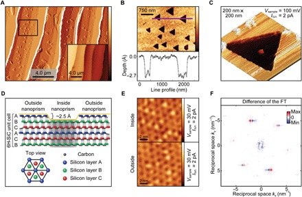
(A) Horizontal derivative AFM topography image of our monolayer graphene grown on a SiC substrate. Triangular nanoprisms are dispersed on the surface. Inset: AFM topography image of the same area. Substrate terrace steps are approximately 10 nm in height. (B) Top: Close-up view of AFM topography of the area indicated by the black box in (A). Bottom: Line cut through the AFM data marked by the purple line in the close-up view. (C) Overview STM topography image (200 nm × 200 nm, Vsample = 100 mV, Itun. = 2 pA) showing a single nanoprism. (D) Schematic structure of 6H-SiC showing its layered ABCACB stacking order with epitaxial graphene on top (yellow). Inside the nanoprism, a single layer within the unit cell is missing, exposing the graphene to a different substrate surface termination, as illustrated in the top view. The carbon buffer layer is not shown for clarity. (E) Atomically resolved STM images (10 nm × 10 nm, Vsample = 30 mV, Itun. = 2 pA) inside (top) and outside (bottom) of the nanoprism. (F) Difference map of the two Fourier transformed (FT) images in (E) visualizing the strain pattern inside the nanoprism.
To confirm whether the induced strain pattern leads to flat LLs close to the Fermi energy, we perform a series of high-resolution ARPES measurements. ARPES is a momentum- and energy-resolved technique that has proven to be a powerful tool in directly studying the electronic band structures of a vast variety of quantum phases of matter from strongly correlated electron systems and high-Tc superconductors (21) to topological insulators and semimetals (22–24). However, no study of quantum Hall states has been performed, since ARPES is strictly incompatible with the application of magnetic fields, as essential crystal momentum information carried by the photoemitted electrons would be lost through interaction with the field. This, however, is different for pseudomagnetic fields, as they only interact with the Dirac electrons inside the material. We note that, while a recently developed momentum-resolved technique amenable to magnetic fields has been reported (25), it necessarily requires sophisticated heterostructures and physically accessible fields and is limited to a small sector of the Brillouin zone.
Our ARPES data, which, due to the ∼1-mm spot size of the photon source, correspond to the spatial average over unstrained and strained regions of the sample, show the expected Dirac cone and new flat bands that gradually merge with the linear dispersion (Fig. 2, A and C). The unequal energy spacing of these newly observed bands can be extracted from cuts along the energy direction at the K point (Fig. 2B) and their second derivative (Fig. 2D). By plotting the positions of these bands (Fig. 2E), we observe the distinct energy spacing, which is a hallmark of LLs for graphene’s massless Dirac charge carriers (2), where n is the integer LL index. The spectrum of LLs in graphene is given by (3)
| (1) |
where vF is the velocity of the electrons at the Fermi level, ħ is the reduced Planck constant, e is the electron charge, B is the magnitude of the (pseudo-)magnetic field, and EDP is the binding energy of the Dirac point. Using the ARPES dispersion map in Fig. 2A, the Fermi velocity is determined to be vF = (9.50 ± 0.08) × 105 ms−1 (see fig. S1). Fitting our experimental data to Eq. 1 as done in Fig. 2E, we extract the magnitude of the pseudomagnetic field, which yields B = (41 ± 2) T. This pseudomagnetic field value is consistent between several samples from cryogenic temperatures (6 K) to room temperature. The model fit also consistently pinpoints the binding energy of the Dirac point to EDP = (460 ± 10) meV relative to the Fermi level, which agrees well with previous reports on this sample system (14, 26) and is attributed to charge transfer from the SiC substrate to the graphene layer. In addition, the LLs are only resolved in the upper part of the Dirac cone, closer to the Fermi level (11, 27). We attribute this effect to the increased scattering phase space as one moves away from the Fermi level, which manifests itself in our ARPES data by an increased line width of the bands (fig. S1).
Fig. 2. Momentum-resolved visualization of LLs.
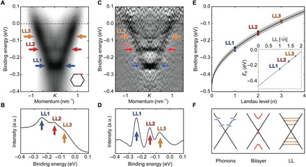
(A) ARPES cut through the Dirac cone at the K point at 300 K. The data have been divided by the Fermi function and symmetrized to compensate for matrix element effects (48). (B) Cut along the energy axis integrated around the K point in (A) in arbitrary units (a.u.). (C) Second derivative of the data in (A) (49). (D) Inverted second derivative of the data shown in (B) after smoothing. (A to D) LLs are indicated by arrows. (E) Summary of LL datasets, with model fit according to Eq. 1 shown in black; the 95% confidence interval of the fit is shown in gray. Different symbols indicate different samples and temperatures: sample A (6 K; hexagons), sample B (6 K; squares), sample B second dataset (6 K; stars), sample B (300 K; diamonds), sample C (6 K; circles), and sample C second dataset (6 K; triangles). ARPES data for the additional samples can be found in fig. S7. Inset: Same data plotted versus , giving the expected linear behavior for LLs in a Dirac material. (F) Sketch of various mechanisms that may lead to ARPES intensity inside the cone. Neither electron-phonon coupling nor contamination from bilayer graphene can explain the experimental findings.
As for other alternative explanations of the data, we note that, while previous ARPES studies of graphene on SiC have shown a rich variety of features (28, 29), the signature spacing of the levels (Fig. 2E, inset) allows us to unambiguously distinguish the observed effect from other possibilities (Fig. 2F). For example, if spectral weight inside the Dirac cone arose from coupling of electrons to phonons (28), it would be limited to characteristic vibrational energies. Similarly, contributions from bilayer and higher-order graphene layers, which can appear in small quantities near step edges of the substrate during the growth process (29) (see also AFM adhesion image in the fig. S9B), would lead to a manifold of bands but would not reproduce the observed band structure (30, 31). Furthermore, previously reported plasmaronic interactions in samples with higher electronic doping (16) can also be excluded. They lead to renormalizations of electronic bands around the Dirac point but show a distinctly different spectrum than what is observed in our experiments. Last, the effects of different defect geometries in graphene and their influence on the Dirac cone dispersion have recently been discussed (32) but do not lead to flat bands around the Dirac point.
To gain deeper insights into the origin of the observed LLs, we model a region of graphene experiencing a uniform strain-induced pseudomagnetic field. We use the simplest such strain pattern, worked out by Guinea et al. (10), which exhibits the triangular symmetry of the underlying honeycomb lattice. Using a tight-binding approach, we directly simulate a finite-size strained region with open boundary conditions and armchair edges (see further details in Materials and Methods). We find that the observed LL spectra can be well reproduced by a triangular flake of side length L = 56 nm (Fig. 3A), subject to a uniform pseudomagnetic field B = 41 T over the entire flake (Fig. 3A). The maximal strain (or relative bond stretching) reaches around 3%, which is in good agreement with our STM measurements. The ARPES data can be simulated by calculating the energy- and momentum-resolved spectral function A(k, ω) of this triangular flake, here shown in Fig. 3 (B and C). Our simulation reproduces the main features of the ARPES data, namely, levels that (i) follow spacing in energy, (ii) are flat inside the Dirac cone and merge with the linearly dispersing bands, and (iii) become less clearly resolved with increasing index n.
Fig. 3. Model calculation of strain-induced LLs.
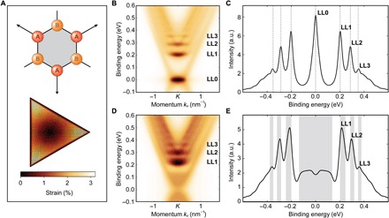
(A) Top: Honeycomb lattice, with the two sublattices A (red) and B (yellow). The black arrows indicate the symmetry of the strain pattern. Bottom: Triangular flake with strain-induced pseudomagnetic field B = 41 T. The color scale indicates the relative bond stretching. (B) Spectral function for the gapless case with Semenoff mass M = 0 meV. (C) Energy cut through the Dirac point (K) of the spectral function in (B). The dashed gray lines indicate the position of the LLs predicted by Eq. 1. (D) Spectral function averaged over a uniform distribution of Semenoff masses M ∈ [−135,135] meV. (E) Energy cut through the Dirac point (K) of the spectral function in (D). The shaded gray area indicates the broadening of the LLs predicted by Eqs. 1 and 2.
Features (ii) and (iii) can be understood by comparing the characteristic size of a Landau orbit (with the magnetic length ) to the length scale λ on which the pseudomagnetic field is uniform. For LLs to exist, an electron on a given Landau orbit must experience a uniform pseudomagnetic field (33), leading to the condition . Hence, for large fields B or large λ, flat bands are expected across the entire Brillouin zone, whereas Dirac cones are recovered in the opposite limit (see fig. S2). The bands observed in the ARPES data can thus be understood as LLs, where the orbit size is only somewhat smaller than λ: By comparing the experimental data and the model calculation, we estimate lB ∼ 4 nm and λ ∼ 30 nm (see Materials and Methods). Furthermore, since the size of Landau orbits grows as , eventually, it becomes comparable to λ, explaining why levels with higher index n are less clearly resolved.
However, our simple model (Fig. 3, B and C) consistently exhibits a sharp zeroth LL (LL0), which is absent in the ARPES data. This discrepancy is unexpected, since LL0 is known to be stable against inhomogeneities of the magnetic field and against disorder, as long as the latter preserves the chiral symmetry of graphene (34). Below, we provide a possible mechanism that broadens LL0 without substantially affecting the higher LLs. It has been argued that graphene grown on SiC is subject to a sublattice symmetry–breaking potential arising from the interaction with the substrate (17). The minimal theoretical model describing this effect, which acts as a staggered potential between sublattices A and B, is the so-called Semenoff mass M (35). This mass term opens a gap at the Dirac point and shifts the LL spectrum for n ≠ 0 to (for a more detailed discussion and the particular case of n = 0, see the Supplementary Materials)
| (2) |
However, a uniform mass term M cannot explain the ARPES data. A fit of the observed LL spectrum to Eq. 2 returns M = (150 ± 5) meV but places the Dirac point at an unrealistic binding energy of EDP = 390 meV (see figs. S3 and S6). Therefore, we postulate that the mass term M varies on a length scale much greater than the magnetic length lB ∼ 4 nm but smaller than the ARPES spot size (∼1 mm). In that situation, our ARPES measurements would simply average over spectral functions described by different mass terms. This is shown in Fig. 3 (D and E) for a uniform distribution in the interval M ∈ [−135,135] meV. As evident from Eq. 2, the distribution of mass terms affects LL0 most while merely contributing an additional broadening to the higher levels. Note that, as observed experimentally, the variation of the mass term is not limited to the strained areas but, instead, is a property of the whole sample; as a result, ARPES always picks up a spatial average of strained areas with LLs and unstrained areas with the usual Dirac cone dispersion, both having the same distribution of mass terms and corresponding Dirac point gaps. This phenomenological model is in good agreement with the experimental data and may renew interest in the variation of the mass term in this sample system (17).
DISCUSSION
This study provides the first demonstration of the room temperature strain-induced QHE in graphene on a wafer-scale platform, as well as the first direct momentum-space visualization of graphene electrons in the strain-induced quantum Hall phase by ARPES, whereby the linear Dirac dispersion collapses into a ladder of quantized LLs. This opens a path for future momentum-resolved studies of strain-induced, room temperature–stable topological phases in a range of materials including Dirac and Weyl semimetals (36–38), monolayer transition metal dichalcogenides (39), and even nodal superconductors (40, 41), all under large, potentially controllable pseudomagnetic fields. These systems will feature time-reversal invariant ground states, otherwise impossible with a true magnetic field, and may act as future building blocks for pseudospin- or valleytronic-based technologies (42). In light of the recently found unconventional superconductivity in “magic angle” bilayer graphene (43, 44), strain-induced pseudomagnetic fields likewise raise the possibility of engineering exotic time-reversal symmetric variants of correlated states including superconductivity in LLs (45) and fractional topological phases (46). Our results lay the foundations for bottom-up strain engineering of novel quantum phases at room temperature and on a technologically relevant wafer-scale platform.
MATERIALS AND METHODS
Sample growth and characterization
Graphene samples with a carbon buffer layer were epitaxially grown on commercial 6H-SiC substrates. The substrates were hydrogen etched before the growth under argon atmosphere. Details are described by Forti and Starke (47). AFM characterization measurements were taken at the Max Planck Institute in Stuttgart. Adhesion images correspond to the force necessary to retract the tip from the sample. Adhesion is sensitive to the graphene coverage on the sample and can thus distinguish between zero layer, monolayer, and bilayer graphene with sensitivity to grain boundaries.
ARPES measurements
Experiments were performed at the University of British Columbia (UBC) in a ultrahigh vacuum chamber equipped with a SPECS Phoibos 150 analyzer with ΔE = 6 meV and optimum energy and momentum resolutions, respectively, at a base pressure of better than p = 7 × 10⁻¹¹ torr. Photons with an energy of 21.2 eV were provided by a SPECS UVS 300 monochromatized gas discharge lamp. Our home-built six-axis cryogenic manipulator allows for measurements between 300 and 3.5 K. Additional datasets were taken at the UBC with a second ARPES setup equipped with a Scienta R4000 analyzer and a Scienta VUV5000 ultraviolet source with ΔE = 1.5 meV and optimum energy and momentum resolutions, respectively, for 21.2-eV photons. The samples were annealed at 600°C for about 2 hours at p = 1 × 10⁻⁹ torr and then at 500°C for about 10 hours at p = 5 × 10⁻¹⁰ torr immediately before the ARPES measurements.
STM measurements
Experiments were performed at the UBC under ultrahigh vacuum conditions (<5 × 10⁻¹² mbar) using a low-temperature scanning tunneling microscope (Scienta Omicron) at liquid helium temperatures (∼4.2 K). All images were acquired in constant-current mode using a cut platinum-iridium tip, which was conditioned by voltage pulsing and gentle indentation into a Ag(111) crystal. The samples were annealed at 550°C overnight with a final pressure of p = 3 × 10⁻¹⁰ mbar in situ before the STM measurements.
Model calculation
We considered a minimal tight-binding model on the honeycomb lattice with nearest-neighbor hoppings and a sublattice symmetry–breaking Semenoff (35) mass term M
| (3) |
where creates an electron in the pz orbital at lattice site r (r′) on the sublattice A (B) of the honeycomb lattice, t = 2.7 eV, and the nearest-neighbor distance is a0 = 0.142 nm. We neglected the electron spin and thus considered effectively spinless fermions.
We constructed a flake in the shape of an equilateral triangle of side length L ∼ 56 nm. The use of armchair edges avoids the zero-energy edge modes appearing for zigzag edges (3). We applied the simplest strain pattern respecting the triangular symmetry of the problem at hand, namely, the pattern introduced by Guinea et al. (10), which gives rise to a uniform (out-of-plane) pseudomagnetic field
| (4) |
where β ≈ 3.37 in graphene (33), and the corresponding displacement field is given by
| (5) |
The hopping parameter renormalization induced by this displacement field was calculated using the simple prescription
| (6) |
where (xij, yij) ≡ ri − rj is the vector joining the original (unstrained) sites i and j and
| (7) |
is the strain tensor corresponding to the (in-plane) displacement field u. Outside the strained region (which we took as a triangle of slightly smaller length LS ∼ 48 nm), we allowed the strain tensor to relax: , where r is the perpendicular distance to the boundary of the strained region and σ ∼ 1 nm. We defined the length scale of the homogeneous magnetic field B to be the diameter of the largest inscribed circle in the triangle of side LS: nm. We stress here that our simulated flakes are much smaller than the experimentally observed triangular features of size ∼300 nm. The fact that we nevertheless reproduced the experimental features underlines how the number of observable LLs is limited by the length scale of the homogeneous pseudomagnetic field λ, rather than by the size L of the nanoprisms themselves. This length scale could be caused by the more complicated strain pattern present in the nanoprisms or be induced by disorder.
We then diagonalized the Hamiltonian (Eq. 3) with hopping parameters given by Eq. 6 to obtain the full set of eigenstates |n〉 with energies En and computed the momentum-resolved, retarded Green’s function using the Lehmann representation
| (8) |
where α = A, B is a sublattice (band) index and η ∼ 20 meV is a small broadening parameter comparable to the experimental resolution.
We then computed the one-particle spectral function
| (9) |
which is proportional to the intensity measured in ARPES (modulo the Fermi-Dirac distribution and dipole matrix elements). We note that using a finite system introduces two main effects in the momentum-resolved spectral function: the appearance of a small finite-size gap at the Dirac points (in the absence of a magnetic field) and a momentum broadening of the bands.
Supplementary Material
Acknowledgments
We gratefully acknowledge C. Ast, G. A. Sawatzky, J. Smet, J. F. Young, Z. Ye, F. Boschini, J. Day, J. Kim, J. Geurs, and C. Li for fruitful discussions. We thank D. Wong for technical assistance and E. Razzoli for support with data processing and analysis. Funding: This research was undertaken thanks, in part, to funding from the Max Planck–UBC–UTokyo Center for Quantum Materials and the Canada First Research Excellence Fund, Quantum Materials and Future Technologies Program. The work at the UBC was supported by the Killam, Alfred P. Sloan, and Natural Sciences and Engineering Research Council of Canada’s (NSERC’s) Steacie Memorial Fellowships (to A.D.); the Alexander von Humboldt Fellowship (to A.D.); the Canada Research Chairs Program (to A.D. and S.A.B.); NSERC; Canada Foundation for Innovation (CFI); British Columbia Knowledge Development Fund (BCKDF); and CIFAR Quantum Materials Program. P.N. thanks the UBC 4YF scholarship and the UBC SBQMI QuEST scholarship for financial support. A.C.Q. and É.L.-H. are supported by the NSERC Alexander Graham Bell Canada Graduate Scholarships–Doctoral (CGS-D) Program. E.M. acknowledges funding from the Swedish Research Council (VR) 2016-06719. Author contributions: P.N. and A.C.Q. performed the ARPES experiments and analyzed the ARPES data. P.N., A.C.Q., E.M., and G.T. performed the STM experiments and analyzed the STM data. É.L.-H. and M.F. provided the theoretical modeling with input from C.G. S.L. and U.S. grew the samples and performed the AFM experiment. P.N., A.C.Q., M.Z., M.M., M.S., S.Z., G.L. provided technical support and maintenance for the ARPES setup. A.D., M.F., S.A.B., D.B., and C.G. supervised the project. P.N., A.C.Q., É.L.-H., and C.G. wrote the manuscript with input from all authors. A.D. was responsible for overall project direction, planning, and management. Competing interests: The authors declare that they have no competing interests. Data and materials availability: All data needed to evaluate the conclusions in the paper are present in the paper and/or the Supplementary Materials. Additional data related to this paper may be requested from the authors.
SUPPLEMENTARY MATERIALS
Supplementary material for this article is available at http://advances.sciencemag.org/cgi/content/full/5/11/eaaw5593/DC1
Fig. S1. Fermi velocity and quasiparticle lifetime from ARPES.
Fig. S2. Evolution of LLs for increasing uniform pseudomagnetic fields.
Fig. S3. Determination of the mass term.
Fig. S4. Sketch of pseudo-LLs with Semenoff mass.
Fig. S5. Calculation of pseudo-LLs with Semenoff mass.
Fig. S6. Model fit with a constant mass term.
Fig. S7. ARPES data on two additional samples.
Fig. S8. AFM height distribution.
Fig. S9. Graphene layer coverage.
REFERENCES AND NOTES
- 1.Novoselov K. S., Jiang D., Schedin F., Booth T. J., Khotkevich V. V., Morozov S. V., Geim A. K., Two-dimensional atomic crystals. Proc. Natl. Acad. Sci. U.S.A. 102, 10451–10453 (2005). [DOI] [PMC free article] [PubMed] [Google Scholar]
- 2.Geim A. K., Novoselov K. S., The rise of graphene. Nat. Mater. 6, 183–191 (2007). [DOI] [PubMed] [Google Scholar]
- 3.Castro Neto A. H., Guinea F., Peres N. M. R., Novoselov K. S., Geim A. K., The electronic properties of graphene. Rev. Mod. Phys. 81, 109–162 (2009). [Google Scholar]
- 4.Anderson M. H., Ensher J. R., Matthews M. R., Wieman C. E., Cornell E. A., Observation of bose-einstein condensation in a dilute atomic vapor. Science 269, 198–201 (1995). [DOI] [PubMed] [Google Scholar]
- 5.Osheroff D. D., Richardson R. C., Lee D. M., Evidence for a new phase of solid He3. Phys. Rev. Lett. 28, 885–888 (1972). [Google Scholar]
- 6.Willett R., Eisenstein J. P., Stoermer H. L., Tsui D. C., Gossard A. C., English J. H., Observation of an even-denominator quantum number in the fractional quantum Hall effect. Phys. Rev. Lett. 59, 1776–1779 (1987). [DOI] [PubMed] [Google Scholar]
- 7.Bardeen J., Cooper L. N., Schrieffer J. R., Phys. Rev. 108, 1175–1204 (1957). [Google Scholar]
- 8.Klitzing K. V., Dorda G., Pepper M., New method for high-accuracy determination of the fine-structure constant based on quantized hall resistance. Phys. Rev. Lett. 45, 494–497 (1980). [Google Scholar]
- 9.Novoselov K. S., Jiang Z., Zhang Y., Morozov S. V., Stormer H. L., Zeitler U., Maan J. C., Boebinger G. S., Kim P., Geim A. K., Room-temperature quantum Hall effect in graphene. Science 315, 1379–1379 (2007). [DOI] [PubMed] [Google Scholar]
- 10.Guinea F., Katsnelson M. I., Geim A. K., Energy gaps and a zero-field quantum Hall effect in graphene by strain engineering. Nat. Phys. 6, 30 (2010). [Google Scholar]
- 11.Levy N., Burke S. A., Meaker K. L., Panlasigui M., Zettl A., Guinea F., Neto A. H. C., Crommie M. F., Strain-induced pseudo magnetic fields greater than 300 tesla in graphene nanobubbles. Science 329, 544–547 (2010). [DOI] [PubMed] [Google Scholar]
- 12.Liu Y., Rodrigues J. N. B., Luo Y. Z., Li L., Carvalho A., Yang M., Laksono E., Lu J., Bao Y., Xu H., Tan S. J. R., Qiu Z., Sow C. H., Feng Y. P., Neto A. H. C., Adam S., Lu J., Loh K. P., Tailoring sample-wide pseudo-magnetic fields on a graphene black phosphorus heterostructure. Nat. Nanotechnol. 13, 828 (2018). [DOI] [PubMed] [Google Scholar]
- 13.Rechtsman M. C., Zeuner J. M., Tuennermann A., Nolte S., Segev M., Szameit A., Strain-induced pseudomagnetic field and photonic Landau levels in dielectric structures. Nat. Photonics 7, 153–158 (2013). [Google Scholar]
- 14.Emtsev K. V., Bostwick A., Horn K., Jobst J., Kellogg G. L., Ley L., McChesney J. L., Ohta T., Reshanov S. A., Rhrl J., Rotenberg E., Schmid A. K., Waldmann D., Weber H. B., Seyller T., Towards wafer-size graphene layers by atmospheric pressure graphitization of silicon carbide. Nat. Mater. 8, 203 (2009). [DOI] [PubMed] [Google Scholar]
- 15.Riedl C., Coletti C., Iwasaki T., Zakharov A. A., Starke U., Quasi-free-standing epitaxial graphene on sic obtained by hydrogen intercalation. Phys. Rev. Lett. 103, 246804 (2009). [DOI] [PubMed] [Google Scholar]
- 16.Bostwick A., Speck F., Seyller T., Horn K., Polini M., Asgari R., MacDonald A. H., Rotenberg E., Observation of plasmarons in quasi-freestanding doped graphene. Science 328, 999–1002 (2010). [DOI] [PubMed] [Google Scholar]
- 17.Zhou S. Y., Gweon G.-H., Fedorov A. V., First P. N., Heer W. A. D., Lee D.-H., Guinea F., Neto A. H. C., Lanzara A., Substrate-induced bandgap opening in epitaxial graphene. Nat. Mater. 6, 770 (2007). [DOI] [PubMed] [Google Scholar]
- 18.Bolen M. L., Harrison S. E., Biedermann L. B., Capano M. A., Graphene formation mechanisms on 4H-SiC(0001). Phys. Rev. B 80, 115433 (2009). [Google Scholar]
- 19.Momeni Pakdehi D., Pierz K., Wundrack S., Aprojanz J., Nguyen T. T. N., Dziomba T., Hohls F., Bakin A., Stosch R., Tegenkamp C., Ahlers F. J., Schumacher H. W., Homogeneous large-area quasi-free-standing monolayer and bilayer graphene on SiC. ACS Applied Nano Materials 2, 844–852 (2019). [Google Scholar]
- 20.Riedl C., Coletti C., Starke U., Structural and electronic properties of epitaxial graphene on SiC (0 0 0 1): A review of growth, characterization, transfer doping and hydrogen intercalation. J. Phys. D. Appl. Phys. 43, 374009 (2010). [Google Scholar]
- 21.Damascelli A., Probing the electronic structure of complex systems by ARPES. Phys. Scr. 2004, 61 (2004). [Google Scholar]
- 22.Hsieh D., Qian D., Wray L., Xia Y., Hor Y. S., Cava R. J., Hasan M. Z., A topological Dirac insulator in a quantum spin Hall phase. Nature 452, 970–974 (2008). [DOI] [PubMed] [Google Scholar]
- 23.Chen Y. L., Analytis J. G., Chu J.-H., Liu Z. K., Mo S.-K., Qi X. L., Zhang H. J., Lu D. H., Dai X., Fang Z., Zhang S. C., Fisher I. R., Hussain Z., Shen Z.-X., Experimental realization of a three-dimensional topological insulator, Bi2te3. Science 325, 178–181 (2009). [DOI] [PubMed] [Google Scholar]
- 24.Lv B. Q., Xu N., Weng H. M., Ma J. Z., Richard P., Huang X. C., Zhao L. X., Chen G. F., Matt C. E., Bisti F., Strocov V. N., Mesot J., Fang Z., Dai X., Qian T., Shi M., Ding H., Observation of Weyl nodes in TaAs. Nat. Phys. 11, 724–727 (2015). [Google Scholar]
- 25.Jang J., Yoo H. M., Pfeiffer L. N., West K. W., Baldwin K. W., Ashoori R. C., Full momentum- and energy-resolved spectral function of a 2d electronic system. Science 358, 901–906 (2017). [DOI] [PubMed] [Google Scholar]
- 26.Bostwick A., Ohta T., Seyller T., Horn K., Rotenberg E., Quasiparticle dynamics in graphene. Nat. Phys. 3, 36–40 (2007). [Google Scholar]
- 27.Song Y. J., Otte A. F., Kuk Y., Hu Y., Torrance D. B., First P. N., de Heer W. A., Min H., Adam S., Stiles M. D., MacDonald A. H., Stroscio J. A., High-resolution tunnelling spectroscopy of a graphene quartet. Nature 467, 185–189 (2010). [DOI] [PubMed] [Google Scholar]
- 28.Ludbrook B. M., Levy G., Nigge P., Zonno M., Schneider M., Dvorak D. J., Veenstra C. N., Zhdanovich S., Wong D., Dosanjh P., Strasser C., Stoehr A., Forti S., Ast C. R., Starke U., Damascelli A., Evidence for superconductivity in Li-decorated monolayer graphene. Proc. Natl. Acad. Sci. 112, 11795–11799 (2015). [DOI] [PMC free article] [PubMed] [Google Scholar]
- 29.Ohta T., Bostwick A., Seyller T., Horn K., Rotenberg E., Controlling the electronic structure of bilayer graphene. Science 313, 951–954 (2006). [DOI] [PubMed] [Google Scholar]
- 30.Ohta T., Bostwick A., McChesney J. L., Seyller T., Horn K., Rotenberg E., Interlayer interaction and electronic screening in multilayer graphene investigated with angle-resolved photoemission spectroscopy. Phys. Rev. Lett. 98, 206802 (2007). [DOI] [PubMed] [Google Scholar]
- 31.Marchenko D., Evtushinsky D. V., Golias E., Varykhalov A., Seyller T., Rader O., Extremely flat band in bilayer graphene. Sci. Adv. 4, eaau0059 (2018). [DOI] [PMC free article] [PubMed] [Google Scholar]
- 32.P. Kot, J. Parnell, S. Habibian, C. Straer, P. M. Ostrovsky, C. R. Ast, Band dispersion of graphene with structural defects. arXiv:1811.00087 (2018).
- 33.Settnes M., Power S. R., Jauho A.-P., Pseudomagnetic fields and triaxial strain in graphene. Phys. Rev. B 93, 035456 (2016). [Google Scholar]
- 34.Aharonov Y., Casher A., Ground state of a spin-onehalf charged particle in a two-dimensional magnetic field. Phys. Rev. A 19, 2461–2462 (1979). [Google Scholar]
- 35.Semenoff G. W., Condensed-matter simulation of a three-dimensional anomaly. Phys. Rev. Lett. 53, 2449–2452 (1984). [Google Scholar]
- 36.Pikulin D., Chen A., Franz M., Chiral anomaly from strain-induced gauge fields in Dirac and Weyl semimetals. Phys. Rev. X 6, 041021 (2016). [Google Scholar]
- 37.Cortijo A., Ferreirs Y., Landsteiner K., Vozmediano M. A., Elastic gauge fields in Weyl semimetals. Phys. Rev. Lett. 115, 177202 (2015). [DOI] [PubMed] [Google Scholar]
- 38.Liu T., Pikulin D. I., Franz M., Quantum oscillations without magnetic field. Phys. Rev. B 95, 041201 (2017). [Google Scholar]
- 39.Rostami H., Roldn R., Cappelluti E., Asgari R., Guinea F., Theory of strain in single-layer transition metal dichalcogenides. Phys. Rev. B 92, 195402 (2015). [Google Scholar]
- 40.Massarelli G., Wachtel G., Wei J. Y. T., Paramekanti A., Pseudo-Landau levels of Bogoliubov quasiparticles in strained nodal superconductors. Phys. Rev. B 96, 224516 (2017). [Google Scholar]
- 41.Nica E. M., Franz M., Landau levels from neutral Bogoliubov particles in two-dimensional nodal superconductors under strain and doping gradients. Phys. Rev. B 97, 024520 (2018). [Google Scholar]
- 42.Low T., Guinea F., Strain-induced pseudomagnetic field for novel graphene electronics. Nano Lett. 10, 3551–3554 (2010). [DOI] [PubMed] [Google Scholar]
- 43.Cao Y., Fatemi V., Demir A., Fang S., Tomarken S. L., Luo J. Y., Sanchez-Yamagishi J. D., Watanabe K., Taniguchi T., Kaxiras E., Ashoori R. C., Jarillo-Herrero P., Correlated insulator behaviour at half-filling in magic-angle graphene superlattices. Nature 556, 80–84 (2018). [DOI] [PubMed] [Google Scholar]
- 44.Cao Y., Fatemi V., Fang S., Watanabe K., Taniguchi T., Kaxiras E., Jarillo-Herrero P., Unconventional superconductivity in magic-angle graphene superlattices. Nature 556, 43–50 (2018). [DOI] [PubMed] [Google Scholar]
- 45.Uchoa B., Barlas Y., Superconducting states in pseudo-Landau-levels of strained graphene. Phys. Rev. Lett. 111, 046604 (2013). [DOI] [PubMed] [Google Scholar]
- 46.Ghaemi P., Cayssol J., Sheng D. N., Vishwanath A., Fractional topological phases and broken time-reversal symmetry in strained graphene. Phys. Rev. Lett. 108, 266801 (2012). [DOI] [PubMed] [Google Scholar]
- 47.Forti S., Starke U., Epitaxial graphene on SiC: From carrier density engineering to quasi-free standing graphene by atomic intercalation. J. Phys. D. Appl. Phys. 47, 094013 (2014). [Google Scholar]
- 48.Shirley E. L., Terminello L. J., Santoni A., Himpsel F. J., Brillouin-zone-selection effects in graphite photoelectron angular distributions. Phys. Rev. B 51, 13614–13622 (1995). [DOI] [PubMed] [Google Scholar]
- 49.Zhang P., Richard P., Qian T., Xu Y.-M., Dai X., Ding H., A precise method for visualizing dispersive features in image plots. Rev. Sci. Instrum. 82, 043712 (2011). [DOI] [PubMed] [Google Scholar]
- 50.Hunt B., Sanchez-Yamagishi J. D., Young A. F., Yankowitz M., LeRoy B. J., Watanabe K., Taniguchi T., Moon P., Koshino M., Jarillo-Herrero P., Ashoori R. C., Massive Dirac fermions and Hofstadter butterfly in a van der Waals heterostructure. Science 340, 1427–1430 (2013). [DOI] [PubMed] [Google Scholar]
- 51.Emtsev K. V., Speck F., Seyller T., Ley L., Riley J. D., Interaction, growth, and ordering of epitaxial graphene on SiC{0001} surfaces: A comparative photoelectron spectroscopy study. Phys. Rev. B 77, 155303 (2008). [Google Scholar]
- 52.Virojanadara C., Syvjarvi M., Yakimova R., Johansson L. I., Zakharov A. A., Balasubramanian T., Homogeneous large-area graphene layer growth on 6h-SiC(0001). Phys. Rev. B 78, 245403 (2008). [Google Scholar]
Associated Data
This section collects any data citations, data availability statements, or supplementary materials included in this article.
Supplementary Materials
Supplementary material for this article is available at http://advances.sciencemag.org/cgi/content/full/5/11/eaaw5593/DC1
Fig. S1. Fermi velocity and quasiparticle lifetime from ARPES.
Fig. S2. Evolution of LLs for increasing uniform pseudomagnetic fields.
Fig. S3. Determination of the mass term.
Fig. S4. Sketch of pseudo-LLs with Semenoff mass.
Fig. S5. Calculation of pseudo-LLs with Semenoff mass.
Fig. S6. Model fit with a constant mass term.
Fig. S7. ARPES data on two additional samples.
Fig. S8. AFM height distribution.
Fig. S9. Graphene layer coverage.