Abstract
2D van der Waals layered heterostructures allow for a variety of energy band offsets, which help in developing valuable multifunctional devices. However, p–n diodes, which are typical and versatile, are still limited by the material choice due to the fixed band structures. Here, the vanadium dopant concentration is modulated in monolayer WSe2 via chemical vapor deposition to demonstrate tunable multifunctional quantum tunneling diodes by vertically stacking SnSe2 layers at room temperature. This is implemented by substituting tungsten atoms with vanadium atoms in WSe2 to provoke the p‐type doping effect in order to efficiently modulate the Fermi level. The precise control of the vanadium doping concentration is the key to achieving the desired quantum tunneling diode behaviors by tuning the proper band alignment for charge transfer across the heterostructure. By constructing a p–n diode for p‐type V‐doped WSe2 and heavily degenerate n‐type SnSe2, the type‐II band alignment at low V‐doping concentration is clearly shown, which evolves into the type‐III broken‐gap alignment at heavy V‐doping concentration to reveal a variety of diode behaviors such as forward diode, backward diode, negative differential resistance, and ohmic resistance.
Keywords: 2D tunneling heterojunctions, chemical vapor deposition, functional diodes, tin diselenide, vanadium‐doped tungsten diselenide
2D multifunctional diodes are realized by stacking CVD‐grown V‐doped WSe2 monolayers (p‐type) and SnSe2 (n‐type). Substituting W‐atoms with V‐atoms in WSe2 provokes the p‐type doping effect to modulate the Fermi level. The type‐II band alignment evolves into the type‐III broken‐gap alignment with increasing V‐doping concentration, revealing various diode behaviors such as forward, backward, and especially negative differential resistance transport.
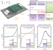
2D van der Waals (vdW) layered semiconductors possess various bandgaps ranging from 0.4 to 2.0 eV and different electron affinities, establishing predetermined heterojunctions of type‐I (straddling gap), type‐II (staggered gap), or type‐III (broken gap) band alignments.1, 2, 3, 4 Accordingly, a variety of functional devices can be developed by taking advantage of p–n junctions with different band alignments, which are the elementary building blocks for numerous applications in diodes, transistors, photodetectors, and solar cells.5, 6, 7, 8, 9 In addition, the charge transfer originating from the thermionic emission or quantum tunneling is affected by the band bending near the heterojunction, which relies on the Fermi level difference between materials.
Previously, carrier transport properties through a heterojunction appear to be in principle material‐dependent behaviors. Recent reports show the possibility to integrate multiple functions in a certain vdW heterostructure; for example, black phosphorus (BP) of different thicknesses are employed to provide a tunable Fermi level for the desired band bending.10, 11 Nevertheless, BP suffers from sensitivity in air.12 Besides, the use of mechanically exfoliated BP is not tenable for controlling the exact flake thickness, which directly determines its Fermi level, let alone realize accessible integration.
Chemical vapor deposition (CVD) technique is a promising approach in a wafer‐scale synthesis for industrial applications. Moreover, introducing the dopant during CVD growth is an effective way to change the carrier density in the material and thus modulate the position of the Fermi level.13 Here, we report a reliable and repeatable method to synthesize vanadium (V) substituted WSe2 monolayer by CVD and demonstrate multifunctional p–n diode behaviors in V‐doped WSe2/SnSe2 heterostructures. A liquid precursor with tungsten host and vanadium dopant atoms is adopted in our approach with only two zones for the precise control of V‐doping concentration in WSe2. The coverage of the grown‐WSe2 flakes is increased up to 90% at a high liquid precursor concentration (Figure S1, Supporting Information). In addition to the p‐type V‐doped WSe2 monolayer, multilayer SnSe2 as an n‐type material is introduced to construct the p–n junction. We observe the diverse p–n diode behaviors in V‐WSe2/SnSe2 devices with various V‐doping concentrations at room temperature, including quantum tunneling p–n diodes for the forward rectification, backward rectification, negative differential resistance (NDR), and ohmic resistance.
Figure 1 a,b is the schematics for synthesizing V‐doped WSe2 monolayer with the CVD approach. Liquid precursor containing solutions of ammonium metatungstate (AMT: W‐precursor) and ammonium metavanadate (AMV: V‐precursor) together with a promoter of alkali metal (NaOH) and iodixanol is spin‐casted on SiO2/Si substrate and then introduced into a two‐zone furnace CVD for the selenization process. The molar ratio of AMT to AMV in the liquid precursor is precisely controlled using a micropipette.
Figure 1.
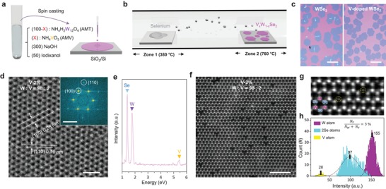
Synthesis and atomic structure of monolayer V‐doped WSe2. a) Schematic for preparation process of water‐based precursor. The precursor containing sodium metal (promoter), ammonium tungstate (W‐precursor), and ammonium vanadate (V‐precursor) are spin‐casted onto SiO2/Si wafer. b) Two‐zone furnace CVD process for growing V‐doped WSe2. The precursor‐coated substrate is introduced into the CVD chamber and is followed by selenization. c) Optical images of pure and V‐doped WSe2. The monolayer (0.8 nm) was retained up to V‐10% doping. The scale bar is 150 µm. d,e) High‐resolution TEM image (d) and EDS spectrum (e) of V‐2% WSe2. The scale bar is 1 nm. f,g) Unfiltered (f) and Gaussian‐filtered (g) ADF‐STEM images of V‐2% WSe2. After the filtering process, the substituted V atoms in W sites are clealy seen. The scale bar is 2 nm. h) The number of W, Se, and V atoms with the STEM intensity. The scale bar is 1 nm.
The hexagonal shape of flakes is preserved in V‐doped WSe2 samples (up to V‐10%), similar to the pristine WSe2 flakes (Figure 1c; Figure S2, Supporting Information). The V‐10% sample shows a uniform contrast in the entire flake area with a height profile of 0.8 nm, confirmed by atomic force microscope (AFM). The monolayer is maintained up to V‐10% doping (Figure S2, Supporting Information), at which multilayers are partially spotted. The highly crystalline atomic structure of V‐doped WSe2 monolayer (V‐2%) is observed without noticeable defect sites from the high‐resolution transmission electron microscopy (HRTEM) image with selective‐area electron‐diffraction pattern (Figure 1d). The interlayer distances of the (100) and (110) planes are identified to be 0.28 and 0.16 nm, respectively, in consistent with the reported values in WSe2.14
To explore V‐incorporation in WSe2, we further performed energy‐dispersive X‐ray (EDX) spectroscopy and annular dark field scanning TEM (ADF‐STEM). The chemical elements of V atom in addition to W and Se atoms were clearly discernible in EDX spectrum (Figure 1e) and EDX mapping (Figure S3, Supporting Information). Unlike the HRTEM image in Figure 1d, numerous dark spots are clearly distinguished in ADF‐STEM image (Figure 1f). The intensity of STEM is proportional to the atomic number (AN) by a*(AN)x, where a is constant and x ranges from 1.5 to 2.5.15 Therefore, the lowest atomic number of V (AN = 23) atoms are seen as the dark spots compared with brightest W (AN = 74) and Se (AN = 34) atoms. After Gaussian filtering (Figure 1g), V atoms are clearly seen by substituting W atoms. The average intensities of W (155), 2Se (97), and V (28) atoms are well fitted to a*(AN)x (a = 0.29, x = 1.55), indicating that the dark spots are indeed V atoms (Figure 1h). Se‐vacancies are also presented in Figure S4 of the Supporting Information with a vacancy density of 1.7 × 1013 cm−2.
Figure 2 a demonstrates the Raman spectra of V‐doped WSe2 with different V‐doping concentrations (Figure S5, Supporting Information). The Raman shift near 250 cm−1 is ascribed to the mixed modes of E1 2g (strain) with A1g (charge transfer) and is red‐shifted to 3 cm−1 at 4% V‐doping concentration. Such a red‐shift is dominantly ascribed to the A1g mode by the p‐doping effect of V atoms on WSe2.16 The 2LA(M) mode appears around 260 cm−1 and is gradually developed as V‐doping concentration increases, reflecting the emergent crystalline disorders due to the randomly distributed V atoms.17 The photoluminescence (PL) is further conducted to study the p‐doping effect of V‐substitution to WSe2 (Figure 2b). The asymmetric PL emission near 1.66 eV is reminiscent of the positive trions in intrinsic p‐doped WSe2 (trion binding energy = ≈30 meV).18 As V‐doping concentration increases, the PL intensity is reduced due to charge (hole) screening and the position is red‐shifted by the developed positive trions.19
Figure 2.
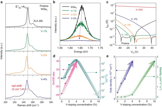
p‐Doping effect of V‐substitution to WSe2. a,b) Raman (a) and PL (b) spectra of V‐doped WSe2 monolayer at an excitation wavelength of 532 nm in terms of V‐doping concentration. c) I DS–V G curves of V‐doped WSe2 transistors under V DS = 0.5 V. d,e) On/off ratio (I −50 V/I off) and threshold voltage (d) field‐effect hole mobility and intrinsic hole carrier concentration (e) as a function of V‐doping concentration.
To investigate V‐doping effect on the electrical performance, we fabricated field effect transistors (FETs) using V‐doped WSe2 with Pd contact electrodes for efficient hole transport (Figure 2c). The pristine WSe2‐FET shows ambipolar transfer characteristics at a drain bias of 0.5 V. This prevails the p‐type behavior as V‐doping concentration increases. The threshold voltage in the hole region is shifted to the positive side, while the on/off current ratio reaches to ≈105 at V‐4% doping (Figure 2d). At a high V‐doping concentration of 10%, the FET shows a heavily degenerate behavior with a negligible current modulation within the entire range of gate voltages (−50 to 50 V). Moreover, the hole mobility and carrier density increase as a function of V‐doping concentration (Figure 2e; for the detail calculation, see Note S1 and S2, and Figure S6, Supporting Information).
We next construct two‐terminal p–n diodes by vertically stacking the grown V‐doped WSe2 as a p‐type and the exfoliated SnSe2 as an n‐type, as shown schematically (Figure 3 a). The source and drain electrodes of Pd are deposited on the V‐WSe2/SnSe2 heterostructure (Figure 3b; for the detail fabrication process, see Figure S7, Supporting Information).20, 21 The thickness of SnSe2 flakes in all diodes were 11–17 nm, as confirmed by AFM for the controlled experiments (Figure S8, Supporting Information). The Fermi level of the V‐doped WSe2 is modulated with V‐doping concentration. Meanwhile, the multilayer SnSe2 FET device reveals a heavily degenerate n‐type behavior by the high n‐type current of ≈100 µA µm−1 (Figure S8, Supporting Information). As V‐doping concentration increases, the Fermi level is shifted toward the valence band edge up to V‐4% and further into the valence band at V‐10%, implying a near broken‐gap band alignment with n‐type SnSe2 (Figure 3c).22
Figure 3.
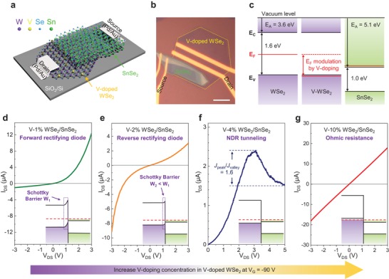
Device structure and electrical performance of two‐terminal diodes from CVD‐synthesized V‐doped WSe2 and exfoliated SnSe2. a) Schematic showing p‐type V‐WSe2 at the bottom and n‐type SnSe2 on top, with both Pd contacts. b) Optical image of a representative device of V‐2%. The scale bar is 10 µm. c) Band structures of V‐WSe2 and SnSe2 with their electron affinities and bandgaps, suggesting near broken‐gap alignment in the heterostructures. The Fermi levels are estimated from the threshold voltages. d–g) I DS–V DS characteristics (linear scale at room temperature) with diverse diode behaviors corresponding to different V‐doping concentrations in WSe2. The inset figures are the band alignments simulated by Poisson's equation when SnSe2 was brought into contact with V‐doped WSe2. All the devices are gated at −90 V.
We now demonstrate a variety of diode behaviors in V‐WSe2/SnSe2 devices by varying the V‐doping concentration at room temperature. The diode device at V‐1% (Figure 3d) as well as the pristine WSe2 device (Figure S9, Supporting Information) shows a typical forward rectifying diode behavior. The Fermi level of V‐1% or pristine WSe2 sample locates near the middle of the bandgap, allowing for a large current flow from WSe2 to SnSe2 driven by the forward bias while suppressing the reverse current. At V‐2% doping, the Fermi level downshifts closer to the valence band. An asymmetric ambipolar transistor is manifested, preferring a backward rectifying diode behavior (Figure 3e). A more prominent device is constructed at V‐4% doping. NDR behavior is clearly observed in the forward bias region from 2.8 to 5.0 V with a peak‐to‐valley ratio of 1.6 (Figure 3f). When the Fermi level of n‐SnSe2 is located above the valence band edge of V‐doped WSe2, the current drops gradually with the reduction in electron band‐to‐band tunneling (BTBT). At a high V‐doping concentration (V‐10%), the V‐doped WSe2 turns into the degenerate state with the Fermi level getting inside the valence band, which is confirmed by the subtle gating effect in the entire range of gate bias (Figure S10, Supporting Information). In such a case, the diode behaves as an ohmic resistance due to the presence of both degenerate n‐SnSe2 and degenerate p‐WSe2 (Figure 3g). The contact issues of resistance are excluded here owing to the near‐ohmic contact in V‐doped WSe2/Pd junctions (Figure S11, Supporting Information).10
The band bending of alignments in heterostructures occurs in planar V‐doped WSe2 rather than the vertical V‐WSe2/SnSe2 junction due to the thin thickness of monolayer V‐WSe2 9, 23 and low carrier density while the V‐doping concentration is low. In view of the SnSe2, which is degenerate and appears in metal, the band bending can be negligible. According to Poisson's equation, band alignments in the V‐WSe2/SnSe2 heterojunctions are calculated upon different V‐doping concentrations in V‐doped WSe2 (insets in Figure 3d–g; the details are provided in Note S3 and Figure S12, Supporting Information). The band bending (depletion region width) in the V‐WSe2 at low V‐doping concentration are much longer than the atomic thickness of monolayer V‐WSe2, inducing the bands bend along the planar direction in V‐WSe2. The initial type II band alignment is preserved at low V‐concentration (up to V‐4%). Further increase V‐concentration to V‐10%, the width of the depletion layer decreases, eventually obtains a type III broken‐gap alignment, implying the evolution of the carrier transport mechanism.
The aforementioned appealing device characteristics modulated by V‐doping concentration are further improved for high device efficiency via electrostatic doping. The I DS–V DS output curves are measured at various gate biases from −30 to −110 V (Figure 4 ). In addition to the p‐type V‐doping in WSe2, the hole doping by the negative gate bias is applied to boost the efficiency without altering the device characteristics.24, 25 The Fermi level in heavily n‐doped SnSe2 is strongly pinned. In the forward rectifying diode at 1% V‐WSe2 (Figure 4a), a high current is achieved at a large negative gate bias; however, it yields a high rectification ratio (I 3V/I −3 V) of 135 at V G = −30 V, benefiting from the suppression of minority carrier drift in the off‐state compared to that at V G = −110 V. For the backward rectifying diode, the rectification ratio (I −3 V/I 3V) increases up to 2.8 at V G = −110 V (Figure 4b). Meanwhile, the peak‐to‐valley ratio in NDR diode rises up to 2.3 at V G = −110 V (Figure 4c). Similar device characteristics are obtained from other four devices with the corresponding V‐doping concentration (Figure S13, Supporting Information). Figure 4d summarizes the improved device performances in terms of the rectification ratio (forward and backward) and peak‐to‐valley ratio with the gate bias modulation. The reproducibility of our devices is ensured with reasonable error bars. As the negative gate bias increases, the rectification ratio degrades in the forward direction but is improved in the backward diode. The peak‐to‐valley ratio is inversely proportional to the gate bias with a maximum value of 2.3, especially with 4% V‐WSe2, higher than the value of 1.8 obtained from the WSe2/SnSe2 without h‐BN insulating layer.26 This is ascribed to the increase in available energy states for tunneling, modulated by the high V‐doping concentration.
Figure 4.
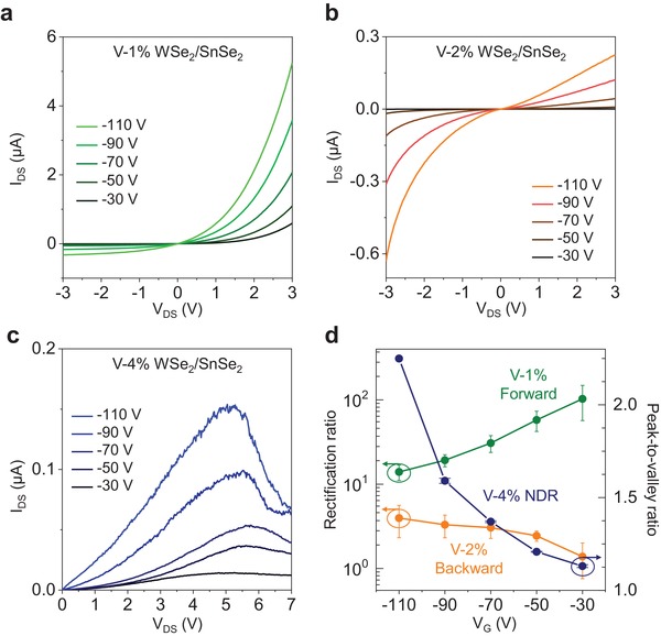
Gate‐tunable behaviors of V‐doped WSe2/SnSe2 devices. a–c) I DS–V DS output curves of the forward rectifying diode, backward rectifying diode, and NDR tunneling under various gate biases. d) Device rectification ratio (I 3V/I −3 V in the forward direction, and I −3 V/I 3V in the backward direction) and NDR peak‐to‐valley ratio as a function of gate bias with reasonable error bars, demonstrating the reproducibility.
Diverse diode behaviors indicate different carrier transport mechanisms. In the pristine WSe2 or V‐1% device, there is a depletion region in WSe2 nearby the heterointerfaces (Figure S12a, Supporting Information). Under a positive drain bias (Figure 5 a), the energy bands of WSe2 shift down, thinning the barrier width. The majority electrons residing in the SnSe2 conduction band, therefore, overcome the triangular barrier and migrate to the other side, generating a forward current. This process is dominated by the thermionic Fowler–Nordheim (FN) tunneling or FN tunneling, which can be modeled as27
| (1) |
where A is the effective contact area, q is the unit charge, h is the Planck's constant, m and m* are the electron free mass and effective mass, respectively, and W and φ are the barrier width and height, respectively. Based on the derivation, 1/V follows ln(I/V 2) in the relationship of negative linear correlation. The ln(I/V 2)‐1/V plot (Figure S14, Supporting Information) is calculated from Figure 3d, confirming FN tunneling mechanism with the negative slop at a high drain bias (near zero).28 When V DS < 0, the minority carrier drift starts to dominate the current flowing from SnSe2 to WSe2. Since the intrinsic concentration of minority carriers is limited and the diffusion length stays identical, the reverse current is small and tends to saturate, showing a forward rectifying behavior.
Figure 5.
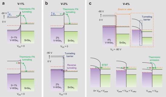
Band alignments in various V‐doped WSe2/SnSe2 devices. a) In the pristine WSe2 and V‐1% devices, driven by a positive drain bias, the majority electrons thermally excited from the SnSe2 conduction band dominate the carrier transport via FN tunneling, generating a forward rectifying current. ϕa is the built‐in potential. b) In the V‐2% device, when V DS < 0, electrons tunnel from the WSe2 valence band into the empty conduction band of SnSe2 by the band‐to‐band tunneling, exhibiting a backward rectifying behavior. ϕb is the built‐in potential. c) In the V‐4% WSe2, the Fermi level is expected to enter its valence band at a high negative gate due to the strong accumulation of holes. A tunneling channel is thereby established in the device for the band‐to‐band tunneling. Electrons are transferred across the tunneling barrier at the interface with an NDR behavior in the positive drain bias region.
The Fermi level in V‐2% WSe2 locates closer to its valence band edge compared to that in pristine or V‐1% sample because of the V‐doping effect, and further approaches at a high negative gate bias. When V DS > 0, the SnSe2 conduction band aligns with the forbidden band of WSe2, resulting in the forward FN tunneling current as in pristine WSe2 or V‐1% device (upper panel in Figure 5b). The depletion region in V‐2% WSe2 is much thinner but the built‐in potential shows ϕb < ϕa (marked in upper panels in Figure 5b and Figure 5a, respectively) as indicated in the calculated band alignment (Figure S12b, Supporting Information), leading to a smaller forward current. Meanwhile, the energy bands of V‐WSe2 move upward when V DS < 0, which allows for electrons from the WSe2 valence band heading to the empty states in the SnSe2 conduction band, generating a backward BTBT current. In this case, the thinner tunneling barrier promotes the efficient band‐to‐band tunneling in backward, whereas the lower built‐in potential reduces the forward thermionic current, forming the backward rectifying behavior.
As V‐4% WSe2‐FET shows a strong p‐type property, the original Fermi level is expected to locate near its valence band edge (Figure S12c, Supporting Information). Gated by a high negative bias (Figure 5c), the electrostatic doping pushes the Fermi level into the valence band due to the strong accumulation of holes, leaving large amounts of empty states. Driven by a small positive drain bias (0 < V DS < V peak), electrons from the SnSe2 conduction band tunnel into the WSe2 valence band owing to the overlap of equivalent energy states, and thus the forward tunneling current is generated. This current then reaches its peak when the SnSe2 Fermi level matches the WSe2 valence band edge, where the populations of equivalent states in two sides reach a maximum. A further increase in V DS induces the reduction in the tunneling current, namely, NDR behavior. The upper part of the SnSe2 conduction band aligns with the forbidden band of WSe2, thereby prohibiting the BTBT of electrons, and the overlap region shrinks continuously until vanishes. Normally, I DS would pick up after the valley point and be dominated by the thermionic emission. However, this part is absent in some of our devices, which is probably because of the tunneling barrier or large hysteresis. Most of the drain bias drops at the wide interface barrier, which results in the appearance of peak current at a high V DS. In addition, the large hysteresis in the V‐4% WSe2 transistor (Figure S15a, Supporting Information) indicates the carrier trapping or scattering, which severely impedes the majority carrier diffusion. Apart from this, device with apparent I DS pick‐up behavior is provided in Figure S15b of the Supporting Information with a peak‐to‐valley ratio of 1.4.
In conclusion, we have shown the tunable quantum tunneling in the V‐doped WSe2/SnSe2 heterostructure by varying the doping concentration at room temperature. A liquid precursor containing transition metal and vanadium dopant atoms is used in our approach to synthesize V‐WSe2 via CVD. The precise control of the doping concentration efficiently modulates the Fermi level position, achieving the p‐type doping effect. This method induces the substitution of W by V, endowing a proper band bending for the desired band alignment, which determines the charge transfer across the heterostructure. We theoretically probed the variation in the band alignment upon to different V‐doping concentration, where the intrinsic type‐II band alignment is preserved at low concentration, and evolves into the type‐III broken‐gap alignment by heavily doping. Hence, the realization of diverse functions with the forward rectifying diode, backward rectifying diode, NDR diode, and ohmic resistance has been illustrated. They therefore suggest the promising opportunities to be applied for future integration in the scaled electronics.
Experimental Section
Preparation of Liquid Precursor: The precursor solution was prepared by mixing four types of water‐based solutions: (i) tungsten precursor (ammonium metatungstate: NH4H2W12O4), (ii) vanadium precursor (ammonium metavanadate: NH4VO3), (iii) promoter (sodium hydroxide: NaOH), and (iv) medium solution (iodixanol). The V‐doping concentration in V‐doped WSe2 was adjusted by mixing the molar ratio of tungsten to vanadium precursor. The mixed solution was then coated onto SiO2/Si wafer by spin‐casting at 3000 rpm for 1 min.
Synthesis of V‐Doped WSe2 by CVD: An atmospheric CVD system with two‐zone furnaces was used for separately controlling the temperature of the selenium source and reaction zone. Here, 0.5 g of selenium (Sigma, 209643) was introduced, while the precursor‐coated substrate was placed in the reaction zone. For the growth of V‐doped WSe2, the selenium zone was heated up to 400 °C at a rate of 50 °C per min. At the same time, the substrate zone was set to 760 °C. Nitrogen gas of 500 sccm and hydrogen gas of 25 sccm were injected during CVD.
TEM Measurement: TEM and ADF‐STEM images were taken by a probe aberration‐corrected JEM ARM 200F machine, operated at 80 kV for high‐resolution TEM observations. The imaging time was set within 1 min under a high‐magnification STEM node to avoid beam damage on the monolayer V‐doped WSe2 samples.
Device Fabrication: The fabrication of the V‐WSe2/SnSe2 devices consists of three steps: (i) pristine WSe2 or V‐WSe2 flakes transfer, (ii) exfoliation of SnSe2 flakes and dry transfer in the glovebox, and (iii) electrode metallization. First, the CVD grown WSe2 flakes were transferred onto a 300 nm SiO2/Si substrate by wet‐etching using hydrofluoric acid. Second, the SnSe2 flakes were exfoliated using a Scotch tape onto a poly propylene carbonate (PPC)/300 nm SiO2/Si substrate, visualizing the thin and large‐size flakes. The desired SnSe2 flake along with the PPC film was then mechanically peeled off from the silicon substrate and attached onto a polydimethylsiloxane stamp. Next, SnSe2 and WSe2 were brought together, followed by poly methyl methacrylate spin‐coating prior to performing electrode metallization for protection. All the manipulations of SnSe2 flakes were performed in the glovebox. Finally, the source (S) and drain (D) contacts (Pd/Au of 5/50 nm) for both WSe2 and SnSe2 were patterned by e‐beam lithography prior to metal deposition. The entire fabrication process was schematically illustrated in Figure S7 of the Supporting Information.
Device Characterization: Electrical measurements were conducted by a probe station equipped with source/measurement units (Keithley 4200 and Agilent B2900A) at the high vacuum (10−6 Torr). AFM mapping analyses were recorded in a SPA400 (SEIKO) system. NT‐MDT Raman & PL spectroscopy (532 nm laser) were used to study the samples.
Conflict of Interest
The authors declare no conflict of interest.
Supporting information
Supporting Information
Acknowledgements
S.F. and S.J.Y. contributed equally to this work. This work was supported by the Institute for Basic Science of Korea (IBS‐R011‐D1).
Fan S., Yun S. J., Yu W. J., Lee Y. H., Tailoring Quantum Tunneling in a Vanadium‐Doped WSe2/SnSe2 Heterostructure. Adv. Sci. 2020, 7, 1902751 10.1002/advs.201902751
References
- 1. Shim J., Oh S., Kang D., Jo S., Ali M. H., Choi W., Heo K., Jeon J., Lee S., Kim M., Song Y. J., Park J., Nat. Commun. 2016, 7, 13413. [DOI] [PMC free article] [PubMed] [Google Scholar]
- 2. Hong X., Kim J., Shi S., Zhang Y., Jin C., Sun Y., Tongay S., Wu J., Zhang Y., Wang F., Nat. Nanotechnol. 2014, 9, 682. [DOI] [PubMed] [Google Scholar]
- 3. Li M., Bellus M. Z., Dai J., Ma L., Li X., Zhao H., Zeng X. C., Nanotechnology 2018, 29, 335203. [DOI] [PubMed] [Google Scholar]
- 4. Fang H., Battaglia C., Carraroc C., Nemsak S., Ozdol B., Kang J. S., Bechtel H. A., Desai S. B., Kronast F., Unal A. A., Conti G., Conlon C., Palsson G. K., Martin M. C., Minor A. M., Fadley C. S., Yablonovitch E., Maboudian R., Javey A., Proc. Natl. Acad. Sci. USA 2014, 111, 6198. [DOI] [PMC free article] [PubMed] [Google Scholar]
- 5. Cheng R., Li D., Zhou H., Wang C., Yin A., Jiang S., Liu Y., Chen Y., Huang Y., Duan X., Nano Lett. 2014, 14, 5590. [DOI] [PMC free article] [PubMed] [Google Scholar]
- 6. Britnell L., Ribeiro R. M., Eckmann A., Jalil R., Belle B. D., Mishchenko A., Kim Y., Gorbachev R. V, Georgiou T., Morozov S. V, Grigorenko A. N., Geim A. K., Casiraghi C., Neto A. H. C., Novoselov K. S., Science 2013, 340, 1311. [DOI] [PubMed] [Google Scholar]
- 7. Yu W. J., Liu Y., Zhou H., Yin A., Li Z., Huang Y., Duan X., Nat. Nanotechnol. 2013, 8, 952. [DOI] [PMC free article] [PubMed] [Google Scholar]
- 8. Yu W. J., Li Z., Zhou H., Chen Y., Wang Y., Huang Y., Duan X., Nat. Mater. 2013, 12, 246. [DOI] [PMC free article] [PubMed] [Google Scholar]
- 9. Lee C., Lee G., Van Der Zande A. M., Chen W., Li Y., Han M., Cui X., Arefe G., Nuckolls C., Heinz T. F., Guo J., Hone J., Kim P., Nat. Nanotechnol. 2014, 9, 676. [DOI] [PubMed] [Google Scholar]
- 10. Liu X., Qu D., Li H., Moon I., Ahmed F., Kim C., Lee M., Choi Y., Cho J. H., Hone J. C., Yoo W. J., ACS Nano 2017, 11, 9143. [DOI] [PubMed] [Google Scholar]
- 11. Srivastava P. K., Hassan Y., Gebredingle Y., Jung J., Kang B., Yoo W. J., Singh B., Lee C., Small 2019, 15, 1804885. [DOI] [PubMed] [Google Scholar]
- 12. Wang Y., Yang B., Wan B., Xi X., Zeng Z., Liu E., Wu G., Liu Z., Wang W., 2D Mater. 2016, 3, 035025. [Google Scholar]
- 13. Yun S. J., Han G. H., Kim H., Duong D. L., Shin B. G., Zhao J., Vu Q. A., Lee J., Lee S. M., Lee Y. H., Nat. Commun. 2017, 8, 2163. [DOI] [PMC free article] [PubMed] [Google Scholar]
- 14. Yun S. J., Kim S. M., Kim K. K., Lee Y. H., Curr. Appl. Phys. 2016, 16, 1216. [Google Scholar]
- 15. Yamashita S., Kikkawa J., Yanagisawa K., Nagai T., Ishizuka K., Kimoto K., Sci. Rep. 2018, 8, 12325. [DOI] [PMC free article] [PubMed] [Google Scholar]
- 16. Chen C.‐H., Wu C.‐L., Pu J., Chiu M. H., Kumar P., Takenobu T., Li L.‐J., 2D Mater. 2014, 1, 034001. [Google Scholar]
- 17. Mignuzzi S., Pollard A. J., Bonini N., Brennan B., Gilmore I. S., Pimenta M. A., Richards D., Roy D., Phys. Rev. B 2015, 91, 195411. [Google Scholar]
- 18. Wang G., Bouet L., Lagarde D., Vidal M., Balocchi A., Amand T., Marie X., Urbaszek B., Phys. Rev. B 2014, 90, 075413. [DOI] [PubMed] [Google Scholar]
- 19. Kang W. T., Lee I. M., Yun S. J., Il Song Y., Kim K., Kim D. H., Shin Y. S., Lee K., Heo J., Kim Y. M., Lee Y. H., Yu W. J., Nanoscale 2018, 10, 11397. [DOI] [PubMed] [Google Scholar]
- 20. Wang Y., Yang R. X., Quhe R., Zhong H., Cong L., Ye M., Ni Z., Song Z., Yang J., Shi J., Li J., Lu J., Nanoscale 2016, 8, 1179. [DOI] [PubMed] [Google Scholar]
- 21. Fang H., Chuang S., Chang T. C., Takei K., Takahashi T., Javey A., Nano Lett. 2012, 12, 3788. [DOI] [PubMed] [Google Scholar]
- 22. Zhang C., Gong C., Nie Y., Min K., Liang C., Oh Y. J., Zhang H., Wang W., Hong S., Colombo L., Wallace R. M., Cho K., 2D Mater. 2017, 4, 015026. [Google Scholar]
- 23. Nourbakhsh A., Zubair A., Dresselhaus M. S., Palacios T., Nano Lett. 2016, 16, 1359. [DOI] [PubMed] [Google Scholar]
- 24. Zhou X., Hu X., Zhou S., Song H., Zhang Q., Pi L., Li L., Li H., Lü J., Zhai T., Adv. Mater. 2018, 30, 17032868. [DOI] [PubMed] [Google Scholar]
- 25. Roy T., Tosun M., Hettick M., Ahn G. H., Hu C., Appl. Phys. Lett. 2016, 108, 083111. [Google Scholar]
- 26. Fan S., Vu Q. A., Lee S., Phan T. L., Han G., Kim Y., Yu W. J., Lee Y. H., ACS Nano 2019, 13, 8193. [DOI] [PubMed] [Google Scholar]
- 27. Fowler R. H., Nordheim L., Proc. R. Soc. A 1928, 119, 173. [Google Scholar]
- 28. Vu Q. A., Lee J. H., Nguyen V. L., Shin Y. S., Lim S. C., Lee K., Heo J., Park S., Kim K., Lee Y. H., Yu W. J., Nano Lett. 2017, 17, 453. [DOI] [PubMed] [Google Scholar]
Associated Data
This section collects any data citations, data availability statements, or supplementary materials included in this article.
Supplementary Materials
Supporting Information


