Abstract
MoS2 is known to show stubborn n-type behavior due to its intrinsic band structure and Fermi level pinning. Here, we investigate the combined effects of molecular doping and contact engineering on the transport and contact properties of monolayer (ML) MoS2 devices. Significant p-type (hole-transport) behavior was only observed for chemically doped MoS2 devices with high work function palladium (Pd) contacts, while MoS2 devices with low work function metal contacts made from titanium showed ambipolar behavior with electron transport favored even after prolonged p-doping treatment. ML MoS2 transistors with Pd contacts exhibit effective hole mobilities of (2.3 ± 0.7) cm2 V−1 S−1 and an on/off ratio exceeding 106. We also show that p-doping can help to improve electrical contacts in p-type field-effect transistors: relatively low contact resistances of (482 ± 40) kΩ μm and a Schottky barrier height of ≈156 meV were obtained for ML MoS2 transistors. To demonstrate the potential application of 2D-based complementary electronic devices, a MoS2 inverter based on pristine (n-type) and p-doped monolayer MoS2 was fabricated. This work presents a simple and effective route for contact engineering, which enables the exploration and development of high-efficiency 2D-based semiconductor devices.
While transition metal dichalcogenides (TMDs) have been studied for decades, recent advances in nanoscale materials characterization and device fabrication have opened new opportunities for 2D materials in nanoelectronics and optoelectronics. To enable complementary device operation, both n- and p-type field-effect transistors (n-FETs and p-FETs) are needed. Using different TMDs for n-FETs and p-FETs is possible but increases the complexity of the device fabrication. In TMD-based devices, contacts and interfaces of 2D materials can significantly impact device performance and are viewed as limiting factors in their performance.1–3 Since the pristine surface of 2D materials does not tend to form covalent bonds, a van der Waals (vdW) gap is formed at the interfaces between the metal and 2D materials. This vdW gap acts as a tunnel barrier for carriers. Researchers have pointed out that the three criteria for efficient charge injection are a strong orbital overlap between the contacts and channel materials, a low Schottky barrier height (SBH), and a narrow tunnel barrier.4 MoS2 typically exhibits strong n-type semiconductor properties because of Fermi level pinning close to the conduction band edge, regardless of the contact metal used.5 Several approaches have been tested for achieving p-type transport properties of MoS2, including contact work function engineering,6 implantation of foreign atoms,7–9 plasma treatment,10 and ionic gating.11 However, most of these chemical doping approaches suffer from thermal and chemical stability problems and introduce mobile ions into the system. These ions can easily diffuse and disrupt the device performance, resulting in low hole mobility and/or high contact resistance.
Recently, we have demonstrated effective doping of monolayer TMDs by using molecular reductants and oxidants.12 The molecular reductants and oxidants are introduced onto the surface of 2D materials from solution. P-type transport behavior of MoS2 was demonstrated by using tris(4-bromophenyl)ammoniumyl hexachloroantimonate (“Magic Blue,” MB, [N(C6H4-p-Br)3]SbCl6), as the molecular oxidant (p-dopant).13,14 In this study, we investigated the effects of molecular doping and contact engineering on the charge transport properties and 2D/metal interfaces of MoS2 devices. We have shown that MoS2 p-FETs can only be achieved through combining molecular doping with high-work function palladium (Pd) (Φ = 5.6 eV) contacts. Only ambipolar behavior can be achieved when using the low work function metal titanium (Ti) (Φ = 4.3 eV).15,16 The p-doped monolayer MoS2 transistor with a Pd contact exhibits effective hole mobilities of (2.3 ± 0.7) cm2 V−1 S−1, an on/off ratio exceeding 106, and a relatively low contact resistance of (482 ± 40) kΩ μm. SBHs were extracted by measuring the activation energy in the thermionic emission regime. A relatively low hole injection barrier of ≈156meV was obtained for p-doped MoS2 with Pd contacts. A MoS2 inverter based on pristine (n-type) and p-doped monolayer MoS2 was fabricated, demonstrating the potential of charge-transfer doping in the application of 2D-based complementary electronic devices.
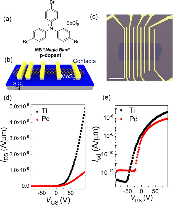
Monolayer (ML) MoS2 flakes were exfoliated onto 300 nm thermally grown SiO2 on a low-resistivity silicon wafer according to the literature-reported gold-mediated exfoliation method from the bulk crystal.17 The number of layers was confirmed by Raman and photoluminescence (PL) spectroscopy (shown in supplementary material Fig. S1). The source/drain contacts were defined by e-beam lithography, followed by electron beam metal deposition and a lift-off process. The deposited source/drain contacts were 30 nm Pd or Ti with 70 nm Au on top to protect from oxidation. As shown in Fig. 1(c), the channel length (L) varies between 1.5 μm and 9 μm. The active area of the channel was patterned using a reactive ion etcher (RIE) by using a gas mixture of SF6 and O2. A bottom-gate top-contact configuration was used with a 300 nm SiO2 dielectric. Figure 1(a) shows the p-dopant, MB, used in this study. MB is a strong p-dopant, and the reduction potential of the functional group [N(C6H4-p-Br)3] + is +0.70 V vs ferrocene.18 During the doping process, the tris(4-bromophenyl)-ammoniumyl radical cation accepts an electron from MoS2 and forms the neutral tris(4-bromophenyl)amine which largely remains in solution and/or is washed away in the following rinsing step. The hexachloroantimonate counterions (SbCl6−) are left on the surface to balance the holes introduced to the film. MB was dissolved in anhydrous dichloromethane (DCM) to make a 5 mmol L−1 solution. The doping treatments were carried out inside a nitrogen glovebox. The devices were immersed in the dopant solutions for various times and were then rinsed with fresh solvent three to five times to remove physisorbed dopants. The electrical characterization of the fabricated devices was collected inside an inert-atmosphere glovebox using a commercial parameter analyzer at room temperature. Unless otherwise noted, electrical parameters reported in the text are the mean and standard deviation.
FIG. 1.
(a) Chemical structures of the p-dopant used in this study. (b) Schematics of a top-contact back-gate monolayer MoS2 transistor with a TLM test structure. (c) Optical image of the MoS2 transistor (scale bar is 25 μm). Representative transfer characteristics of a pristine MoS2 FET at 300 K with either Ti or Pd as the contacts are shown on linear (d) and log (e) scales, VDS = 5 V and L = 5 μm.
Figures 1(d) and 1(e) show the experimental transfer characteristics of typical pristine bottom-gated top-contact ML MoS2 with Ti and Pd metal contacts measured at 300 K. The threshold voltage (VT) is extracted by using the linear extrapolation method with the drain current measured as a function of gate voltage. The VT values for Ti and Pd contacts was found to be (−54 ± 3) V and (−25 ± 4) V, respectively, averaged over tens of devices. The devices exhibit n-FET characteristics regardless of the work function of the metals. The on-current of the high work function metal Pd is smaller than that of the low work function Ti, suggesting that Ti is better aligned with the conduction band of MoS2 and has better electron injection than Pd. These trends are consistent with the previously reported studies of the metal-to-MoS2 interface.19
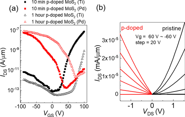
The MoS2 FET devices were first immersed in the 5 mmol L−1 dopant solutions for 10 min. As shown in Fig. 2(a), for both Ti- and Pd-contact FETs, the p-doping treatments shifted the transfer curve to a more positive gate bias after 10 min of treatment [Fig. 2(a), solid square]. An increase in the hole current at negative gate voltage was observed for both contacts to MoS2. Devices with Ti contacts exhibit ambipolar properties with electron transport favored, while Pd contacted MoS2 shows preferred hole transport. The same samples were retreated with an additional 1 h molecular exposure causing VT to shift to more positive back-gate voltage (VGS), consistent with stronger p-doping. However, for the Ti-contact FETs, a decrease is observed in both the electron and hole current and the MoS2 FETs still appear to be ambipolar. For the Pd-contact FETs, large VT shifts (from 40 V to 75 V) and saturation of the ON current at 10−7 A/μm were observed. Significant VT shifts (ΔVT) up to 64 V and 100 V were achieved for Ti- and Pd-contact devices, respectively. The change in hole carrier density (Δp) can be estimated from the Δp = CbgΔVT/q expression, where back-gate capacitance Cbg is estimated from a parallel-plate capacitor model, Cbg = ε0εr/d, with εr = 3.9 for SiO2 and the thickness of the gate dielectric d = 300 nm, and the change of hole sheet density(Δp) is estimated to be 4.6 × 1012cm−2 and 7.2 × 1012cm−2 for Ti- and Pd-contact FETs. Since the MoS2 devices were exposed to the same molecular doping conditions, it is reasonable to assume that the same number of charge carriers was introduced for both Ti- and Pd-contact devices. The smaller change in hole sheet density for the Ti-contacted devices may be attributed to the misalignment of the metal work function and MoS2 valence band, where the doping-induced charge carriers have little impact on the current. The output curves of the pristine n-FET with Pd contacts and doped p-FET are shown in Fig. 2(b). The device performance is summarized in Table I, and the results are the average of 10–15 devices. The pristine Ti-contacted MoS2 shows a higher electron mobility (12.2 ± 1.7 cm2 V−1 s−1) than Pd-contact FETs (8.3 ± 0.9) cm2 V−1 s−1, while 10 min doped Pd-contacted MoS2 devices exhibit a hole mobility of (2.3 ± 0.7) cm2 V−1 s−1. This trend is consistent with a smaller electron injection barrier between Ti-MoS2 favoring electron-transport for both the pristine and doped devices, while in the Pd case, doping has a more dramatic impact, suggesting that the barrier for hole injection is substantially decreased. According to theoretical calculations and experimental results, there are several causes for the Fermi level pinning at the metal contact of MoS2: the van der Waals gap formed at the interface which acts as a tunnel barrier,19 the lack of orbital overlaps between metal and TMDs,20,21 and possible sulfur vacancy defect sites which can act as donors.22 The fact that p-FETs were not observed in Ti-contact devices may be attributed to the lack of orbital overlaps between Ti and p-doped MoS2. For the Pd-contact FETs, the longer treatment time (1 h) decreases the mobility to (0.82 ± 0.12cm2 V−1 s−1). This decrease in the hole mobility is attributed to the increased concentration of ionized scattering centers formed by the doping product, SbCl6− anions. This observation is consistent with previous reports on molecular doping of organic semiconductors23,24 and doping of inorganic semiconductors.25
FIG. 2.
(a) Representative transfer characteristics of a MoS2 FET with Ti and Pd metal contacts after continuously p-doping with MB with two different exposure times. VDS = 5 V and L = 5 μm. (b) Output curves collected from the same Pd-contact device before and after 1 h of MB doping.
TABLE I.
Summary of the comparative transistor performance of ML MoS2 FETs with Ti and Pd contacts before and after the p-doping. Average of ca. 10 samples.31
| Mobility (cm2 V−1 s−1) |
||||||
|---|---|---|---|---|---|---|
| Contacts | Treatment | Electron | Hole | ION/OFF | VT, avg (V) | ΦSB (meV) |
| Ti | Pristine | 12.2 ± 1.7 | ... | 107 | −54 ± 3 | 100a |
| 10 min p-doped | 0.84 ± 0.10 | 6.0 × 10⁻⁵ | 106 | 0 ± 7 | ... | |
| 1 h p-doped | 0.017 ± 0.009 | 9.3 × 10 −6 | 104 | ... | ... | |
| Pd | Pristine | 8.3 ± 0.9 | ... | 106 | −25 ± 4 | 230a |
| 10 min p-doped | 1.4 × 10⁻³ | 2.3 ± 0.7 | 106 | 40 ± 5 | ... | |
| 1 h p-doped | 7.4 × 10⁻⁴ | 0.82 ± 0.12 | 105 | 75 ± 3 | 156b | |
For electron transportation.
For hole transportation.
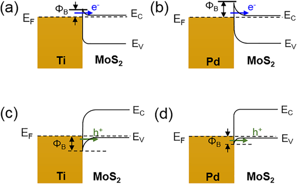
Figure 3 shows qualitative energy band diagrams for MoS2 FETs with Ti and Pd contacts at the metal-MoS2 interface. Both experimental and theoretical results show that the SBH is correlated with the work function of the metal contacts. Lower work function metals (Ti in this case) show improved contacts with pristine MoS2 flakes, as indicated by higher electron injection efficiency and lower contact resistance. Before the molecular doping, the Fermi level of MoS2 is pinned close to the conduction band.22 The interface is strongly impacted by this pinning which occurs close to the conduction band of MoS2, making electron transport dominating. Because of the complicated metal-MoS2 interface, this barrier height cannot be modified effectively by varying the work function of the metal contacts alone.26 The molecular p-dopant molecule interacts with the MoS2 surface via a charge-transfer reaction where electrons are transferred from MoS2 to the p-dopants, making the MoS2 Fermi level shift closer to the valence band edge.27 Thus, doping induces a much higher hole carrier concentration. For the doped low work function Ti-contacted devices, ambipolar behavior was observed with electron transport favored, demonstrating that both high hole concentrations and a low injection barrier are needed for efficient hole transport.
FIG. 3.
Qualitative energy band diagrams for Ti (a) and (c) and Pd (b) and (d) contacted MoS2 FETs in the ON-state showing the SBH height for the electron (a) and (b) and hole (c) and (d) injection at the interface after the p-doping.
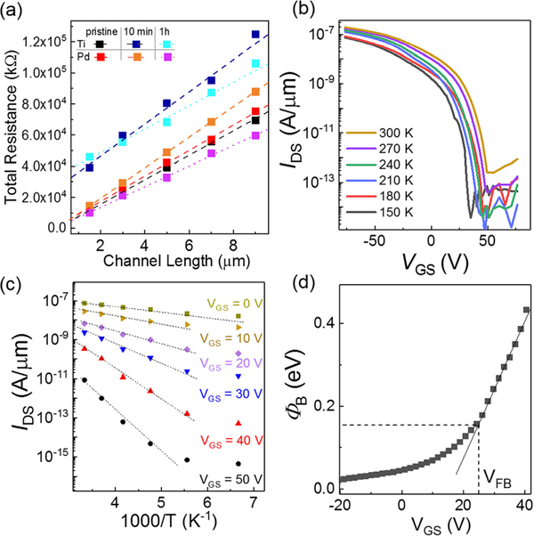
The contact resistance, Rc, before and after doping with different contacts was extracted by using the transfer length method (TLM). The channel width (W) of the lithographically defined MoS2 strip (device channel) is 25 μm. The measured resistance is the aggregate value calculated from the linear I-V characteristics for large voltage sweeps. The VGS is 0 V. Figure 4(a) shows the measured total resistance for different channel lengths. The contact and sheet resistances were extracted from the linear fit of the total resistance, and the contact resistance was normalized for the device width. Before doping, the contact resistances of MoS2 n-FETs were calculated to be (805 ± 65) kΩ μm with Ti contacts and (1430 ± 107) kΩ μm with Pd contacts. These numbers are comparable to previously reported contact resistance for ML MoS2 FETs.28 The Pd contact resistance was reduced to (482 ± 40) kΩ μm after p-doping. Two notable observations are (1) the total resistance increases for the Ti-contact device and decreases for the Pd-contact device after 1 h treatment; (2) contact resistance increases by more than two orders of magnitude for Ti-contact FETs, indicating a larger SBH, and decreases by a factor of three for Pd-contact FETs, indicating improved carrier injection. p-Doping shifts the Fermi level closer to the valence band. Thus, it is expected that higher Rc and higher charge injection barrier are observed with Ti contacts since the work function is closer to the conduction band. In the case of Pd contacts, the work function is closer to the midgap of MoS2, making these devices more sensitive to doping, showing lower Rc and more efficient hole injection. Even though only the channel area was exposed to the dopant treatment, the change in the contact property may be due to the doped one-dimensional edge between the contacts and ML MoS2. It was reported in the literature that graphene with a 1D edge contact can have remarkably low contact resistance.1 It is also possible that the dopants and the injected charge carriers diffuse beneath the metals during immersion in the solution and alter the interfaces. While data such as shown in Fig. S5 suggest such a mechanism, further experimental and theoretical studies are needed to fully understand this effect.
FIG. 4.
Electrical characteristics of p-doped MoS2 devices. (a) The total resistance of MoS2 FETs with different channel lengths. Channel width W = 25 μm. (b) Experimental transfer characteristics of the p-doped MoS2 transistor with Pd contacts at different operating temperatures. The bias voltage is fixed at 5 V, and the channel length is 5 μm. (c) Arrhenius-type plot constructed at different gate voltages. (d) Extracted barrier height as a function of applied gate voltages.
To further evaluate the impacts of doping and different metals on contacts, we also extracted the SBH by using the following equation:
| (1) |
where A is Richardson’s constant, kB is the Boltzmann constant, q is the electronic charge, T is the temperature, ΦB is the effective barrier height, and n is the ideality factor.5 Figures 4(b) and 4(c) show an example of flatband Schottky barrier extraction for the 1 h p-doped MoS2 transistor with Pd contacts. Figure 4(b) shows transfer characteristics at different operating temperatures. These data were used to create the Arrhenius plot in Fig. 4(c). As explained in detail in the literature, thermally assisted tunneling determines the inverse subthreshold slope in Schottky barrier devices.29,30 Figure 4(d) shows that, at sufficiently positive gate voltages, the effective barrier height, ΦB, responds linearly to the gate voltage, VGS, when only thermionic current flows through the device. The flatband voltage, VFB, is reached when tunneling starts to play a role and ΦB deviates from the linear trend mentioned previously. A p-type SBH (ΦSB) of ≈ 156 meV is determined from the Arrhenius plot. The SBH extractions for the pristine MoS2 transistor with Ti and Pd contacts are shown in supplementary material Fig. S2. In the n-type transistor, ΦB responds linearly to VGS at sufficiently negative gate voltages (thermionic regime). The Schottky barrier heights were determined to be ≈ 100 meV and ≈230 meV for Ti- and Pd-contact pristine MoS2 transistors, respectively. A SBH for the p-doped MoS2 transistor with Ti contacts could not be extracted because the tunneling regime was not reached (Fig. S3). A relatively low hole injection barrier can only be obtained for p-doped MoS2 with Pd contacts. The tunneling barrier for holes is too high in Ti-contact devices even after p-doping. These results are consistent with the contact resistance results.
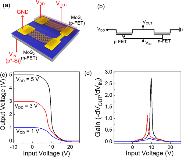
To demonstrate the use of chemical doping for device applications, a complementary inverter was fabricated by wire bonding two Pd-contact MoS2 FETs on the same chip. One of the transistors was immersed in the dopant solution. Figures 5(a) and 5(b) show the device schematic and the electronic circuit. A photograph of the completed device is shown in Fig. S4. The back gate was applied as the input voltage (VIN), and a supply voltage (VDD) was applied to the p-FET. Figure 5(c) shows the voltage transfer characteristics of the inverter at various VDD values. The device operates at a negative input voltage and the switching threshold voltage of the inverter located in the negative region. The slope of the voltage transfer curves in Fig. 5(c) represents the gain of the inverter, which is ≈2.73. Integrating the transistor with a thin high-k dielectric in a top-gate configuration should enhance the voltage gain greatly.
FIG. 5.
(a) Schematic diagram of a MoS2 inverter, (b) The electric circuit of the MoS2 inverter. (c) Voltage-transfer characteristics of the MoS2 inverter at different VDD values. (d) The direct-current voltage gain of the inverter at VDD = 1 V, 3 V, and 5 V. The channels for both n-FET and p-FET are 5 μm.
In 2D-based electronics, the contacts and interfacial properties play important roles in determining device performance. In this work, high-performance p-type field-effect (p-FET) transistors were demonstrated by using chemically doped monolayer MoS2 and high work function metal contacts (Pd). The impact of molecular doping and the metal work function on the charge transport and contact properties of MoS2 devices was presented. Molecular doped p-FETs show an effective hole mobility of 2.3 cm2 V−1 S−1, an on/off ratio exceeding 106, and an improved contact resistance of ≈482 kΩ μm. However, when a low work function metal (Ti) is used to contact MoS2, the device only exhibits ambipolar transport with electron transport favored. It was shown that the SBH can be effectively modulated through doping of the channel materials and the contact engineering by changing the contact metal. A relatively low hole injection barrier of ≈ 156 meV was obtained for p-doped MoS2 with Pd contacts. The utility of MoS2 p- FETs and n-FETs was demonstrated with a complementary inverter. In summary, controlled doping is an important tool for tuning the electronic properties of 2D devices. Both controllable doping and careful contact engineering are important to realize efficient charge injection/extraction and for improving overall device performance. Dopants and contact engineering of TMDs and other emerging materials are powerful tools to fuel the further development of nanoelectronics and optoelectronics.
Supplementary Material
Acknowledgments
S.Z. acknowledges support from the National Institute of Standards and Technology (NIST) Financial Assistance Award with Federal Award ID No. 70NANB16H228. The authors are thankful to Dr. David J. Gundlach and Dr. Emily G. Bittle for their assistance with the electrical measurements.
Footnotes
See the supplementary material for additional results on the optical characterization of MoS2, Schottky barrier extraction, optical image of the MoS2 inverter, and doping results on SiO2 covered transistors.
REFERENCES
- 1.Wang L, Meric I, Huang P, Gao Q, Gao Y, Tran H, Taniguchi T, Watanabe K, Campos L, and Muller D, Science 342(6158), 614–617 (2013). [DOI] [PubMed] [Google Scholar]
- 2.Schulman DS, Arnold AJ, and Das S, Chem. Soc. Rev 47(9), 3037–3058 (2018). [DOI] [PubMed] [Google Scholar]
- 3.Guros NB, Le ST, Zhang S, Sperling BA, Klauda JB, Richter CA, and Balijepalli A, ACS Appl. Mater. Interfaces 11(18), 16683–16692 (2019). [DOI] [PMC free article] [PubMed] [Google Scholar]
- 4.Kang J, Liu W, Sarkar D, Jena D, and Banerjee K, Phys. Rev X 4, 031005 (2014). [Google Scholar]
- 5.Das S, Chen H-Y, Penumatcha AV, and Appenzeller J, Nano Lett. 13(1), 100–105 (2013). [DOI] [PubMed] [Google Scholar]
- 6.Kim G-S, Kim S-H, Park J, Han KH, Kim J, and Yu H-Y, ACS Nano 12(6), 6292–6300 (2018). [DOI] [PubMed] [Google Scholar]
- 7.Laskar MR, Nath DN, Ma L, Lee EW, Lee CH, Kent T, Yang Z, Mishra R, Roldan MA, and Idrobo J-C, Appl. Phys. Lett 104(9), 092104 (2014). [Google Scholar]
- 8.Liu X, Qu D, Ryu J, Ahmed F, Yang Z, Lee D, and Yoo WJ, Adv. Mater. 28(12), 2345–2351 (2016). [DOI] [PubMed] [Google Scholar]
- 9.Nipane A, Karmakar D, Kaushik N, Karande S, and Lodha S, ACS Nano 10(2), 2128–2137 (2016). [DOI] [PubMed] [Google Scholar]
- 10.Neal AT, Pachter R, and Mou S, Appl. Phys. Lett 110(19), 193103 (2017). [Google Scholar]
- 11.Zhang YJ, Ye JT, Yomogida Y, Takenobu T, and Iwasa Y, Nano Lett. 13(7), 3023–3028 (2013). [DOI] [PubMed] [Google Scholar]
- 12.Zhang S, Hill HM, Moudgil K, Richter CA, Walker ARH, Barlow S, Marder SR, Hacker CA, and Pookpanratana SJ, Adv. Mater. 30(36), 1802991 (2018). [DOI] [PMC free article] [PubMed] [Google Scholar]
- 13.Gusev OV, Denisovich LI, Peterleitner MG, Rubezhov AZ, Ustynyuk NA, and Maitlis PM, J. Organomet. Chem. 452(1–2), 219–222 (1993). [Google Scholar]
- 14.Bell F, Ledwith A, and Sherrington D, J. Chem. Soc. C 1969, 2719–2720. [Google Scholar]
- 15.Hajzus JR, Biacchi AJ, Le ST, Richter CA, Walker ARH, and Porter LM, Nanoscale 10(1), 319–327 (2018). [DOI] [PMC free article] [PubMed] [Google Scholar]
- 16.Hölzl J and Schlulze F, Springer Tracts in Modern Physics (Springer-Verlag, 1979). [Google Scholar]
- 17.Desai SB, Madhvapathy SR, Amani M, Kiriya D, Hettick M, Tosun M, Zhou Y, Dubey M, Ager JW, Chrzan D, and Javey A, Adv. Mater 28(21), 4053–4058 (2016). [DOI] [PubMed] [Google Scholar]
- 18.Connelly NG and Geiger WE, Chem. Rev. 96(2), 877–910 (1996). [DOI] [PubMed] [Google Scholar]
- 19.Kim C, Moon I, Lee D, Choi MS, Ahmed F, Nam S, Cho Y, Shin H-J, Park S, and Yoo WJ, ACS Nano 11(2), 1588–1596 (2017). [DOI] [PubMed] [Google Scholar]
- 20.Hu Z, Wu Z, Han C, He J, Ni Z, and Chen W, Chem. Soc. Rev. 47(9), 3100 (2018). [DOI] [PubMed] [Google Scholar]
- 21.Gong C, Colombo L, Wallace RM, and Cho K, Nano Lett. 14(4), 1714–1720 (2014). [DOI] [PubMed] [Google Scholar]
- 22.Liu D, Guo Y, Fang L, and Robertson J, Appl. Phys. Lett. 103(18), 183113 (2013). [Google Scholar]
- 23.Kröger M, Hamwi S, Meyer J, Riedl T, Kowalsky W, and Kahn A, Org. Electron. 10(5), 932–938 (2009). [Google Scholar]
- 24.Olthof S, Mehraeen S, Mohapatra SK, Barlow S, Coropceanu V, Brédas J-L, Marder SR, and Kahn A, Phys. Rev. Lett. 109(17), 176601 (2012). [DOI] [PubMed] [Google Scholar]
- 25.Van Zeghbroeck B, Principles of Electronic Devices (University of Colorado, 2011). [Google Scholar]
- 26.Yang L, Majumdar K, Liu H, Du Y, Wu H, Hatzistergos M, Hung P, Tieckelmann R, Tsai W, and Hobbs C, Nano Lett. 14(11), 6275–6280 (2014). [DOI] [PubMed] [Google Scholar]
- 27.Tarasov A, Zhang S, Tsai M-Y, Campbell PM, Graham S, Barlow S, Marder SR, and Vogel EM, Adv. Mater. 27(7), 1175–1181 (2015). [DOI] [PubMed] [Google Scholar]
- 28.Li S-L, Komatsu K, Nakaharai S, Lin Y-F, Yamamoto M, Duan X, and Tsukagoshi K, ACS Nano 8(12), 12836–12842 (2014). [DOI] [PubMed] [Google Scholar]
- 29.Appenzeller J, Radosavljević M, Knoch J, and Avouris P, Phys. Rev. Lett. 92(4), 048301 (2004). [DOI] [PubMed] [Google Scholar]
- 30.Appenzeller J, Knoch J, Derycke V, Martel R, Wind S, and Avouris P, Phys. Rev. Lett. 89(12), 126801 (2002). [DOI] [PubMed] [Google Scholar]
- 31.The IOn/off and VT values are extracted from the hole side for 10 min and 1 h p-doped MoS2 FETs with Pd contacts.
Associated Data
This section collects any data citations, data availability statements, or supplementary materials included in this article.


