Abstract
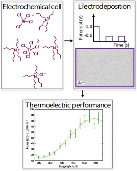
We report the thermoelectric properties of Bi2Te3 thin films electrodeposited from the weakly coordinating solvent dichloromethane (CH2Cl2). It was found that the oxidation of porous films is significant, causing the degradation of its thermoelectric properties. We show that the morphology of the film can be improved drastically by applying a short initial nucleation pulse, which generates a large number of nuclei, and then growing the nuclei by pulsed electrodeposition at a much lower overpotential. This significantly reduces the oxidation of the films as smooth films have a smaller surface-to-volume ratio and are less prone to oxidation. X-ray photoelectron spectroscopy (XPS) shows that those films with Te(O) termination show a complete absence of oxygen below the surface layer. A thin film transfer process was developed using polystyrene as a carrier polymer to transfer the films from the conductive TiN to an insulating layer for thermoelectrical characterization. Temperature-dependent Seebeck measurements revealed a room-temperature coefficient of −51.7 μV/K growing to nearly −100 μV/K at 520 °C. The corresponding power factor reaches a value of 88.2 μW/mK2 at that temperature.
Introduction
There is a growing awareness and concern over the negative effect of greenhouse gasses on the environment, yet fossil fuel combustion still accounts for the majority of energy conversion.1 Moreover, more than 60% of energy worldwide is lost mostly in the form of waste heat.2 Thermoelectric generators could be employed to extract the waste heat and convert it into electricity, thus enabling a better use of existing energy conversion technologies3−5 or possibly thermal sensing.6
Bismuth telluride is the most efficient and most widely used thermoelectric material for low-temperature applications (up to 200 °C).7 Currently, there are a range of fabrication techniques being used for thin film fabrication, such as sputtering, chemical vapor deposition (CVD), pulsed laser deposition (PLD), molecular beam epitaxy (MBE), evaporation, and electrodeposition. In comparison to other methods for thin film fabrication, electrodeposition of such films has advantages of being relatively cost-effective as it does not require high vacuum or elevated temperatures, offers easier control over thickness and composition, and can be used for the deposition of films with thicknesses ranging from nanometers to hundreds of micrometers over a large area. Electrodeposition is also particularly well suited to the deposition on complex geometries.8−10 Electrodeposition of Bi2Te3 thin films has mainly been investigated in aqueous acidic solutions, such as nitric, sulfuric, or hydrochloric acid.11−17 Several electrochemical methods have been employed for electrodeposition of Bi2Te3 thin films, including potentiostatic electrodeposition,11−14,16 galvanostatic electrodeposition,15,17 and pulsed electrodeposition.18−22 Nonaqueous electrolytes have a wider electrochemical window than water, allowing the investigation of more negative overpotentials, and Bi2Te3 thin films have also been successfully electrodeposited from these without the concomitant reduction of the solvent. Organic solvents also provide improved solubility of Bi(III) and Te(IV) salts, which are only moderately soluble in aqueous acidic media limiting the deposition rate. The use of nonaqueous solvents also widens the range of precursor salts that can be employed compared with that of aqueous media. The electrodeposition of Bi2Te3 thin films from nonaqueous solvents, such as dimethyl sulfoxide (DMSO),22 ethylene glycol,23 chloride-free ethylene glycol,24 and a 1-ethyl-1-octyl-piperidinium TFSI/1-ethyl-1-octyl-piperidinium bromide mixture25 have been reported in the literature.
We recently reported the potentiostatic electrodeposition of Bi2Te3 thin films from dichloromethane.26 Although we were successful in controlling the composition of these films by varying the deposition potential, the films were highly porous and made up of small crystallites. In this work, we show that using nucleation pulses and pulsed electrodeposition allows significant improvement of the film morphology and consequently the thermoelectric properties. In addition, a thin film transfer process was successfully developed allowing thermoelectric characterization of these films for the first time. The films were transferred from the TiN electrodes onto an insulating substrate (SiO2) for subsequent electrical characterization using polystyrene as a carrier polymer. Unlike commonly used poly(methyl methacrylate),27 polystyrene has advantages of easier removal after the transfer and does not form wrinkles on the transferred films resulting in a complete transfer of the deposited film.28 Electrodeposited bismuth telluride thin films reported in the literature have so far been transferred by epoxy resin for thermoelectric measurements.29−31 However, the epoxy method leaves cracks in the transferred films visible through a microscopy and the delamination from the original substrate is not complete. Here, we show that electrodeposited bismuth telluride thin films can be completely lifted from its original substrate and transferred to an insulating substrate without cracks visible by the optical microscope nor electron microscopy.
Results and Discussion
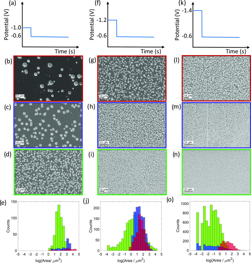
To improve the film morphology of the Bi2Te3 films electrodeposited using potentiostatic conditions in our previous work,26 nucleation of the film has been optimized. The Bi2Te3 films were grown by introducing a short initial nucleation pulse at a high overpotential, which generates a large number of nuclei, and then growing them potentiostatically or by pulsed deposition at lower overpotential. First, the early stage of film growth was investigated by applying a short nucleation pulse at high overpotentials, after which the nuclei were grown potentiostatically at −0.6 V vs Ag/AgCl with a passed charge of −0.26 C, which would correspond to 200 nm thickness assuming a uniform distribution over the whole electrode area (Supporting Information, Section S3). Figure 1 shows a schematic, scanning electron microscopy (SEM) images, and histograms of the size distribution of the resulting deposited particles. The deposits were grown by applying an initial nucleation pulse of −1.0, −1.2, and −1.4 vs Ag/AgCl for 1, 3, or 5 s. As can be seen from the figure, by increasing the length of the nucleation pulse, an increased coverage of the substrate surface was achieved with smaller and more uniform particles. In addition, by applying a higher initial overpotential for the same amount of time, the same effect of generating smaller, denser, and more uniform nuclei was achieved. This indicates progressive nucleation, meaning that the nucleation process is slow and new nuclei continue to form during the deposition, while those already formed continue to grow. Hence, by applying a potential of −1.4 V for 5 s and then growing the nuclei at −0.6 V vs Ag/AgCl, almost full coverage of uniform, densely packed particles was obtained. ImageJ32 was used to extract the number and the areal size of the electrodeposited crystallites plotted as histograms. The deposits formed with nucleation potentials of −1.0 V for 5 s and −1.4 V for 5 s show particle counts of at least a factor of 10 higher than the deposits formed with shorter pulses at lower potential. This corresponds to a volume particle size reduction of the same factor. These nucleation pulse values were therefore selected for further investigation and optimization of bismuth telluride thin film growth.
Figure 1.
SEM images and histograms of electrodeposited bismuth telluride deposits grown at Edep = −0.6 V, preceded by nucleation pulses of Enuc = −1.0 V (a–e), −1.2 V (f–j), and −1.4 V vs Ag/AgCl (k–o), with nucleation pulse times tnuc = 1 s (red: b, g, l), 3 s (blue: c, h, m), and 5 s (green d, i, n).
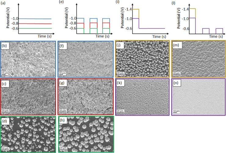
Figure 2 shows SEM images of films grown potentiostatically (Figure 2b–d), by pulsed electrodeposition (Figure 2f–h), potentiostatically preceded by a nucleation pulse (Figure 2j,k), and by pulsed deposition preceded by a nucleation pulse (Figure 2m,n). Growing films by pulsed electrodeposition yields somewhat smoother films with improved composition repeatability compared to those grown potentiostatically. For the pulsed deposition during the off-time, when no current passes, the concentrations of Bi and Te species at the electrode surface replenish by diffusion. As a result, under pulsed conditions, the composition of the films can be better controlled due to the replenishment of the reactants in each cycle.19 The duration of on- and off-pulses during pulsed electrodeposition was optimized to 5 s on-time and 10 s off-time. As can be seen from Figure 2, both the films grown potentiostatically and by pulsed electrodeposition at potentials of −1.0 V (Figure 2b,f) and −0.8 V (Figure 2c,g) vs Ag/AgCl exhibit similar porous but continuous morphologies. The thickness of the films is estimated to be 1 μm from the total charge passed of −1.3 C for potentiostatically grown films. For the films grown by pulsed deposition, the estimated thickness is 950 nm from the charge passed of −1.2 C and 1.4 μm from the charge passed of −1.8 C for films grown at −1.0 and −0.8 V vs Ag/AgCl, respectively. However, when growing films potentiostatically and by pulsed electrodeposition at a lower potential of −0.6 V vs Ag/AgCl, a significant change in morphology was observed (Figure 2d,h). The resulting deposits in this case are not films but rather comprise discontinuous islands. Furthermore, the deposits obtained by pulsed electrodeposition are smoother, slightly larger, and more uniform in size than the deposits obtained potentiostatically. The calculated thickness of the uniform film over the given area grown potentiostatically is 1, and 1.8 μm from a charge of −2.3 C for the film grown by pulsed deposition at −0.6 V vs Ag/AgCl. Table 1 gives the average and standard deviation of Bi-to-Te ratios and atomic percentage of oxygen measured by energy-dispersive X-ray (EDX) elemental analysis on three different areas of the films. The presence of Bi and Te confirms the deposition of bismuth telluride, with slight variation of the average Bi-to-Te ratios from stoichiometric composition (0.7) when applying different potentials and deposition methods. Furthermore, the small standard deviation (≤0.05) in Bi-to-Te ratios obtained in all films proves excellent composition uniformity regardless of the method. The O signal most probably indicates oxidation of the bismuth telluride films.
Figure 2.
Schematics and SEM images of potentiostatic (a–d), pulsed (e–h), potentiostatic preceded by nucleation pulse (i–k), and pulsed preceded by nucleation pulse (l–n); bismuth telluride deposition for potentials of −1.0 V (b, f), −0.8 V (c, g), −0.6 V (d, h), and −0.6 V preceded by nucleation pulses of −1.4 V (j, m) and −1.0 V (k, n) vs Ag/AgCl. ton = 5 s and toff = 10 s for all pulsed electrodepositions.
Table 1. Elemental Composition Showing Bi-to-Te Atomic Ratios and Atomic Percentage of O Measured on Three Different Areas of the Film Showing Average Values and Standard Deviationa.
| method | potential vs Ag/AgCl/V | Bi:Te ± stdev | % atomic O ± stdev |
|---|---|---|---|
| potentiostatic | Edep = −1.0 | 0.5 ± 0.01 | 32.4 ± 1.08 |
| potentiostatic | Edep = −0.8 | 0.5 ± 0.01 | 38.0 ± 0.25 |
| potentiostatic | Edep = −0.6 | 0.8 ± 0.03 | 13.1 ± 0.46 |
| pulsed | Edep = −1.0 | 0.7 ± 0.03 | 33.8 ± 1.83 |
| pulsed | Edep = −0.8 | 0.6 ± 0.02 | 17.8 ± 4.41 |
| pulsed | Edep = −0.6 | 0.8 ± 0.05 | 13.8 ± 3.73 |
| potentiostatic with nucleation pulse | Edep = −0.6, Enuc = −1.4 | 0.6 ± 0.04 | 4.4 ± 0.26 |
| potentiostatic with nucleation pulse | Edep = −0.6, Enuc = −1.0 | 0.9 ± 0.01 | 26.0 ± 1.44 |
| pulsed with nucleation pulse | Edep = −0.6, Enuc = −1.4 | 0.5 ± 0.02 | 0.3 ± 0.50 |
| pulsed with nucleation pulse | Edep = −0.6, Enuc = −1.0 | 0.7 ± 0.01 | 6.5 ± 0.95 |
All films are electrodeposited from an electrolyte containing 2.25 mM [NnBu4][BiCl4], 3 mM [NnBu4]2[TeCl6], and 0.1 M [NnBu4]Cl by different methods. ton = 5 s and toff = 10 s for all pulsed depositions.
The films grown potentiostatically and by pulsed electrodeposition preceded by a nucleation pulse are compared. As can be seen in Figure 2, considerable change in morphology is noticeable between films grown potentiostatically (Figure 2j,k) and by pulsed electrodeposition (Figure 2m,n) after introducing an initial nucleation pulse at higher potential. The films grown by pulsed electrodeposition are compact, continuous, and smooth, while those grown potentiostatically are discontinuous. The calculated thickness of the deposits electrodeposited potentiostatically is 1 μm. For the films grown by pulsed electrodeposition, the calculated thickness from the passed charge of −0.6 C is 500 nm and 1.4 μm for a charge of −1.8 C for nucleation potentials of −1.0 and −1.4 V vs Ag/AgCl, respectively. Cross-sectional SEM images of the films electrodeposited by pulsed electrodeposition preceded by a nucleation pulse reveal the actual thicknesses of 675 nm and 2 μm for nucleation pulses of −1.0 and −1.4 V vs Ag/AgCl, respectively. The 35% discrepancy between the calculated and measured values is possibly due to the residual porosity in the films. On the other hand, the calculated thickness of the porous film electrodeposited potentiostatically at −1 V vs Ag/AgCl is 1 μm, while the cross-sectional SEM reveals a thickness of 4.5 μm. This large factor of 4 discrepancy between the theoretical and measured values is definitely due to the porosity of the film. Furthermore, as shown in Table 2, the oxygen content is significantly lower in films grown by pulsed deposition preceded by a nucleation pulse compared to that of films obtained by other methods. This is probably due to the compact and smooth surface morphology of these films that have a smaller exposed surface area than that of the porous films and are therefore less prone to atmospheric oxidation.
Table 2. Lattice Parameters and Crystallite Sizes for Different Bismuth Telluride Films from X-ray Diffraction Data Obtained Using the PDXL Programme.
| method | potential | a (Å) | c (Å) | crystallite size (Å) |
|---|---|---|---|---|
| potentiostatic | Edep = −1.0 V | 4.16(10) | 30(3) | 18 |
| pulsed | Edep = −1.0 V | 4.1(4) | 30.0(19) | 27 |
| pulsed | Edep = −0.6 V | 4.48(6) | 28.8(5) | 35 |
| pulsed with an initial nucleation pulse | Edep = −0.6 V, Enuc = −1.0 V | 4.35(8) | 29.2(5) | 41 |
| pulsed with an initial nucleation pulse | Edep = −0.6 V, Enuc = −1.4 V | 4.33(4) | 30.0(5) | 36 |
Crystal Structure of Electrodeposited Bismuth Telluride Films
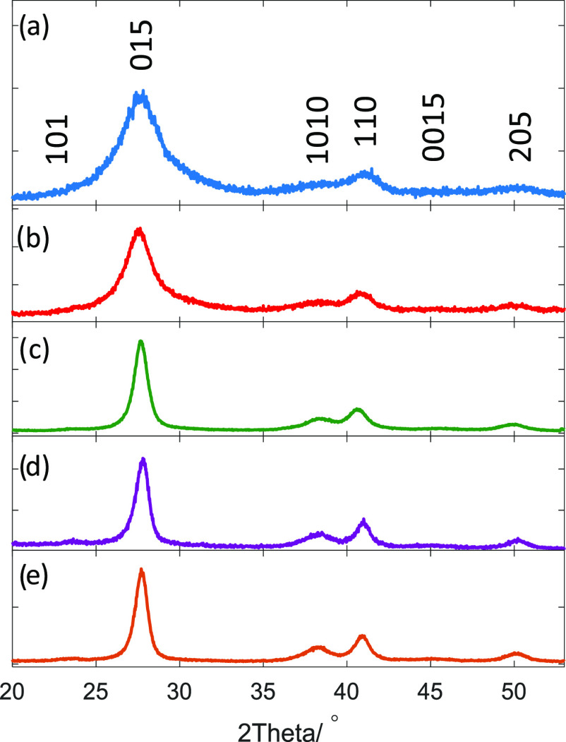
Figure 3 shows the
diffraction patterns of bismuth telluride films electrodeposited onto
TiN electrodes; there are peaks at 2θ angles of 23.64, 27.71,
38.31, 40.97, 45.10, and 50.05°. The X-ray diffraction analysis
of bismuth telluride thin films electrodeposited by different methods
shows that the diffraction patterns are very similar regardless of
the method. The peaks can be attributed to trigonal Bi2Te3, although the presence of elemental Te cannot be completely
discounted as they share many reflection positions. The results were
fitted against the literature pattern33 and show good agreement. The 015 reflection at 27.7° is of
the highest intensity for all of the films, and its width indicates
crystallite size with the broadest indicating the smallest and the
narrowest indicating the largest crystallite size. This relationship
between the peak width and the crystallite size is given by the Scherrer
equation 
Figure 3.
X-ray diffraction (XRD) patterns collected on bismuth telluride films electrodeposited potentiostatically at −1.0 V (a), by pulsed deposition at −1.0 V (b), by pulsed deposition at −0.6 V without an initial nucleation pulse (c), and by pulsed deposition at −0.6 V with an initial nucleation pulse at −1.0 V (d) and −1.4 V (e) vs Ag/AgCl. ton = 5 s and toff = 10 s for all pulsed depositions.
Crystallite sizes of bismuth telluride films electrodeposited by different methods were obtained using the PDXL package and are shown in Table 2. The smallest crystallite size was obtained for films electrodeposited potentiostatically at −1 V vs Ag/AgCl, which corresponds to the highest nucleation rate. The films obtained by pulsed electrodeposition at the same potential exhibit larger crystallite size. Growing films at an even lower overpotential of −0.6 V vs Ag/AgCl by pulsed electrodeposition gave a much larger crystallite size due to the lower nucleation rate at the lower overpotential. The films electrodeposited by pulsed electrodeposition at a lower overpotential of −0.6 V vs Ag/AgCl preceded by a nucleation pulse also possess a larger crystallite size, comparable to those grown without a nucleation pulse. Thus, it is possible to alter the crystallite sizes of bismuth telluride films, which, in turn, could have a beneficial effect on the electrical conductivity and therefore the thermoelectric properties of the films.
Oxidation of Bismuth Telluride Films
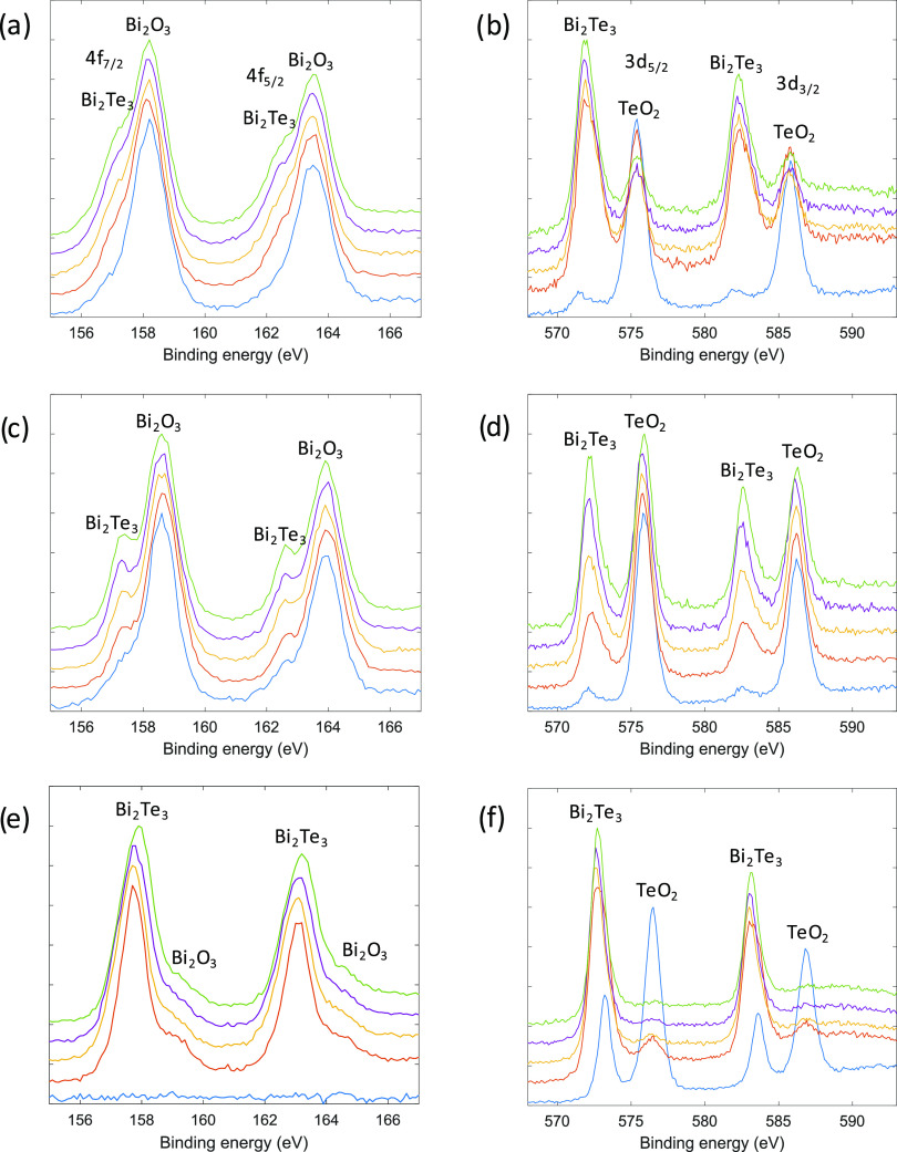
Surface oxidation of electrodeposited bismuth telluride films was investigated by X-ray photoelectron spectroscopy (XPS). XPS measurements were carried out on films electrodeposited by pulsed electrodeposition either with or without an initial nucleation pulse, as shown in Figure 4. The samples were taken out of the solution after the deposition and transferred onto an insulating substrate within a couple of days before the measurements were taken. The scans show the Bi 4f and Te 3d doublets. For each sample, the first measurement was taken at the surface layer followed by four cycles of etching with Ar ions for 60 s to expose deeper layers in the bulk of the material. The etching rate is approximately 0.5 nm/s, meaning that after each etching cycle measurements were taken 30 nm deeper in the bulk of the material. The reference for XPS spectra analysis is the C 1s peak at a binding energy of 284.8 eV. The Bi 4f7/2 peak is composed of two contributions at 157.4 ± 0.3 and 158.6 ± 0.4 eV corresponding to Bi in Bi2Te3 and Bi in Bi2O3, respectively, with the associated Bi 4f5/2 peaks at 162.8 ± 0.3 and 163.9 ± 0.5 eV.34−37 The two peaks for Bi–Te and Bi–O are observed due to spin–orbital splitting of the f-orbital into f5/2 and f7/2 components with an area ratio of 3/4. In our cases, the free fitted area ratio is 0.79 for both Bi–Te and Bi–O. The Te has contributions of 3d5/2 at 572.1 ± 0.4 and 575.8 ± 0.5 eV corresponding to Bi2Te3 and TeO2, respectively. The contributions of 3d3/2 are at 582.6 ± 0.4 eV and 586.2 ± 0.5 eV.34−37 The free fitted area ratio of the d5/2 and d3/2 doublets is 0.69, close to a theoretical value of 2/3.
Figure 4.
Bi 4f (left) and Te 3d (right) regions of the XPS spectra for bismuth telluride films electrodeposited: by pulsed electrodeposition at −1.0 V (a, b), pulsed electrodeposition at −0.6 V preceded by a nucleation pulse at −1.0 V (c, d), and a nucleation pulse at −1.4 V (e, f). Blue: surface prior to etching, orange: after 60 s of etching, yellow: after 120 s of etching, purple: after 180 s of etching, and green: after 240 s of etching.
The Bi peaks in films electrodeposited by pulsed electrodeposition show that the Bi2O3 peaks have higher intensities than Bi2Te3 even in deeper layers of the material, although the Bi2Te3 peak intensities increase slightly as deeper layers are exposed (Figure 4a). The more compact and smoother film electrodeposited by pulsed electrodeposition with an initial nucleation pulse at −1.0 V shows a similar trend (Figure 4c). For both films, the Te on the surface is mainly in the form of TeO2, while after exposure of the deeper layers Te in the form of Bi2Te3 is more prominent although a significant contribution from TeO2 is still present (Figure 4b,d).
In contrast, in the case of the film electrodeposited with an initial nucleation pulse at −1.4 V, there is no Bi at all in the surface layer, and the deeper layers are composed of Bi2Te3 with an almost negligible amounts of Bi2O3 (Figure 4e). The Te spectra confirm the Bi spectral observation for this film. Here, the surface layer is predominantly Te in the form of TeO2 with a significant amount of Bi2Te3, and the deeper layers are in the form of Bi2Te3 with a negligible amount of oxidized Te (Figure 4f). The film possesses Te termination, which is mainly oxidized and prevents further oxidation of the underlying film. These data are in full agreement with the EDX data, which showed 33.8 and 6.5% of oxygen for the former two films, and 0.3% for the film with the initial nucleation pulse at −1.4 V followed by the pulsed electrodeposition at −0.6 V. Music et al.38 also observed that Te termination of bismuth telluride slows down the oxidation of Bi2Te3. After the last etching cycle, the measurements were taken about 120 nm into the bulk of the material, still revealing at least some oxidation in the bulk as a result of oxygen diffusion. Although it was reported that Bi2Te3 thin films grown by molecular beam epitaxy are stable and surface oxidation occurs on the time scale of months,39 in the case of porous films the oxidation is significant and can be reduced by decreasing the surface-to-volume ratio and, more importantly, by obtaining Te termination on the surface.
Thin Film Transfer
The separation of the bismuth telluride film was achieved in KOH solution, as KOH acts on the interface between the substrate and lifting the film. The separation then gradually spreads due to capillary wetting. Figure 6a,b shows images taken under the optical microscope of a bismuth telluride film electrodeposited onto a TiN electrode and a bismuth telluride film transferred to the SiO2 substrate, respectively. Although polystyrene residues are visible on the film after the transfer, the transfer process is complete and the transferred films are uniform without wrinkles or cracks (Figure 6b). Figure 6c,d shows SEM images of the bismuth telluride film before and after transfer; they also show that there are no cracks in the film after transfer, demonstrating the integrity of the transfer process.
Figure 6.
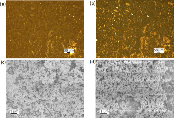
Optical images of a bismuth telluride film electrodeposited on a TiN electrode (a) before the transfer and (b) after transfer to the SiO2 substrate. SEM images of a bismuth telluride film (c) before and (d) after the transfer.
Thermoelectric Characterization
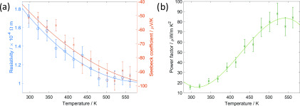
Thermoelectric characterization was conducted on the film electrodeposited by pulsed electrodeposition at −0.6 V vs Ag/AgCl for on-time 5 s and off-time 10 s with an initial nucleation pulse of −1.0 V vs Ag/AgCl for 5 s. The electrodeposited film is n-type with a charge carrier concentration of (2.8 ± 1.2) × 1020 cm–3 and a resistivity of 15.9 mΩ cm at room temperature obtained from Hall measurements. The resistivity decreases with increasing temperature (Figure 7a), meaning that the electrodeposited bismuth telluride film exhibits semiconducting behavior with further thermal activation at higher temperature. The film exhibits a Seebeck coefficient of −51.7 μV/K at 300 K, which increases with temperature reaching a value of −96.6 μV/K at 520 K (Figure 7a). The decrease in Seebeck coefficient after 520 K is due to the bipolar effect. At the temperature of ∼500 K, electrons from the valence band are elevated into the conduction band. This gives rise to minority carriers (in this case, holes), traveling in the opposite direction. The two types of carriers have opposite signs of Seebeck coefficient canceling each other and therefore decreasing the material’s Seebeck coefficient with further temperature increase. The power factor is defined as S2σ, meaning that it depends only on the Seebeck coefficient and the electrical conductivity of the material. Figure 7b shows the power factor of the thin film as a function of temperature, showing that the power factor increases with increasing temperature reaching a value of 88.2 μW/mK2 at 520 K, in accordance with the increase in Seebeck coefficient. The porous films obtained potentiostatically or by pulsed electrodeposition are insulating probably due to oxidation of the films as a result of high surface-to-volume ratio, and no Seebeck or resistivity data could be extracted. There is a range of values for Seebeck coefficient and resistivity of electrodeposited bismuth telluride thin films reported in the literature. However, we compare our data to that from the Martin-Gonzalez group19,21,40 who carried out an extensive study on electrodeposition of bismuth telluride thin films from an aqueous solution. The obtained carrier concentration and the Seebeck coefficient values of our electrodeposited bismuth telluride films are close to the reported data; however, the resistivity value is higher than the reported ones. Manzano et al.21 reported a carrier concentration of 3.2 × 1020 cm–3 and a Seebeck coefficient of −58 μV/K, which correspond to our measured values of (2.8 ± 1.2) × 1020 cm–3 for carrier concentration and −51.7 μV/K for Seebeck coefficient. The reported resistivity is 1.5 mΩ cm, lower than our measured value of 15.9 mΩ cm.
Figure 7.
Dependence of (a) resistivity and Seebeck coefficient, and (b) power factor with temperature for the bismuth telluride film electrodeposited by pulsed electrodeposition at −0.6 V vs Ag/AgCl for on-time 5 s and off-time 10 s with an initial nucleation pulse to −1 V vs Ag/AgCl for 5 s. Error bars are based on the tool manufacturer’s information. Lines are guides to the eye.
Conclusions
Bismuth telluride films were fabricated by potentiostatic and pulsed electrodeposition with or without a preceding nucleation pulse from dichloromethane, using [NnBu4][BiCl4] and [NnBu4]2[TeCl6] as the Bi and Te precursors. The composition repeatability between replicate samples was significantly improved in films produced by pulsed electrodeposition compared to those obtained potentiostatically. In addition, somewhat smoother films were obtained by pulsed electrodeposition; however, both methods yield either porous or discontinuous films, which are unsuitable for thermoelectric applications. Nucleation of the films was optimized by applying an initial nucleation pulse at high overpotential followed by growth of the films either potentiostatically or by pulsed electrodeposition at lower overpotential. The films grown potentiostatically preceded by a nucleation pulse are discontinuous, while those grown by pulsed electrodeposition preceded by a nucleation pulse are continuous, compact, and smooth. XPS measurements reveal that the porous films are prone to oxidation, possibly due to their high surface-to-volume ratio, while the smooth and compact films are significantly less oxidized. Moreover, it was found that if the smooth and compact films were Te-terminated the oxidation was suppressed. The effect of oxidation was also observed in EDX compositional analysis, where the oxygen content dropped considerably for smooth films obtained by pulsed electrodeposition preceded by a nucleation pulse as compared to that of the porous films. The XRD measurements show that films grown at a lower overpotential have larger crystallite sizes, and the films grown at a lower overpotential either with or without a preceding nucleation pulse exhibit similar crystallite sizes. To perform electrical measurements, the films were transferred using polystyrene as a carrier polymer. The transfer process was complete, and the films had no wrinkles or cracks after transfer. The porous films produced by potentiostatic and pulsed electrodeposition were found to be insulating most probably due to their high surface area prone to oxidation, which degrades the thermoelectric properties of these films. The compact and smooth film produced by pulsed electrodeposition at −0.6 V preceded by a nucleation pulse at −1.0 V vs Ag/AgCl exhibits semiconducting behavior with the resistivity of the film decreasing with increasing temperature. The temperature-dependent Seebeck coefficient measurements show a Seebeck coefficient of −51.7 μV/K at room temperature, reaching −96.6 μV/K at 520 K. The power factor reaches a value of 88.2 μW/mK2 at 520 K.
Materials and Methods
Electrodeposition
Electrolytes were prepared in anhydrous CH2Cl2 (Sigma-Aldrich, 95%) and dried by refluxing with CaH2 (followed by distillation and then stored in the glovebox; the water content in the dried CH2Cl2 was ca. 18 ppm) with the addition of 0.1 M [NnBu4]Cl (Sigma-Aldrich, ≥99.0%, as-received) as the supporting electrolyte. The Bi and Te precursors ([NnBu4][BiCl4] and [NnBu4]2[TeCl6]) were synthesized as described in the literature.41
The cyclic voltammetry (Supporting Information, Section S1) and electrodeposition experiments were carried out in a recirculating glovebox (Belle Technology, U.K.) using an Autolab potentiostat (μAUT70706). The experiments were carried out in an electrolyte containing 2.25 mM [NnBu4][BiCl4], 3 mM [NnBu4]2[TeCl6], and 0.1 M [NnBu4]Cl in anhydrous CH2Cl2 using a three-electrode system with a 1 cm diameter Pt coin as the counter electrode, and an Ag/AgCl (0.1 M [NnBu4]Cl in anhydrous CH2Cl2) as the reference electrode. As the working electrode, either a 3 mm diameter glass-sealed glassy carbon (GC, Sigradur G, HTW, Germany) or 7 × 11 mm titanium nitride (TiN) electrode was used. The glass-sealed GC electrode was used for precursor characterization experiments. It was cleaned by polishing with alumina powder (1 μm and 0.05 μm diameters in sequence, micropolish, Buehler, Germany) on a water-saturated polishing pad (Microcloth, Buehler). The fabrication of 7 × 11 mm TiN working electrodes is described in our previous work.41
Thin Film Characterization
Scanning electron microscopy (SEM) was performed using a Zeiss EVO LS 25 with an accelerating voltage of 10 kV, and energy-dispersive X-ray (EDX) data were obtained with an Oxford INCAx-act X-ray detector. EDX calibration was carried out using a Bi2Te3 powder standard (Strem Chemicals, 99.99%). High-resolution SEM measurements were carried out with a field emission SEM (Jeol JSM 7500F) at an accelerating voltage of 2 kV. X-ray diffraction (XRD) measurements were carried out using a Rigaku Smartlab diffractometer either in symmetric or in grazing incidence mode (θ1 = 1°) with a 9 kW Cu Kα (λ = 1.5418 Å) source, a parallel line focus incident beam, and a Hypix detector. Phase matching and lattice parameter refinement were carried out using the PDXL2 software package and diffraction patterns from the Inorganic Crystal Structure Database (ICSD).33 X-ray photoelectron spectroscopy (XPS) data were obtained using a ThermoScientific Theta Probe System with Al–Kα radiation (photon energy = 1486.6 eV). XPS depth profiling was performed by using an Ar ion gun at a beam voltage of 3 kV on a 2 × 2 mm raster area.
The in-plane electrical conductivity (σ) and Seebeck coefficient (S) were simultaneously measured on a commercial JouleYacht Thin-film Thermoelectric Parameter Test System (MRS-3L). The system was calibrated using a nickel foil reference standard, and the measurement accuracy was found to be within 5% for resistivity and 7% for Seebeck coefficient measurements. The Hall coefficient (RH) was determined at 300 K on a Nanometrics HL5500PC instrument using a van de Pauw configuration. The carrier concentration (n) and in-plane mobility (μ) were calculated according to 1/n = eR and μ = σR, respectively.
Thin Film Transfer
Target substrates of 1 × 1 cm with 50 nm thick SiO2 were fabricated by dry thermal oxidation of a Si wafer in a Tempress Furnace tube. Twenty grams of polystyrene (Sigma-Aldrich, Mw ∼ 280 000 by GPC) was dissolved in 100 mL of toluene (Fisher Chemical) to prepare 20 w/v% solution. The solution was spin-coated on the Bi2Te3 thin films at 500 rpm for 10 s followed by 1000 rpm for 50 s. The samples were then baked at 85 °C for 30 min to dry the polymer. A cut was made on the samples to allow solution to penetrate between the Bi2Te3 films coated with PS and the TiN substrates. The samples were then dipped into an AZ 400K (Merck, 2% KOH) solution, which enables exfoliation of the Bi2Te3 films. Afterward, the films coated with the polymer were transferred onto SiO2 substrates and left to dry in air for 3 days to allow adhesion of the bismuth telluride films to the SiO2 substrates. Prior to the film transfer, the SiO2 substrates were activated by O2 plasma for 5 min in a Plasmalab 80 Plus (RIE) to improve adhesion of the transferred films. Finally, the carrier polymer was dissolved from Bi2Te3 films by dipping the samples in chloroform (Sigma-Aldrich, ≥99%). The films were then dipped into acetone and isopropanol to remove the solvent (a schematic diagram of the transfer process can be found in Figure 5).
Figure 5.
Schematic of the polystyrene-based process used to transfer Bi2Te3 films electrodeposited on TiN to an insulating SiO2 substrate.
Optical microscopy (Nikon Eclipse LV150) and high-resolution SEM (field emission SEM, Jeol JSM 7500F; an accelerating voltage of 2 kV) were used to characterize the films before and after the transfer.
Acknowledgments
This work is part of the ADEPT (Advanced Devices by ElectroPlaTing) project funded by a Programme grant from the EPSRC (EP/N035437/1). The authors thank EPSRC for funding the Smartlab diffractometer under EP/K00509X/1 and EP/K009877/1. The authors also thank Dr. Jamie D. Reynolds for helpful advices about film transfer process. All data supporting this study are openly available from the University of Southampton repository at DOI: https://doi.org/10.5258/SOTON/D1367.
Supporting Information Available
The Supporting Information is available free of charge at https://pubs.acs.org/doi/10.1021/acsomega.0c01284.
Cyclic voltammetry in an electrolyte containing 2.25 mM [NnBu4][BiCl4] and 3 mM [NnBu4]2[TeCl6] (Section S1), image of a substrate with the electrodeposited bismuth telluride film (Section S2), and film thickness calculation (Section S3) (PDF)
The authors declare no competing financial interest.
Supplementary Material
References
- International Energy Outlook 2016, www.eia.gov/forecasts/ieo/pdf/0484(2016).pdf, May 2016.
- Zhang X.; Zhao L.-D. Thermoelectric Materials: Energy Conversion between Heat and Electricity. J. Mater. 2015, 1, 92–105. 10.1016/j.jmat.2015.01.001. [DOI] [Google Scholar]
- Bell L. E. Cooling, Heating, Generating Power, and Recovering Waste Heat with Thermoelectric Systems. Science. 2008, 321, 1457–1461. 10.1126/science.1158899. [DOI] [PubMed] [Google Scholar]
- Tritt T. M. Thermoelectric Phenomena, Materials, and Applications. Annu. Rev. Mater. Res. 2011, 41, 433–448. 10.1146/annurev-matsci-062910-100453. [DOI] [Google Scholar]
- LeBlanc S. Thermoelectric Generators: Linking Material Properties and Systems Engineering for Waste Heat Recovery Applications. Sustainable Mater. Technol. 2014, 1, 26–35. 10.1016/j.susmat.2014.11.002. [DOI] [Google Scholar]
- Chen J.; Hu H.; Wang J.; Liu C.; Liu X.; Li Z.; Chen N. A d-Band Electron Correlated Thermoelectric Thermistor Established in Metastable Perovskite Family of Rare-Earth Nickelates. ACS Appl. Mater. Interfaces 2019, 11, 34128–34134. 10.1021/acsami.9b12609. [DOI] [PubMed] [Google Scholar]
- Witting I. T.; Chasapis T. C.; Ricci F.; Peters M.; Heinz N. A.; Hautier G.; Snyder G. J. The Thermoelectric Properties of Bismuth Telluride. Adv. Electron. Mater. 2019, 5, 201800904 10.1002/aelm.201800904. [DOI] [Google Scholar]
- Burton M. R.; Richardson S. J.; Staniec P. A.; Terrill N. J.; Elliott J. M.; Squires A. M.; White N. M.; Nandhakumar I. S. A Novel Route to Nanostructured Bismuth Telluride Films by Electrodeposition. Electrochem. Commun. 2017, 76, 71–74. 10.1016/j.elecom.2017.02.004. [DOI] [Google Scholar]
- Li X.; Koukharenko E.; Nandhakumar I. S.; Tudor J.; Beeby S. P.; White N. M. High Density p-Type Bi0.5Sb1.5Te3 Nanowires by Electrochemical Templating through Ion-Track Lithography. Phys. Chem. Chem. Phys. 2009, 11, 3584–3590. 10.1039/b818040g. [DOI] [PubMed] [Google Scholar]
- Martín J.; Manzano C. V.; Caballero-Calero O.; Martin-Gonzalez M. High-Aspect-Ratio and Highly Ordered 15-nm Porous Alumina Templates. ACS Appl. Mater. Interfaces 2013, 5, 72–79. 10.1021/am3020718. [DOI] [PubMed] [Google Scholar]
- Yoo I. J.; Myung N. V.; Lim D. C.; Song Y.; Jeong Y. K.; Kim Y.; Do; Lee K. H.; Lim J. H. Electrodeposition of BixTey Thin Films for Thermoelectric Application. Thin Solid Films 2013, 546, 48–52. 10.1016/j.tsf.2013.05.036. [DOI] [Google Scholar]
- Heo P.; Hagiwara K.; Ichino R.; Okido M. Electrodeposition and Thermoelectric Characterization of Bi2Te3. J. Electrochem. Soc. 2006, 153, C213. 10.1149/1.2168378. [DOI] [Google Scholar]
- Kang W. S.; Li W. J.; Chou W. C.; Tseng M. F.; Lin C. S. Microstructure and Thermoelectric Properties of Bi2Te3 Electrodeposits Plated in Nitric and Hydrochloric Acid Baths. Thin Solid Films 2017, 623, 90–97. 10.1016/j.tsf.2016.12.047. [DOI] [Google Scholar]
- Jiang Q.; Liu C.; Song H.; Xu J.; Mo D.; Shi H.; Wang Z.; Jiang F.; Lu B.; Zhu Z. Free-Standing PEDOT: PSS Film as Electrode for the Electrodeposition of Bismuth Telluride and Its Thermoelectric Performance. Int. J. Electrochem. Sci. 2014, 9, 7540–7551. [Google Scholar]
- Matsuoka K.; Okuhata M.; Hatsuta N.; Takashiri M. Effect of Composition on the Properties of Bismuth Telluride Thin Films Produced by Galvanostatic Electrodeposition. Trans. Mater. Res. Soc. Jpn. 2015, 40, 383–387. 10.14723/tmrsj.40.383. [DOI] [Google Scholar]
- Yoo B. Y.; Huang C. K.; Lim J. R.; Herman J.; Ryan M. A.; Fleurial J. P.; Myung N. V. Electrochemically Deposited Thermoelectric n-Type Bi2Te3 Thin Films. Electrochim. Acta 2005, 50, 4371–4377. 10.1016/j.electacta.2005.02.016. [DOI] [Google Scholar]
- Takashiri M.; Makioka T.; Yamamuro H. Promotion of Crystal Growth in as-Grown Bi2Te3 Electrodeposited Films without Micro-Pores Using Sputtered Bi2Te3 Seed Layers Deposited on a Glass Substrate. J. Alloys Compd. 2018, 764, 802–808. 10.1016/j.jallcom.2018.06.143. [DOI] [Google Scholar]
- Ma Y.; Ahlberg E.; Sun Y.; Iversen B. B.; Palmqvist A. E. C. Thermoelectric Properties of Thin Films of Bismuth Telluride Electrochemically Deposited on Stainless Steel Substrates. Electrochim. Acta 2011, 56, 4216–4223. 10.1016/j.electacta.2011.01.093. [DOI] [Google Scholar]
- Manzano C. V.; Rojas A. A.; Decepida M.; Abad B.; Feliz Y.; Caballero-Calero O.; Borca-Tasciuc D. A.; Martin-Gonzalez M. Thermoelectric Properties of Bi2Te3 Films by Constant and Pulsed Electrodeposition. J. Solid State Electrochem. 2013, 17, 2071–2078. 10.1007/s10008-013-2066-7. [DOI] [Google Scholar]
- Zhou A.; Fu Q.; Zhang W.; Yang B.; Li J.; Ziolkowski P.; Mueller E.; Xu D. Enhancing the Thermoelectric Properties of the Electroplated Bi2Te3 Films by Tuning the Pulse Off-to-on Ratio. Electrochim. Acta 2015, 178, 217–224. 10.1016/j.electacta.2015.07.164. [DOI] [Google Scholar]
- Manzano C. V.; Abad B.; Muñoz Rojo M.; Koh Y. R.; Hodson S. L.; Lopez Martinez A. M.; Xu X.; Shakouri A.; Sands T. D.; Borca-Tasciuc T.; Martin-Gonzalez M. Anisotropic Effects on the Thermoelectric Properties of Highly Oriented Electrodeposited Bi2Te3 Films. Sci. Rep. 2016, 6, 19129 10.1038/srep19129. [DOI] [PMC free article] [PubMed] [Google Scholar]
- Abellán M.; Schrebler R.; Gómez H. Electrodeposition of Bi2Te3 Thin Films onto FTO Substrates from DMSO Solution. Int. J. Electrochem. Sci. 2015, 10, 7409–7422. [Google Scholar]
- Nguyen H. P.; Wu M.; Su J.; Vullers R. J. M.; Vereecken P. M.; Fransaer J. Electrodeposition of Bismuth Telluride Thermoelectric Films from a Nonaqueous Electrolyte Using Ethylene Glycol. Electrochim. Acta 2012, 68, 9–17. 10.1016/j.electacta.2012.01.091. [DOI] [Google Scholar]
- Wu M.; Nguyen H. P.; Vullers R. J. M.; Vereecken P. M.; Binnemans K.; Fransaer J. Electrodeposition of Bismuth Telluride Thermoelectric Films from Chloride-Free Ethylene Glycol Solutions. J. Electrochem. Soc. 2013, 160, D196–D201. 10.1149/2.089304jes. [DOI] [Google Scholar]
- Szymczak J.; Legeai S.; Michel S.; Diliberto S.; Stein N.; Boulanger C. Electrodeposition of Stoichiometric Bismuth Telluride Bi2Te3 Using a Piperidinium Ionic Liquid Binary Mixture. Electrochim. Acta 2014, 137, 586–594. 10.1016/j.electacta.2014.06.036. [DOI] [Google Scholar]
- Meng L.; Cicvarić K.; Hector A. L.; de Groot C. H.; Bartlett P. N. Electrodeposition of Bismuth Telluride from a Weakly Coordinating, Non-Aqueous Solution. J. Electroanal. Chem. 2019, 839, 134–140. 10.1016/j.jelechem.2019.03.021. [DOI] [Google Scholar]
- Bansal N.; Cho M. R.; Brahlek M.; Koirala N.; Horibe Y.; Chen J.; Wu W.; Park Y. D.; Oh S. Transferring MBE-Grown Topological Insulator Films to Arbitrary Substrates and Metal–Insulator Transition via Dirac Gap. Nano Lett. 2014, 14, 1343–1348. 10.1021/nl404363b. [DOI] [PubMed] [Google Scholar]
- Yu Y.; Fong P. W. K.; Wang S.; Surya C. Fabrication of WS2/GaN P-N Junction by Wafer-Scale WS2 Thin Film Transfer. Sci. Rep. 2016, 6, 37833 10.1038/srep37833. [DOI] [PMC free article] [PubMed] [Google Scholar]
- Burton M. R.; Naylor A. J.; Nandhakumar I. S. Electrochemically Copper-Doped Bismuth Tellurium Selenide Thin Films. Electrochem. Commun. 2018, 97, 56–59. 10.1016/j.elecom.2018.10.006. [DOI] [Google Scholar]
- Lei C.; Burton M. R.; Nandhakumar I. S. Facile Production of Thermoelectric Bismuth Telluride Thick Films in the Presence of Polyvinyl Alcohol. Phys. Chem. Chem. Phys. 2016, 18, 14164–14167. 10.1039/C6CP02360F. [DOI] [PubMed] [Google Scholar]
- Takahashi M.; Kojima M.; Sato S. Electric and Thermoelectric Properties of Electrodeposited Bismuth Telluride (Bi2Te3) Films. J. Appl. Phys. 2004, 96, 5582. 10.1063/1.1785834. [DOI] [Google Scholar]
- Rasband W. S.ImageJ, U. S. National Institutes of Health, Bethesda, Maryland, USA, 1997–2018. https://imagej.nih.gov/ij/.
- Inorganic Crystal Structure Database (ICSD, Fiz Karlsruhe, Germany) Accessed via the National Chemical Database Service Hosted by the Royal Society of Chemistry.
- Bando H.; Koizumi K.; Oikawa Y.; Daikohara K.; Kulbachinskii V. A.; Ozaki H. The Time-Dependent Process of Oxidation of the Surface of Bi2Te3 Studied by X-Ray Photoelectron Spectroscopy. J. Phys.: Condens. Matter 2000, 12, 5607–5616. 10.1088/0953-8984/12/26/307. [DOI] [Google Scholar]
- Zhao Y.; Burda C. Chemical Synthesis of Bi0.5Sb1.5Te3 Nanocrystals and Their Surface Oxidation Properties. ACS Appl. Mater. Interfaces 2009, 1, 1259–1263. 10.1021/am900148d. [DOI] [PubMed] [Google Scholar]
- Patil S. M.; Mane S. R.; Mane R. M.; Mali S. S.; Patil P. S.; Bhosale P. N. Synthesis and X-Ray Photoelectron Spectroscopy (XPS) and Thermoelectric Studies of Ternary Bi2(Te0.5Se0.5)3 Mixed-Metal Chalcogenide Thin Films by the Arrested Precipitation Technique. Can. J. Chem. 2011, 89, 1375–1381. 10.1139/v11-107. [DOI] [Google Scholar]
- Ingersoll D.; Lima-Sharma A. L.; Adams D. P.; Sharma P. A.; Lu P.; Ihlefeld J. F.; Michael J. R.; Chou S.; Sugar J. D.; Brumbach M. Electrical Contact Uniformity and Surface Oxidation of Ternary Chalcogenide Alloys. AIP Adv. 2019, 9, 15125. 10.1063/1.5081818. [DOI] [Google Scholar]
- Music D.; Chang K.; Schmidt P.; Braun F. N.; Heller M.; Hermsen S.; Pöllmann P. J.; Schulzendorff T.; Wagner C. On Atomic Mechanisms Governing the Oxidation of Bi2Te3. J. Phys.: Condens. Matter 2017, 29, 485705 10.1088/1361-648X/aa945f. [DOI] [PubMed] [Google Scholar]
- Yashina L. V.; Sánchez-Barriga J.; Scholz M. R.; Volykhov A. A.; Sirotina A. P.; Neudachina V. S.; Tamm M. E.; Varykhalov A.; Marchenko D.; Springholz G.; Bauer G.; Knop-Gericke A.; Rader O. Negligible Surface Reactivity of Topological Insulators Bi2Se3 and Bi2Te3 towards Oxygen and Water. ACS Nano 2013, 7, 5181–5191. 10.1021/nn400908b. [DOI] [PubMed] [Google Scholar]
- Caballero-Calero O.; Díaz-Chao P.; Abad B.; Manzano C. V.; Ynsa M. D.; Romero J. J.; Rojo M. M.; Martín-González M. S. Improvement of Bismuth Telluride Electrodeposited Films by the Addition of Sodium Lignosulfonate. Electrochim. Acta 2014, 123, 117–126. 10.1016/j.electacta.2013.12.185. [DOI] [Google Scholar]
- Bartlett P. N.; Cook D.; De Groot C. H.; Hector A. L.; Huang R.; Jolleys A.; Kissling G. P.; Levason W.; Pearce S. J.; Reid G. Non-Aqueous Electrodeposition of P-Block Metals and Metalloids from Halometallate Salts. RSC Adv. 2013, 3, 15645–15654. 10.1039/c3ra40739j. [DOI] [Google Scholar]
Associated Data
This section collects any data citations, data availability statements, or supplementary materials included in this article.


