Abstract
The temperature-dependent () optical constants of monolayer , , , and were investigated through spectroscopic ellipsometry over the spectral range of 0.73–6.42 eV. At room temperature, the spectra of refractive index exhibited several anomalous dispersion features below 800 nm and approached a constant value of 3.5–4.0 in the near-infrared frequency range. With a decrease in temperature, the refractive indices decreased monotonically in the near-infrared region due to the temperature-dependent optical band gap. The thermo-optic coefficients at room temperature had values from to for monolayer transition metal dichalcogenides at a wavelength of 1200 nm below the optical band gap. The optical band gap increased with a decrease in temperature due to the suppression of electron–phonon interactions. On the basis of first-principles calculations, the observed optical excitations at 4.5 K were appropriately assigned. These results provide basic information for the technological development of monolayer transition metal dichalcogenides-based photonic devices at various temperatures.
Subject terms: Materials science, Nanoscience and technology, Optics and photonics, Physics
Introduction
Monolayer transition metal dichalcogenides (TMDs) such as , , , and have attracted much attention in recent years. This interest has been stimulated not only by their novel physical properties in the reduced dimension1–5, but also by their potential applications in nanoelectronic, optoelectronic, spintronic, and valleytronic devices6–16. When we fabricate optoelectronic devices for practical applications, systematic study of the optical properties of all TMDs species using the same method is essential. In particular, knowledge about the temperature dependence of optical constants is necessary to understand the effects of self-heating on the performance of devices. The motivation of this work was to investigate the frequency and temperature dependences of monolayer TMDs’ optical constants. Ascertaining these will assist with developing optoelectronic devices in a wide photon energy and temperature range.
Spectroscopic ellipsometry has proved to be an effective tool for non-destructively characterizing the optical properties of monolayer TMDs17, providing critical information about the refractive index, extinction coefficient, and thickness of thin films18. Using spectroscopic ellipsometry, Yim et al.19 measured the optical properties of thin films at room temperature for several thicknesses (1.99–19.88 nm). They proposed a model for optical dispersion from which the optical constants and the film thickness values were obtained. They pointed out that thinner films have larger band gap energy. Eichfeld et al.20 examined the optical properties of ultrathin films (2–35 nm) at room temperature using spectroscopic ellipsometry. They stated that the refractive index and extinction coefficient are independent of thickness. In this study, the indirect optical band gap energy of was closely correlated to its thickness. Park et al.21 presented the temperature dependence of the dielectric function of monolayer obtained using spectroscopic ellipsometry. They calculated ten distinct energies in the dielectric function as the critical-point structures, in which the critical-point energy is defined by the second derivatives of the dielectric function. The temperature dependence of the critical-point energies was fitted to a phenomenological expression containing the Bose–Einstein distribution function. Recently, Choi et al.22 reported the temperature dependence of band gap in ultrathin films, also through the use of spectroscopic ellipsometry. The band gap decreases linearly with an increase in temperature, which is explained by the vibronic model23. Diware et al.24 studied the complex dielectric function of monolayer using spectroscopic ellipsometry. They found that monolayer has an indirect band gap of 2.26 eV and direct band gap of 2.35 eV. Binding energies of A and B excitions were estimated to be 0.71 and 0.28 eV, respectively. Park et al.25 measured the temperature dependence of the dielectric function of monolayer using spectroscopic ellipsometry. They observed six critical-point energies at room temperature and six additional structures at 31 K. All structures showed a blueshift and sharpened with a decrease in temperature as a result of the reducing lattice constant and electron–phonon interactions. More recently, Elliott et al.26 reported a joint ellipsometric and first-principles characterization of the surface susceptibility and conductivity of monolayer and . They identified the excited exciton peaks in the ellipsometric spectra.
However, most spectroscopic ellipsometry measurements of monolayer TMDs have been limited to a few TMDs (e.g., , , and ) and to narrow frequency or temperature ranges. To obtain systematic knowledge of the frequency and temperature dependences of optical constants (, refractive index and extinction coefficient) of monolayer TMDs, we present a detailed characterization of optical constants in monolayer , , , and over a wide range of photon energy (from 0.73 to 6.42 eV) and temperature (between 4.5 and 500 K). To cooperate with the experimental exploration of temperature and frequency dependences of optical constants, we also present parallel simulations and calculations of the optical properties in monolayer TMDs. From the literature, one can see the complexity of theoretical treatment of the optical properties of TMDs, in terms of spin–orbit coupling, electron–hole interaction induced strong excitonic effects27–29. Fortunately, the spin–orbit interaction can be well accounted for by solving the Dirac equation within the relativistic limit30. Moreover, excitonic effects can be approximated by scaling up the conduction band states since the density functional theory and quasiparticle band structures are qualitatively similar and mainly differ in band gap energy31,32. Thus within the density functional theory and density functional perturbation theory, we can calculate the temperature and frequency dependences of the optical constants which reproduce the experimental results satisfactory.
Results and discussion
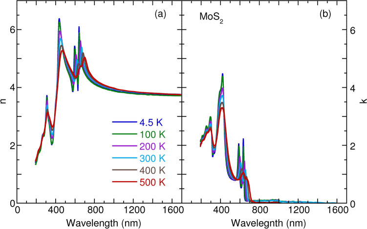
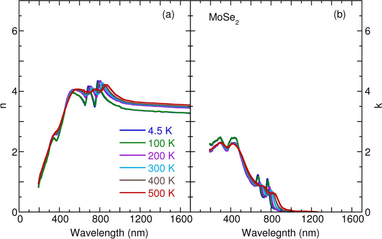
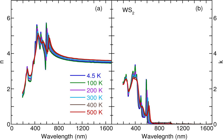
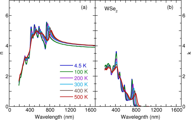
Figures 1, 2, 3 and 4 detail the observed temperature dependence of refractive index n and extinction coefficient k of monolayer , , , and as a function of the wavelength from 193 to 1700 nm. The spectra were almost identical by rotating the sample’s azimuthal orientation of and shown in the Supplementary Figs. 1 and 2, indicating the in-plane isotropic optical properties of monolayer TMDs. These data are necessary to understanding the optical properties of photonic devices for integrated optics and solar cell applications at various temperatures and wavelengths. For these four TMDs, the n increases substantially with an increase in wavelength in the spectral range from 193 to 420 nm; it then approaches several maxima, which correspond to the anomalous dispersion regime33, and finally decreases with the wavelength until 1700 nm. Moreover, the n slightly increases with an increase in temperature in the near-infrared region. The thermo-optic coefficients at room temperature are , , , and at a wavelength of 1200 nm for monolayer , , , and , respectively. The small increase of n as a function of temperature is ascribed to the enhanced electron–phonon interaction with an increase in temperature, as observed for other semiconductors, such as Si, GaAs, and InP34. It is worth noting that a small jump in n between 100 and 200 K in the case of monolayer and could be associated with the activation of the phonon modes below 35. In Figs 1, 2, 3 and 4, the extinction coefficient spectra exhibit several strong absorption peaks below 800 nm. These absorptions show a redshift trend with an increase in temperature, which agrees well with semiconductors, such as GaAs, InP, AlN, and GaN36,37. A detailed analysis of temperature-dependent optical absorptions is provided later.
Figure 1.
Temperature dependence of (a) refractive index n and (b) extinction coefficient k of monolyaer .
Figure 2.
Temperature dependence of (a) refractive index n and (b) extinction coefficient k of monolyaer .
Figure 3.
Temperature dependence of (a) refractive index n and (b) extinction coefficient k of monolyaer .
Figure 4.
Temperature dependence of (a) refractive index n and (b) extinction coefficient k of monolyaer .
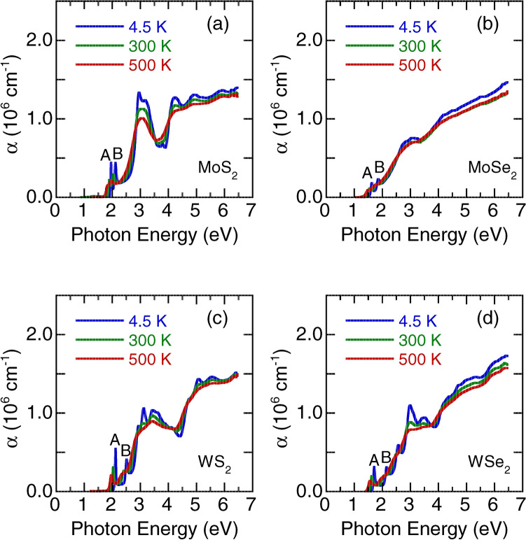
In Fig. 5, we depict the observed optical absorption coefficient of monolayer , , , and at 4.5, 300, and 500 K, respectively. The absorption can be divided into (1) a region of photon energy (1.0–2.5 eV), which is understood as excitonic transitions on a relatively low absorption background, and (2) a region of strong absorption at higher photon energies. The absorption features of monolayer above 2.5 eV are more complex than others due to strong effects of the Se p orbitals38. We fitted these absorption spectra using standard Lorentzian functions. Details of the fitting parameters at 4.5 K are provided in Supplementary Tables 1–4. The error bars in the Lorenzian fit for the measured optical absorption data are approximately 0.5%. At 4.5 K, two peaks were assigned as A and B excitons17 at approximately 1.96 and 2.12 eV, 1.62 and 1.86 eV, 2.12 and 2.51 eV, and 1.71 and 2.16 eV for the monolayer , , , and , respectively. The A and B excitons originate from the spin-split direct-gap transitions at the K point of the Brillouin zone. Thus, the spin–orbit splitting of the valence-band at the K point can be approximately estimated from the energy difference between the A and B exciton peaks. The measured spin–orbit splitting energy for was 160, 204, 390, and 450 meV for monolayer , , , and , respectively. These results are in agreement with the other theoretical predictions27,28,30,31,39–41. The measured spin–orbit splitting energy at 4.5 K was greatly enhanced in the tungsten dichalcogenides than the molybdenum counterparts. The giant spin–orbit splitting in monolayer and benefits them in potential applications in spintronics.
Figure 5.
Temperature-dependent optical absorption coefficient of monolayer (a) , (b) , (c) , and (d) . A and B denote the exciton peaks.
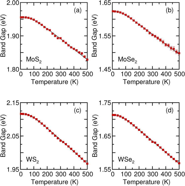
The peak positions of A and B excitons were shifted to lower energies, and their resonance linewidth increased with an increase in temperature. As illustrated in Fig. 6, we extracted the value of the optical band gap from the A exciton peak position as a function of temperature. The optical band gap describes the energy required to create an exciton, a correlated two-particle electron–hole pair, via optical absorptions for the A and B energy gaps42–45. The difference in the optical band gap of monolayer TMDs can be attributed to the difference in the chemical compositions, for example, the difference between electro-negativity (see Supplementary Fig. 3). The optical band gap decreases with an increase in temperature. The temperature dependence of the B exciton peak position is described in Supplementary Fig. 4. The observed redshift value of the optical band gap with an increase in temperature in semiconductors can be described using the Bost–Einstein model46:
| 1 |
where is the band gap energy at 0 K, represents the strength of the electron–phonon interactions, and is the average phonon temperature. In this model, the electron–phonon interactions are responsible for the shrinkage in the band gap with an increase in temperature46. In Fig. 6, the fitted values are indicated by solid lines. As in Fig. 6, the Bose–Einstein model reproduces the temperature dependence of the optical band gap in the monolayer TMDs. The parameters used to fit the temperature-dependent optical band gap are listed in Table 1. The error bars in the fit for temperature-dependent optical band gap are approximately 0.5%. Notably, in monolayer , a previous ellipsometric study determined only the linear temperature dependence of the optical band gap for 300–800 K22.
Figure 6.
Temperature-dependent optical band gap of monolayer (a) , (b) , (c) , and (d) . The thin solid lines are the results of the fitting using the Bose–Einstein model (Eq. 1).
Table 1.
The fitting parameters of the Bose–Einstein model.
| (0) (eV) | 1.99 | 1.65 | 2.15 | 1.74 |
| (meV) | 36 | 26 | 37 | 29 |
| (K) | 225 | 170 | 200 | 165 |
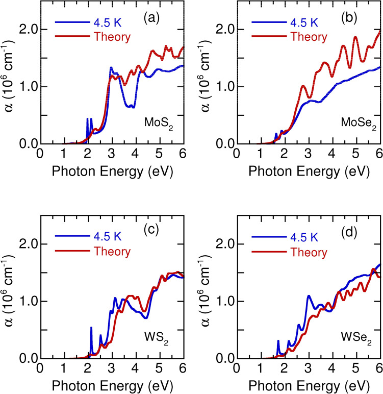
Figure 5 presents the absorption spectra for the higher photon energy regions (> 2.5 eV) of monolayer , , , and , which have a considerably higher intensity than those for the A and B exciton peaks. The assignments of the higher photon energy spectra remain controversial5,27. One study reported that these absorption bands were caused by the split excitons A’ and B’5, whereas another reported that these absorption peaks were related to strongly bound excitons27. Nevertheless, with an increase in temperature, all absorption peaks shifted to lower photon energies and broadened. To understand the origin and nature of these high energy absorption bands, we calculated the electronic band structure and optical absorption spectra43. In Fig. 7, the experimental optical absorption coefficient (blue lines) at 4.5 K is compared with the calculated (red lines) for the monolayer TMDs. Experimental n and k of monolayer , , , and at 4.5 K were also compared with the theoretical calculation curves(see Supplementary Figs. 5–8). The peak positions and general trend of in the experiment and calculation agree reasonably well. Each absorption peak corresponds to one electron–photon resonance, and all the peaks give rise to multiple resonances. The calculated results indicated that the observed strong optical absorption around 3.0 eV in the monolayer TMDs is a result of the band gap ( 2.97 eV) at the M point (the edge center point of the Brillouin zone). Usually, the M point corresponds to the van-Hove singularity point of two-dimensional materials, giving rise to a logarithmically diverging electronic density of states, which results in a large optical absorption value. The optical absorptions above 3.0 eV arose from the nested bands between the and K points, in which the joint density of states became large. We will present a more detailed analysis of the photon energy dependence of optical absorption and refractive index later within the dipole oscillator model47.
Figure 7.
Experimental optical absorption coefficient of monolayer (a) , (b) , (c) , and (d) at 4.5 K and the theoretical calculation curves.
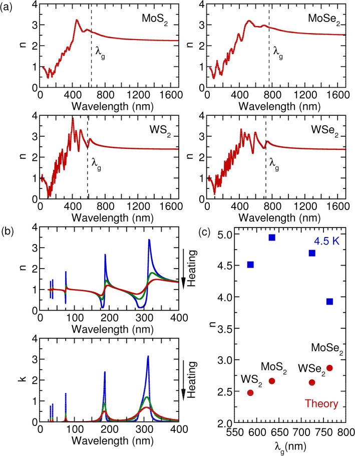
In Fig. 8, we present the calculated refractive index as a function of the wavelength of light. The calculated n appropriately reproduces the experimental data in Figs. 1, 2, 3 and 4. Two characteristics can be observed. One is that n decreases with wavelength when ( corresponds to the wavelength of the optical band gap), which is a consequence of the Kramers–Kronig relations between the real part n and imaginary part k of the complex refractive index47. The other is that n increases with wavelength but with many oscillations when . To better understand the oscillations, we employ the dipole oscillator model for multiple resonances to have a qualitative view33. Within the model, the relative dielectric index has the following form:
| 2 |
in which N is the number of dipoles per unit volume, is the reduced mass of the dipole, is the resonant frequency due to the presence of one dipole, and is the damping rate. Starting at the lowest wavelength and gradually working up to the band gap wavelength, we assume the existence of three typical resonance wavelengths as depicted in Fig. 8b. At the lowest wavelengths, or the highest frequencies, the electrons cannot follow the alternating electric fields, which provides dielectric constant unity. When we increase the wavelength and through these resonances, we observe the characteristic wavelength for dependence of the Lorentz oscillator, with a peak in the absorption spectrum and an oscillating refractive index. Between the two resonances peaks, absorption goes to zero, and n becomes a constant. The constant value of n grows with an increase in resonances when the wavelength increases. Anomalous dispersion can be appropriately interpreted within the dipole oscillator model due to multiple resonance frequencies. Also worth noting is the linear relationship between the refractive index and at the band gap for the TMDs materials, as seen in Fig. 8c. Such behavior can also be understood as indicating the Kramers–Kronig relations between n and k, usually taking the form .
Figure 8.
(a) The calculated refractive index n of monolayer TMDs. (b) Refractive index n and extinction coefficient k as a function of wavelength in dipole oscillator model with multiple resonances. The solid line with arrow in (b) indicates the increasing temperature. (c) n as a function of band gap wavelength .
The difference in the n between the experimental results and calculations in Fig. 8c can be explained as follows: (1) the results from the dipole oscillator model, as seen in Fig. 8b, indicates that the n is cumulative, and the plateau value increases stepwise from the highest frequencies to the band gap energy level. To accurately calculate the frequency-dependent dielectric function and optical absorption, an appreciable number of empty conduction states is required; however, in real calculations this number is limited, causing a decrease in the number of plateau and an underestimation of the n . (2) Local field effects (changes in the cell periodic part of potential) were neglected in the present calculation. The origins for the anomalous result of monolayer are unclear at this time. A more accurate evaluation can be applied using either density functional perturbation theory48 or the GW method49, which can be our next consideration.
To obtain an insight into the temperature dependence of the n in Figs. 1, 2, 3 and 4, we studied the temperature effect on the parameter in the dipole oscillator model, as presented in Fig. 8b. With an increase in temperature, the resonance absorption peaks decrease and broaden, as does the oscillating element of the n. However, the plateau of n does not change with temperature. The agreement between the model and experimental data indicates increasing numbers of temperature-induced phonons, which gives rise to enhanced damping .
Summary
We investigated the temperature-dependent optical constants of monolayer , , , and using spectroscopic ellipsometry. The absorption emerging in the extinction coefficient spectrum indicated that the monolayer TMDs have a direct band gap with a large exciton binding energy. With a decrease in temperature, the refractive indices decreased in the near-infrared region. The thermo-optic coefficients at room temperature ranged from to at a wavelength of 1200 nm. The optical band gap increased due to the suppression of electron–phonon interactions. The data presented in this study provide standard information for the design and fabrication of monolayer TMDs-based photonic devices for integrated optics and solar cell applications at various temperatures.
Method
Experiment
Monolayer , , , and were grown on c-axis cut sapphire substrates by ambient-pressure chemical vapor deposition with the seeding of perylene-3,4,9,10-tetracarboxylic acid tetrapotassium salt50,51. The details of sample preparation were as reported previously in Figure S2 and Table T1 of Ref.50. That these thin films were single-layer was verified by atomic force microscopy50 and Raman scattering spectroscopy (see Supplementary Fig. 9)52,53. Spectroscopic ellipsometric spectra were measured for multiple angles of incidence between and by using a J. A. Woollam Co. M-2000U ellipsometer over the spectral range from 0.73 to 6.42 eV. For the ellipsometric measurements, the multiple angles of incidence were chosen so as to maximize the difference between the intensities of the p-wave and the s-wave. In order to meet this condition, one should use an angle which is near the Brewster angle for the substrate. This is particularly important for monolayer TMDs. Because the Brewster angle for the sapphire substrate in the visible region is about , the ellipsometric spectra of monolayer TMDs were measured for multiple angles of incidence between and . The complex optical constants were obtained through spectroscopic ellipsometry using the stacked layer model (sapphire substrate/thin film/surface roughness/air ambient structure). The parameters of the model used to fit the raw ellipsometry data are listed in Table 2. The values of the mean square error (MSE) are 0.968, 1.151, 0.718, and 0.476 for monolayer , , , and , respectively. The c-axis cut sapphire substrate eliminates the inherent birefringent properties of the crystal. We adopted the optical constants of the c-axis cut sapphire substrate in the stacked layer model, which takes into account the anisotropic properties of sapphire substrate. The multiple angle of incidence spectroscopic ellipsometry is not sensitive to monolayer TMDs’ c-axis optical response because of their one-atom-thick layer. Thus, we focus on the in-plane optical properties of monolayer TMDs. Moreover, the surface roughness model automatically mixed (50/50) monolayer TMDs with vacuum (n = 1), which is similar to the approach of Bruggeman effective-medium54. The only fitting parameter is the thickness of surface roughness. The optically detected surface roughness could arise from the gradual oxidation along the grain boundaries and the adsorption of organic contaminants55. The layer thickness of TMDs obtained from the spectroscopic ellipsometry analysis was 0.6–0.7 nm, which is in good agreement with the literature data2,3,5. The independently measured experimental data at different incidence angles and the modeled curves are in good agreement (see Supplementary Figs. 10–14). Spectroscopic ellipsometric spectra were also measured between 4.5 and 500 K, for which the ellipsometer was equipped with an ultrahigh-vacuum continuous-flow liquid helium cryostat.
Table 2.
Parameters of the stacked layer model fit for the monolayer TMDs. All units are in nm.
| Thickness | 0.71 ± 0.07 | 0.70 ± 0.07 | 0.65 ± 0.07 | 0.62 ± 0.06 |
| Surface roughness | 0.07 ± 0.01 | 0.16 ± 0.02 | 0.07 ± 0.01 | 0.07 ± 0.01 |
Theoretical model
The electronic band structure and phonon dispersion relationships of monolayer , , , and were calculated using first-principles density functional theory within local density approximation as implemented in the Quantum-Espresso code56. We used the Perdew–Zunger form of the exchange-correlation functional in the local density approximation. We used the primitive cell for the calculations. The interaction between electrons and ions was described by projector augmented-wave (PAW) pseudopotentials57,58 with a plane-wave cutoff energy of 65 Ry. Fully relativistic pseudopotentials derived from an atomic Dirac-like equation59 were employed to calculate the electronic band structure with spin–orbit interaction considered. The atomic structure was optimized with an atomic force of less than Ry/Bohr. A k-mesh of under the Monkhorst–Pack scheme60 was used to sample the Brillouin zone. The phonon dispersion relationship of monolayer TMDs was calculated using density functional perturbation theory61.
The electronic band structures of monolayer TMDs were given in our previous results and can be referred to Ref.35,52,53. The frequency-dependent dielectric matrix was calculated using the electronic ground state. The imaginary part was determined by a summation over empty states using the equation62:
| 3 |
where is the volume of the primitive cell, is the k-point weight defined such that they sum to 1 for occupied states, c and v refer to conduction and valence band states, respectively, and (, v) is the periodic part of the orbitals at each k point. The vectors are unit vectors for the three Cartesian directions. The real dielectric tensor was obtained using the conventional Kramers–Kronig transformation. Considering that the calculation of the superlattice dielectric function in Eq. (3) can be highly sensitive to interlayer spacing along the perpendicular axis63, we have calculated the electric fields required to compensate the dipole of the system at each iteration of the self-consistency cycle. The potential added to the grid corresponds to that of a dipole layer at the middle of the vacuum layer. For slabs, this exactly compensates the electric fields at the vacuum created by the dipole moment of the system, thus allowing to treat asymmetric slabs and to compute optical properties more properly.
The refractive index and optical absorption spectrum were calculated using the real () and imaginary () parts of the dielectric function as a function of photon energy, following the PAW methodology62. The refractive index . The extinction coefficient64 . The absorption coefficient is described by , where E is the photon energy, h is the Planck constant, and c is the speed of light.
Supplementary information
Acknowledgements
H.L.L. thanks the Ministry of Science and Technology of Republic of China for its financial support under Grant-MOST 108-2112-M-003-013. T.Y. acknowledges the National Key R&D Program of China (2017YFA0206301) and the Major Program of Aerospace Advanced Manufacturing Technology Research Foundation NSFC and CASC, China (U1537204). H.G. acknowledges NSFC grant-51702146 and the Liaoning Province Doctor Startup Fund (201601325). R.S. acknowledges MEXT-Japan for Grant-JP18H01810. L.J.L. thanks the Taiwan Consortium of Emergent Crystalline Materials (TCECM), the Ministry of Science and Technology, and USA AFOSR BRI (FA238615100015).
Author contributions
H.L.L. conceived the idea and designed the experiments. J.H.C. and H.W.C. conducted the experiments. M.Y.L. and L.J. L. prepared the samples. T.Y., H.G., and R.S. performed the first-principles calculations and theoretical analyses. H.L.L. and T.Y. wrote the paper. All the authors discussed the results and commented on the manuscript.
Data availability
The data that support the findings of this study are available from the corresponding author upon reasonable request.
Competing interests
The authors declare no competing interests.
Footnotes
Publisher's note
Springer Nature remains neutral with regard to jurisdictional claims in published maps and institutional affiliations.
Contributor Information
Hsiang-Lin Liu, Email: hliu@ntnu.edu.tw.
Teng Yang, Email: yangteng@imr.ac.cn.
Supplementary information
is available for this paper at 10.1038/s41598-020-71808-y.
References
- 1.Mak KF, Lee C, Hone J, Shan J, Heinz TF. Atomically thin MoS2: a new direct-gap semiconductor. Phys. Rev. Lett. 2010;105:136805. doi: 10.1103/PhysRevLett.105.136805. [DOI] [PubMed] [Google Scholar]
- 2.Splendiani A, Sun L, Zhang Y, Li T, Kim J, Chim CY, Galli G, Wang F. Emerging photoluminescence in monolayer . Nano Lett. 2010;10:1271. doi: 10.1021/nl903868w. [DOI] [PubMed] [Google Scholar]
- 3.Tongay S, Zhou J, Ataca C, Lo K, Matthews TS, Li J, Grossman JC, Wu J. Thermally driven crossover from indirect toward direct bandgap in 2D semiconductors: versus . Nano Lett. 2012;12:5576. doi: 10.1021/nl302584w. [DOI] [PubMed] [Google Scholar]
- 4.Gutuerrez HR, P.-Lopez N, Elias AL, Berkdemir A, Wang B, L.-Urias RLF, Crespi VH, Terrones H, Terrones M. Extraordinary room-temperature photoluminescence in triangular monolayers. Nano Lett. 2013;13:3447. doi: 10.1021/nl3026357. [DOI] [PubMed] [Google Scholar]
- 5.Zhao W, Ghorannevis Z, Chu L, Toh M, Kloc C, Tan PH, Eda G. Evolution of electronic structure in atomically thin sheets of and . ACS Nano. 2013;7:791. doi: 10.1021/nn305275h. [DOI] [PubMed] [Google Scholar]
- 6.Yoon Y, Ganapathi K, Salahuddin S. How good can monolayer transistors be? Nano Lett. 2011;11:3768. doi: 10.1021/nl2018178. [DOI] [PubMed] [Google Scholar]
- 7.Radisavljevic B, Radenovic A, Brivio J, Giacometti V, Kis A. Single-layer transistors. Nat. Nanotechnol. 2011;6:147. doi: 10.1038/nnano.2010.279. [DOI] [PubMed] [Google Scholar]
- 8.Radisavljevic B, Whitwick MB, Kis A. Integrated circuits and logic operations based on single-layer . ACS Nano. 2011;5:9934. doi: 10.1021/nn203715c. [DOI] [PubMed] [Google Scholar]
- 9.Wang QH, Kourosh KZ, Kis A, Coleman JN, Strano MS. Electronics and optoelectronics of two-dimensional transition metal dichalcogenides. Nat. Nanotechnol. 2012;7:699. doi: 10.1038/nnano.2012.193. [DOI] [PubMed] [Google Scholar]
- 10.Chhowalla M, Shin HS, Eda G, Li LJ, Loh KP, Zhang H. The chemistry of two-dimensional layered transition metal dichalcogenides nanosheets. Nat. Chem. 2013;5:263. doi: 10.1038/nchem.1589. [DOI] [PubMed] [Google Scholar]
- 11.Larentis S, Fallahazad B, Tutuc E. Field-effect transistors and intrinsic mobility in ultra-thin layers. Appl. Phys. Lett. 2012;101:223104. [Google Scholar]
- 12.Bernardi M, Palummo M, Grossman JC. Extraordinary sunlight absorption and one nanometer thick photovoltaics using two-dimensional monolayer materials. Nano Lett. 2013;13:3664. doi: 10.1021/nl401544y. [DOI] [PubMed] [Google Scholar]
- 13.Zhang W, Huang JK, Chen CH, Chang YH, Chen YJ, Li LJ. High-gain phototransistors based on a CVD monolayer. Adv. Mater. 2013;25:3456. doi: 10.1002/adma.201301244. [DOI] [PubMed] [Google Scholar]
- 14.Xia F, Wang H, Xiao D, Dubey M, Ramasubramaniam A. Two-dimensional material nanophotonics. Nat. Photonics. 2014;8:899. [Google Scholar]
- 15.Eginligil M, Cao B, Wang Z, Shen S, Cong C, Shang J, Soci C, Yu T. Dichroic spin-valley photocurrent in monolayer molybdenum disulphide. Nat. Commun. 2015;6:7636. doi: 10.1038/ncomms8636. [DOI] [PMC free article] [PubMed] [Google Scholar]
- 16.Ye Y, Xiao J, Wang H, Ye Z, Zhu H, Zhao M, Wang Y, Zhao J, Yin X, Zhang X. Electrical generation and control of the valley carriers in a monolayer transition metal dichalcogenide. Nat. Nanotechnol. 2016;11:598. doi: 10.1038/nnano.2016.49. [DOI] [PubMed] [Google Scholar]
- 17.Liu HL, Shen CC, Su SH, Hsu CL, Li MY, Li LJ. Optical properties of monolayer transition metal dichalcogenides probed by spectroscopic ellipsometry. Appl. Phys. Lett. 2014;105:201905. [Google Scholar]
- 18.Tompkins HG, McGahan WA. Spectroscopic Ellipsometry and Reflectometry: A Users Guide. New York: Wiley; 1999. [Google Scholar]
- 19.Yim CY, O’Brien M, McEvoy N, Winters S, Mirza I, Lunney JG, Duesberg GS. Investigation of the optical properties of thin films using spectroscopic ellipsometry. Appl. Phys. Lett. 2014;104:103114. [Google Scholar]
- 20.Eichfeld SM, Eichfeld CM, Lin Y-C, Hossain L, Robinson JA. Rapid, non-destructive evaluation of ultrathin using spectroscopic ellipsometry. Appl. Mater. 2014;2:092508. [Google Scholar]
- 21.Park HG, Kim TJ, Kim HS, Yoo CH, Barange NS, Le VL, Kim HU, Senthilkumar V, Le CT, Kim YS, Seong M-J, Kim YD. Temperature dependence of the critical points of monolayer by ellipsometry. Appl. Spectrosc. Rev. 2016;51:621. [Google Scholar]
- 22.Choi BK, Kim M, Jung K-H, Kim J, Yu K-S, Chang YJ. Temperature dependence of band gap in grown by molecular beam epitaxy. Nanoscale Res. Lett. 2017;12:492. doi: 10.1186/s11671-017-2266-7. [DOI] [PMC free article] [PubMed] [Google Scholar]
- 23.Huang, K., & Rhys, A. Theory of light absorption and non-radiative transitions in F-centres. In Proceedings of the Royal Society, London, Series A 204, Mathematical, Physical and Engineering Sciences. The Royal Society, p. 406 (1950).
- 24.Diware MS, Ganorkar SP, Park K, Chegal W, Cho HM, Cho YJ, Kim YD, Kim H. Dielectric function, critical points, and Rydberg exciton series of monolayer. J. Phys.: Condnes. Matter. 2018;30:235701. doi: 10.1088/1361-648X/aac187. [DOI] [PubMed] [Google Scholar]
- 25.Park HG, Kim TJ, Ullah F, Le VL, Nguyen HT, Kim YS, Kim YD. Temperature dependence of the dielectric function of monolayer . Sci. Rep. 2018;8:3173. doi: 10.1038/s41598-018-21508-5. [DOI] [PMC free article] [PubMed] [Google Scholar]
- 26.Elliott JD, Xu ZM, Umari P, Jayaswal G, Chen MG, Zhang XX, Martucci A, Marsili M, Merano M. Surface susceptibility and conductivity of and monolayer: A first-principles and ellipsometry characterization. Phys. Rev. B. 2020;101:045414. [Google Scholar]
- 27.Molina-Sanchez A, Sangalli D, Hummer K, Marini A, Wirtz L. Effect of spin-orbit interaction on the optical spectra of single-layer, double-layer, and bulk . Phys. Rev. B. 2013;88:045412. [Google Scholar]
- 28.Qiu DY, da Jornada FH, Louie SG. Optical spectrum of : many-body effects and diversity of exciton states. Phys. Rev. Lett. 2013;111:216805. doi: 10.1103/PhysRevLett.111.216805. [DOI] [PubMed] [Google Scholar]
- 29.Qiu DY, da Jornada FH, Louie SG. Optical spectrum of : many-body effects and diversity of exciton states. Phys. Rev. Lett. 2015;115:119901(E). doi: 10.1103/PhysRevLett.111.216805. [DOI] [PubMed] [Google Scholar]
- 30.Zhu ZY, Cheng YC, Schwingenschlöl U. Giant spin-orbit-induced spin splitting in two-dimensional transition-metal dichalcogenide semiconductors. Phy. Rev. B. 2011;84:153402. [Google Scholar]
- 31.Ramasubramaniam A. Large excitonic effects in monolayers of molybdenum and tungsten dichalcogenides. Phys. Rev. B. 2012;86:115409. [Google Scholar]
- 32.Rukelj Z, Štrkalj A, Despoja V. Phys. Rev. B. 2016;94:115428. [Google Scholar]
- 33.Hecht E. Optics. San Francisco: Addison Wesley; 2002. [Google Scholar]
- 34.McCaulley JA, Donnelly VM, Vernon M, Taha I. Temperature dependence of the near-infrared refractive index of silicon. gallium arsenide, and indium phosphide. Phys. Rev. B. 1994;49:7408. doi: 10.1103/physrevb.49.7408. [DOI] [PubMed] [Google Scholar]
- 35.Saito R, Nugraha ART, Hasdeo EH, Siregar S, Guo HH, Yang T. Ultraviolet Raman spectroscopy of graphene and transition-metal dichalcogenides. Phys. Status Solidi B. 2015;252:2363. [Google Scholar]
- 36.Beaudoin M, DeVries AJG, Johnson SR, Laman H, Tiedje T. Optical absorption edge of semi-insulating GaAs and InP at high temperature. Appl. Phys. Lett. 1997;70:3540. [Google Scholar]
- 37.Nam KB, Li J, Lin JY, Jiang HX. Optical properties of AlN and GaN in elevated temperatures. Appl. Phys. Lett. 2004;85:3489. [Google Scholar]
- 38.Beal AR, Knights JC, Liang WY. Transmission spectra of some transition metal dichalcogenides. II. Group VIA: trigonal prismatic coordination. J. Phys. C: Solid State Phys. 1972;5:3540. [Google Scholar]
- 39.Cheiwchanchamnangij T, Lambrecht WRL. Quasiparticle band structure calculation of monolayer, bilayer, and bulk . Phys. Rev. B. 2012;85:205302. [Google Scholar]
- 40.Komsa HP, Kresheninnikov AV. Effects of confinement and environment on the electronic structure and exciton binding energy of from first principles. Phys. Rev. B. 2012;86:241201. [Google Scholar]
- 41.Shi H, Pan H, Zhang YW, Yakobson BI. Quasiparticle band structure and optical properties of strained monolayer and . Phys. Rev. B. 2013;87:155304. [Google Scholar]
- 42.Ugeda MM, Bradley AJ, Shi SF, da Jornada FH, Zhang Y, Qiu DY, Ruan W, Mo SK, Hussain Z, Shen ZX, Wang F, Louie SG, Crommie MF. Giant bandgap renormalizatoin and excitonic effects in a monolayer transition metal dichalcogenides semiconductor. Nat. Mater. 2014;13:1091. doi: 10.1038/nmat4061. [DOI] [PubMed] [Google Scholar]
- 43.Tastumi Y, Ghalamkari K, Saito R. Laser energy dependence of valley polarization in transition-metal dichalcogenides. Phys. Rev. B. 2016;94:235408. [Google Scholar]
- 44.Kozawa D, Kumar R, Carvalho A, Amara KK, Zhao WJ, Wang SF, Toh ML, Ribeiro RM, Castro Neto AH, Mastuda K, Eda G. Photocarrier relaxation pathway in two-dimensional semiconducting transition metal dichalcogenides. Nat. Commun. 2014;5:4543. doi: 10.1038/ncomms5543. [DOI] [PubMed] [Google Scholar]
- 45.Zeng HL, Cui XD. An optical spectroscopic study on two-dimensional group-VI transition metal dichalcogenides. Chem. Soc. Rev. 2015;44:2629. doi: 10.1039/c4cs00265b. [DOI] [PubMed] [Google Scholar]
- 46.Vina L, Logotheridis S, Cardona M. Temperature dependence of the dielectric function of germanium. Phys. Rev. B. 1984;30:1979. [Google Scholar]
- 47.Fox M. Optical Properties of Solids. New York: Oxford University Press; 2010. [Google Scholar]
- 48.Baroni S, Resta R. Ab initio calculation of the macroscopic dielectric constant in silicon. Phys. Rev. B. 1986;33:7017. doi: 10.1103/physrevb.33.7017. [DOI] [PubMed] [Google Scholar]
- 49.Shishkin M, Kresse G. Self-consistent GW calculations for semiconductors and insulators. Phys. Rev. B. 2007;75:235102. doi: 10.1103/PhysRevLett.99.246403. [DOI] [PubMed] [Google Scholar]
- 50.Lee YH, Yu L, Wang H, Fang W, Ling X, Shi Y, Lin CT, Huang JK, Chang MT, Chang CS, Dresselhaus M, Palacios T, Li LJ, Kong J. Synthesis and transfer of single-layer transition metal disulfides on diverse surfaces. Nano Lett. 2013;13:1852. doi: 10.1021/nl400687n. [DOI] [PubMed] [Google Scholar]
- 51.Shi YM, Li HN, Li LJ. Recent advances in controlled synthesis of two-dimensional transition metal dichalcogenides via vapour deposition techniques. Chem. Soc. Rev. 2015;44:2744. doi: 10.1039/c4cs00256c. [DOI] [PubMed] [Google Scholar]
- 52.Liu HL, Guo HH, Yang T, Zhang ZD, Kumamoto Y, Shen CC, Hsu YT, Li LJ, Saito R, Kawata S. Anomalous lattice vibrations of monolayer probed by ultraviolet Raman scattering. Phys. Chem. Chem. Phys. 2015;17:14561. doi: 10.1039/c5cp01347j. [DOI] [PubMed] [Google Scholar]
- 53.Liu HL, Yang T, Tatsumi Y, Zhang Y, Dong BJ, Guo HH, Zhang ZD, Kumamoto Y, Li MY, Li LJ, Saito R, Kawata S. Deep-ultraviolet Raman scattering spectroscopy of monolayer . Sci. Rep. 2018;8:11398. doi: 10.1038/s41598-018-29587-0. [DOI] [PMC free article] [PubMed] [Google Scholar]
- 54.Bruggeman DAG. Berechnung verschiedener physikalischer Konstanten von heterogenen Substanzen. I. Dielektrizitätskonstanten und Leitfähigkeiten der Mischkörper aus isotropen Substanzen. Ann. Phys. 1935;24:636. [Google Scholar]
- 55.Gao J, Li BC, Tan JW, Chow P, Lu T-M, Koratkar N. Aging of transition metal dichalcogenide monolayers. ACS Nano. 2016;10:2628. doi: 10.1021/acsnano.5b07677. [DOI] [PubMed] [Google Scholar]
- 56.Giannozzi P, Baroni S, Bonini N, Calandra M, Car R, Cavazzoni C, Ceresoli D, Chiarotti GL, Cococcioni M, Dabo I, Corso AD, de Gironcoli S, Fabris S, Fratesi G, Gebauer R, Gerstmann W, Gougoussis C, Kokalj A, Lazzeri M, Martin-Samos L, Marzari N, Mauri F, Mazzarello R, Paolini S, Pasquarello A, Paulatoo L, Sbraccia C, Scandolo S, Sclauzero G, Sbraccia C, Scandolo S, Sclauzero G, Seitsonen AP, Smogunov A, Umari P, Wentzcovitvh RM. QUANTUM ESPRESSO: a modular and open-source software project for quantum simulations of materials. J. Phys.: Condens. Matter. 2009;21:395502. doi: 10.1088/0953-8984/21/39/395502. [DOI] [PubMed] [Google Scholar]
- 57.Kresse G, Joubert D. From ultrasoft pseudopotentials to the projector augmented-wave method. Phys. Rev. B. 1999;59:1758. [Google Scholar]
- 58.Blöchl PE. Projector augmented-wave method. Phys. Rev. B. 1994;50:17953. doi: 10.1103/physrevb.50.17953. [DOI] [PubMed] [Google Scholar]
- 59.Theurich G, Hill NA. Self-consistent treatment of spin-orbit coupling in solids using relativistic fully separable ab initio pseudopotentials. Phys. Rev. B. 2001;64:073106. [Google Scholar]
- 60.Monkhorst HJ, Pack JD. Special points for Brillouin-zone integrations. Phys. Rev. B. 1976;13:5188. [Google Scholar]
- 61.Baroni S, de Gironcoli S, Corso AD, Giannozzi P. Phonons and related crystal properties from density-functional perturbation theory. Rev. Mod. Phys. 2001;73:515. [Google Scholar]
- 62.Gajdoš M, Hummer K, Kresse G, Furthmüller J, Bechstedt F. Linear optical properties in the projector-augmented wave methodology. Phys. Rev. B. 2006;73:045112. [Google Scholar]
- 63.Matthes L, Pulci O, Bechstedt F. Influence of out-of-plane response on optical properties of two-dimensional materials: first principles approach. Phys. Rev. B. 2016;94:205408. [Google Scholar]
- 64.Zimmermann H. Integrated Silicon Optoelectronics, Springer Series in Optical Sciences. New York: Springer; 2000. [Google Scholar]
Associated Data
This section collects any data citations, data availability statements, or supplementary materials included in this article.
Supplementary Materials
Data Availability Statement
The data that support the findings of this study are available from the corresponding author upon reasonable request.


