Abstract
PtSe2 has received substantial research attention because of its intriguing physical properties and potential practical applications. In this paper, we investigated the optical properties of bilayer and multilayer PtSe2 thin films through spectroscopic ellipsometry over a spectral range of 0.73–6.42 eV and at temperatures between 4.5 and 500 K. At room temperature, the spectra of refractive index exhibited several anomalous dispersion features below 1000 nm and approached a constant value in the near-infrared frequency range. The thermo-optic coefficients of bilayer and multilayer PtSe2 thin films were (4.31 ± 0.04) × 10−4/K and (–9.20 ± 0.03) × 10−4/K at a wavelength of 1200 nm. Analysis of the optical absorption spectrum at room temperature confirmed that bilayer PtSe2 thin films had an indirect band gap of approximately 0.75 ± 0.01 eV, whereas multilayer PtSe2 thin films exhibited semimetal behavior. The band gap of bilayer PtSe2 thin films increased to 0.83 ± 0.01 eV at 4.5 K because of the suppression of electron–phonon interactions. Furthermore, the frequency shifts of Raman-active Eg and A1g phonon modes of both thin films in the temperature range between 10 and 500 K accorded with the predictions of the anharmonic model. These results provide basic information for the technological development of PtSe2-based optoelectronic and photonic devices at various temperatures.
Subject terms: Materials science, Nanoscience and technology, Optics and photonics
Introduction
Two-dimensional transition-metal dichalcogenides (TMDs) have attracted considerable attention because of their novel physical properties in the reduced dimension and potential practical applications1–5. TMDs (common formula MX2 [M = Mo, W; X = S, Se]) possess substantial band gap energies (approximately 1.0 to 2.0 eV) because of their quantum confinement effect and weak van der Waals forces3,6–10. Subsequent studies11–13 have revealed that these characterizations can be altered simply by tuning their thickness. Furthermore, indirect to direct band gap transitions occur when the thickness is reduced to a monolayer. Additionally, TMDs exhibit high carrier mobility and high quantum efficiency of photoluminescence yield12,14,15. These superior properties make TMDs very attractive materials for use in optoelectronics16, photovoltaic17, and field-effect transistors18.
PtSe2 has received much research interest as an emerging TMDs material19. It exhibits unique thickness-dependent type-II Dirac semimetal to semiconducting transition20,21. Moreover, PtSe2 exhibits strong interlayer coupling and excellent carrier mobility22. It is a promising material for use in next-generation sensors, optoelectronics, and ultrafast photonic devices23–25. Circular polarization calculations have revealed that single-layer PtSe2 exhibits strong circular dichroism polarization along the M–K direction and near the Γ point. Thus, PtSe2 is an excellent candidate for valleytronic devices26. In light of the many potential applications of PtSe2, a comprehensive study of optical properties for PtSe2 is essential. The temperature-dependent optical constants of PtSe2 are critical references for determining the effects of self-heating on a device. O’Brien et al.27 studied the Raman scattering spectra of direct-selenization grown PtSe2 thin films as a function of film thickness, laser wavelength, and laser polarization. They found that the positions of phonon modes of PtSe2 thin films exhibited a redshift with increase in the thickness from 0.5 to 5.0 nm. This phenomenon was attributed to domination of stacking-induced structural changes and Columbic interaction effects when the number of layers of the PtSe2 thin films was increased. Yu et al.28 reported that PtSe2 thin films possess variable band gaps in the mid-infrared frequency region. They showed that monolayer PtSe2 is suitable for use in visible and near-infrared photodetectors. Thus, bilayer PtSe2 thin films are compatible with mid-infrared photodetectors and are an excellent candidate for photoelectronic devices. Xie et al.29 investigated the room-temperature optical constants of PtSe2 for different thicknesses through spectroscopic ellipsometry. They found that the values of refractive index and extinction coefficient exhibited a strong dependence on thickness.
Most optical measurements of PtSe2 thin films have been limited to room temperature27–29. The temperature-dependent optical properties of PtSe2 thin films have not been reported. In this paper, we characterized the optical constants of PtSe2 thin films over a wide range of photon energy (from 0.73 to 6.42 eV) and temperature (between 4.5 and 500 K) through spectroscopic ellipsometry. We found that bilayer PtSe2 thin films exhibited an indirect band gap and that multilayer PtSe2 thin films exhibited semimetal behavior at 300 K. Furthermore, the band gap of bilayer PtSe2 thin films increased from 0.71 ± 0.01 to 0.83 ± 0.01 eV when temperature decreased from 500 to 4.5 K. Multilayer PtSe2 thin films exhibited a band gap of approximately 0.04 ± 0.004 eV at 500 K. Additionally, we investigated the temperature-dependent Raman scattering spectra of PtSe2 thin films from 10 to 500 K. The temperature dependence of Eg and A1g phonon modes was attributed to the anharmonic contributions to the interatomic potential energy, mediated by phonon–phonon interactions. These findings are highly promising for further development of PtSe2 thin films in optoelectronic and photonic applications at various temperatures.
Experiment
Bilayer and multilayer PtSe2 thin films were grown on sapphire substrates by using chemical vapor deposition method. Platinum (II) chloride (PtCl2) and selenium (Se) were used as precursors. Both PtSe2 samples with an area of approximately 1 cm2 were formed at a temperature of 400 °C. The growth time ranged from 10 to 20 min for bilayer and multilayer thin films, respectively. The samples were prepared according to the method described in21. Figure 1 depicts the optical microscopic and atomic force microscopic images, and corresponding height profiles of two thin films. The thickness of these two thin films was approximately 1.4 and 5.0 nm, respectively, thus corresponding to two and seven PtSe2 layers. Both thin films were also verified through transmission electron microscopy to be high-quality samples30.
Figure 1.
(a) Optical microscopic images of two PtSe2 thin films. (b–e) Atomic force microscopic images and corresponding height profiles of two PtSe2 thin films.
Room-temperature spectroscopic ellipsometry spectra were recorded under incident angles of 60°, 65°, 70°, and 75° and over a spectral range of 0.73 to 6.42 eV by using an ellipsometer (J. A. Woollam Co. M-2000U). For temperature-dependent measurements between 4.5 and 500 K, the samples were placed in a Janis ST-400 ultrahigh-vacuum continuous-flow helium cryostat31,32. The optical constants were obtained through spectroscopic ellipsometry using the stacked layer model (sapphire substrate/thin film/surface roughness/air ambient structure)32. The parameters of the model used to fit the raw ellipsometry data are listed in Table 1. The values of the mean square error are 1.07 and 1.40 for bilayer and multilayer PtSe2 thin films. The independently measured experimental data at different incident angles and modeled curves exhibited good agreement (see Supplementary Figs. 1 and 2).
Table 1.
Parameters of the stacked layer model fit for bilayer and multilayer PtSe2 thin films.
| Layer type | Bilayer | Multilayer |
|---|---|---|
| Sapphire substrate (mm) | 1 | 1 |
| Film (nm) | 1.45 ± 0.3 | 5.10 ± 0.6 |
| Surface roughness (nm) | 0.10 ± 0.02 | 0.25 ± 0.03 |
Figure 2.
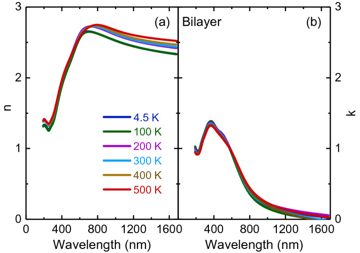
Temperature-dependent (a) refractive index and (b) extinction coefficient of bilayer PtSe2 thin film.
Room-temperature micro-Raman scattering measurements were performed using a backscattering geometry with a laser excitation wavelength of 532 nm31. The linear polarized light was focused to a 3-μm-diameter spot on the sample surface. Subsequently, a SENTERRA spectrometer collected and dispersed the scattered light with a 1024-pixel-wide charge-coupled detector. The spectral resolution achieved using these instruments was generally less than 0.5 cm−1. To avoid heating effects, the laser power was set to less than 0.5 mW. The sapphire substrate exhibited high thermal conductivity and evacuated heating well33. The samples were mounted in a continuous-flow helium cryostat and LINKAM heating stage, which enabled measurements in the temperature range of 10–500 K31.
Results and discussion
Figures 2 and 3 illustrate the temperature-dependent optical constant spectra of bilayer and multilayer PtSe2 thin films recorded in a wavelength range of 193 to 1700 nm obtained through spectroscopic ellipsometry analysis. The spectra were almost identical by rotating the sample’s azimuthal orientation of 45° and 90° shown in the Supplementary Figs. 3 and 4, indicating the in-plane isotropic optical properties of PtSe2 thin films. For both thin films, the room-temperature refractive index increased substantially with an increase in the wavelength in the spectral range from 193 to 700 nm for bilayer and from 193 to 1100 nm for multilayer thin films. It then approached one maximum, which corresponded with the anomalous dispersion regime34 and finally decreased with the wavelength until the wavelength reached 1700 nm. With an increase in layer thickness, the value of refractive index increased. This phenomenon is consistent with previous reports of thickness-dependent optical constants29. Notably, multilayer PtSe2 thin film exhibited large refractive index values (approximately 6.88 at a wavelength of 1070 nm). Bilayer PtSe2 thin film exhibited a maximum refractive index of approximately 2.72 at a wavelength of 720 nm. The characteristics of high refractive indices of bilayer and multilayer PtSe2 thin films indicated a large scattering cross-section inside the crystal35. Thus, these effects are highly favorable for light trapping in photonic36 and optoelectronic37 devices in the visible to near-infrared frequency range. With a decrease in temperature, the refractive index of bilayer PtSe2 thin film decreased in the near-infrared region. This behavior is ascribed to the decreased electron–phonon interaction with a decrease in temperature, as observed for other semiconducting TMDs, such as monolayer MoS2, MoSe2, WS2, and WSe232. By contrast, this trend was reversed for multilayer PtSe2 thin film, which could be associated with the enhanced electron–phonon interaction. The thermo-optic coefficients (∂n/∂T) for bilayer and multilayer PtSe2 thin films were (4.31 ± 0.04) × 10−4/K and (− 9.20 ± 0.03) × 10−4/K, respectively, at a wavelength of 1200 nm. Bilayer PtSe2 thin film exhibited a positive thermo-optic coefficient value, similar to the coefficient of other semiconducting materials such as silicon38. By contrast, multilayer PtSe2 thin film had a negative value of thermo-optic coefficient that was similar to the coefficient of TiO239. The negative thermo-optic coefficient observed in multilayer PtSe2 may arise from the enhanced electron–phonon interaction at low temperatures because of its semimetallic properties. The extinction coefficient spectra (Figs. 2 and 3) of two thin films were featureless above 1000 nm, but exhibited several absorption peaks below 1000 nm. These absorptions exhibited a blueshift trend with a decrease in temperature. A detailed analysis of temperature-dependent optical absorption is provided later.
Figure 3.
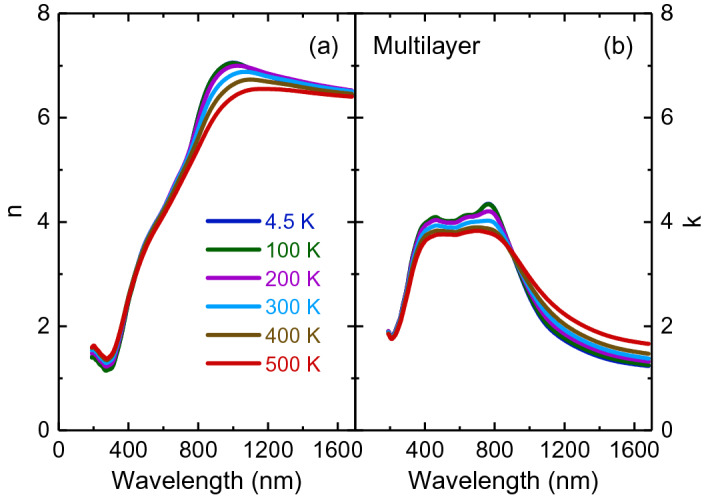
Temperature-dependent (a) refractive index and (b) extinction coefficient of multilayer PtSe2 thin film.
Figure 4.
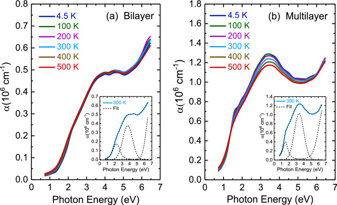
Temperature-dependent optical absorption spectra of (a) bilayer and (b) multilayer PtSe2 thin films. The inset illustrates the best fit using the Lorentz-Gaussian function at 300 K.
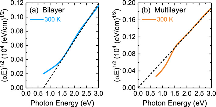
Figure 4 presents the temperature-dependent optical absorption coefficient spectra of two thin films. The absorption spectra were fitted using the Lorentzian-Gaussian function, as illustrated by the dashed lines in the inset of Fig. 4. Bilayer PtSe2 thin film exhibited two optical absorption bands at approximately 2.22 and 3.75 eV. Multilayer PtSe2 thin film revealed two optical absorption bands at approximately 1.51 and 3.39 eV. In accordance with previous reports20,40, all absorption peaks for two thin films were assigned to charge-transfer excitations between the hybridization of Pt 5d and Se 4p states at the valence and conduction band edges. Moreover, the first-principles calculations20 predicted that the rapid decrease in band energy of conduction band states and increase in valence band states lead to metallization starting from trilayer PtSe2 thin film. As a result, two absorption bands observed in multilayer PtSe2 thin film exhibited a redshift as compared to those of bilayer PtSe2 thin film. The band gap energy of bilayer and multilayer PtSe2 thin films is depicted Fig. 5. The optical absorption coefficient, which includes contributions from both direct and indirect band gap transitions, was analyzed using the following expression41:
| 1 |
where Eg,dir and Eg,ind are the magnitudes of direct and indirect band gaps, respectively; Eph is the emitted (absorbed) phonon energy, and A and B are constants. This model, which assumes a simple band shape, enables extraction of the direct band gap when (α·E)2 is plotted as a function of photon energy and extraction of indirect band gap when (α·E)1/2 is plotted as a function of photon energy. Figure 5 presents an indirect band gap of approximately 0.75 ± 0.01 eV at 300 K for bilayer PtSe2 thin film, whereas multilayer PtSe2 thin film exhibited semimetal behavior from 300 to 4.5 K (see Supplementary Fig. 5). Plotting (α·E)2 as a function of photon energy for both thin films led to a negative value for the band gap. The results of our band gap analysis of bilayer PtSe2 thin film were consistent with those of other experimental studies29,41,42. However, the results for multilayer PtSe2 thin film differed from those of other reports of semiconducting behavior in films of a similar thickness29,42,43. One possibility that could account for these differences is due to different quality of thin films.
Figure 5.
The plot of (α·E)1/2 vs. photon energy enables the extraction of indirect band gap of (a) bilayer and (b) multilayer PtSe2 thin films at 300 K.
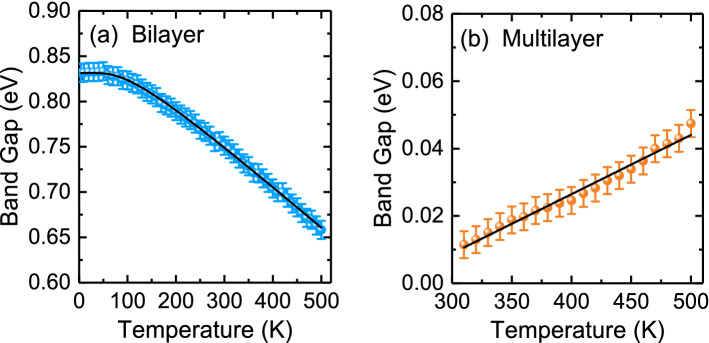
Figure 6 displays the temperature dependence of the band gap of bilayer and multilayer PtSe2 thin films. The band gap of bilayer PtSe2 thin film increased with a decrease in temperature. The observed blueshift value of the band gap energy with decreasing temperature in semiconductors can be described using the Bose–Einstein model as follows44:
| 2 |
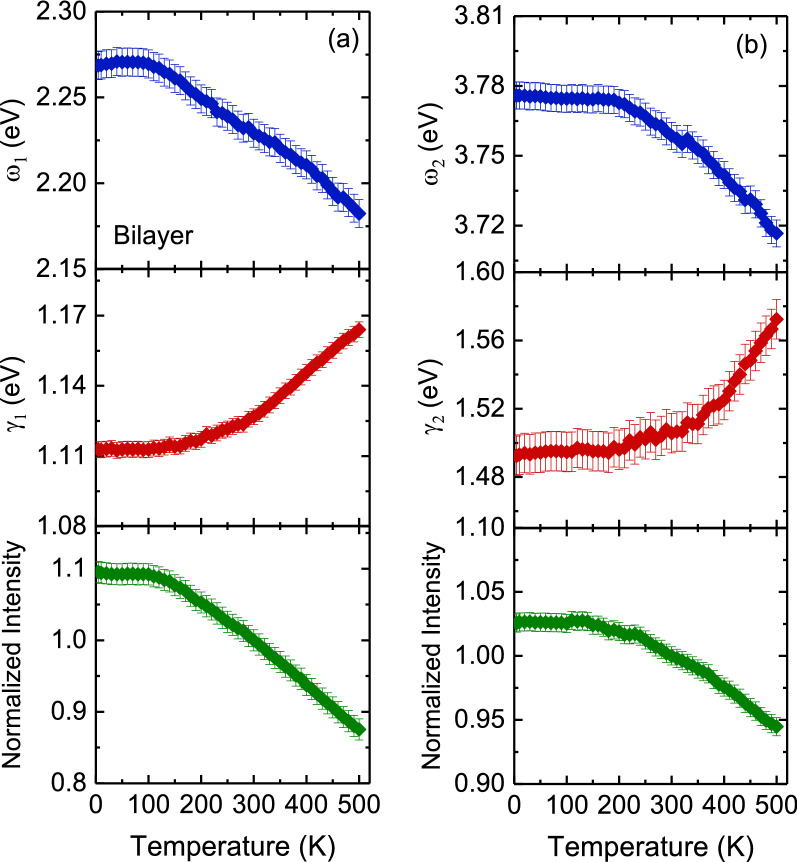
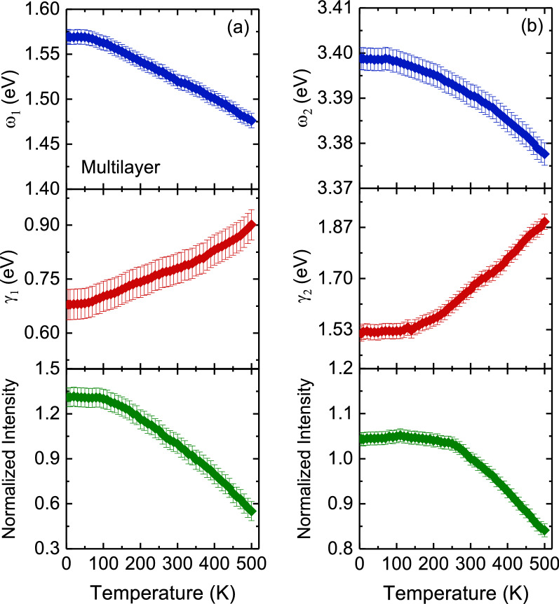
where Eg (0) represents the band gap at 0 K, is the strength of the electron–phonon interactions, and is the average phonon temperature. Our fitting results indicated that the band gap energy toward 0 K was approximately 0.83 ± 0.01 eV. The strength of the electron–phonon interactions aB and the average phonon temperature ΘB were 66 meV and 288 K, respectively. These values are comparable to those obtained for other semiconducting materials such as ZnS45 and ZnSe46. In contrast to bilayer PtSe2 thin film, multilayer PtSe2 thin film revealed a band gap energy that steadily increased with an increase in temperature from 310 to 500 K. This could induce semimetal to semiconducting transition and may be due to both the electron–phonon interaction and thermal expansion of the lattice47. The linearly fitted result indicated that the temperature coefficient was 1.75 × 10⁻⁴ eV/K. This value is lower than those of other TMDs such as ReS248. Figures 7 and 8 illustrate the peak energy, damping, and normalized intensity of 2.22- and 3.75-eV optical transitions for bilayer PtSe2 thin film and 1.51- and 3.39-eV optical transitions for multilayer PtSe2 thin film as a function of temperature. The peak positions of all absorption bands shifted to higher photon energies, resonance damping narrowed, and normalized intensity increased with a decrease in temperature.
Figure 6.
(a) Temperature-dependent indirect band gap of (a) bilayer and (b) multilayer PtSe2 thin films. The thin solid lines indicate the results of the fitting using (a) the Bose–Einstein model and (b) the linear fit model.
Figure 7.
Temperature dependence of the peak energy, damping, and normalized intensity of (a) 2.22- and (b) 3.75-eV optical absorptions for bilayer PtSe2 thin film.
Figure 8.
Temperature dependence of the peak energy, damping, and normalized intensity of (a) 1.51- and (b) 3.39-eV optical absorptions for multilayer PtSe2 thin film.
Figure 9 depicts the room-temperature Raman scattering spectra of bilayer and multilayer PtSe2 thin films. The spectra comprised three Raman phonon modes. We fitted these phonon peaks using a standard Lorentzian profile. The phonon frequency and assignment are summarized in Table 2. According to the results of factor group analysis, PtSe2 had a 1 T-type hexagonal crystal structure (P-3m1) with one formula unit per primitive cell27. The irreducible representation of the phonon modes at the center of the Brillouin zone is expressed by Γ = A1g + Eg + 2A2u + 2Eu27. These modes are classified as Raman active (A1g + Eg), infrared active (2A2u), and Raman and infrared active (2Eu). We observed two main peaks at approximately 179 and 207 cm−1 in bilayer PtSe2 thin film, which were associated with the zone center and first-order one-phonon emission for in-plane and out-of-plane with Eg and A1g symmetries, respectively. The peak frequencies (179 and 207 cm−1) reproduced previous Raman scattering measurements, indicating a bilayer signature27. Additionally, we observed one less-predominant peak at approximately 235 cm−1, which corresponded to the longitudinal optical (LO) mode in bilayer PtSe2 thin film. This mode is mainly separated into two vibrations that correspond to first-order two-phonon emissions for out-plane (A2u) and in-plane (Eu) motions of Pt and Se atoms. Similar phonon modes have been observed in CdI2 as the same structure with PtSe2 thin films49.
Figure 9.
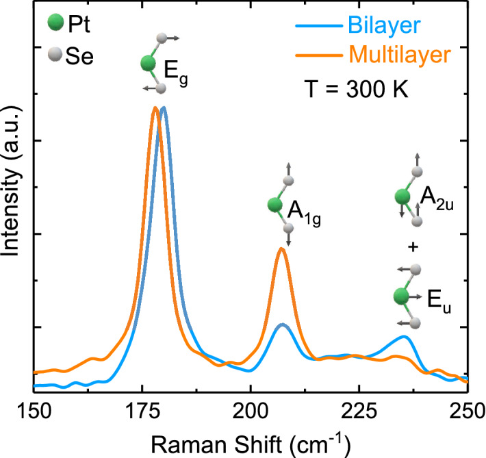
Raman scattering spectra of PtSe2 thin films at room temperature. The inset illustrates vibrational modes of both PtSe2 thin films 50.
Table 2.
Raman phonon modes observed at room temperature for bilayer and multilayer PtSe2 thin films with their corresponding assignments.
| Layer type | ω1 /Eg (cm−1) | ω2/A1g (cm−1) | ω3/LO (cm−1) |
|---|---|---|---|
| Bilayer | 179 | 207 | 235 |
| Multilayer | 178 | 207 | 232 |
In the normalized condition of the intensity of the Eg mode, two phonon modes (Eg and LO) of PtSe2 thin film shifted to lower frequency ranges (from 179 and 235 cm−1 [bilayer] to 178 and 232 cm−1 [multilayer], respectively) with an increase in the number of layers. Unlikely those two phonon modes, the frequency of the A1g mode of bilayer PtSe2 thin film was unchanged when the number of layers increased. This anomalous behavior is consistent with that of PtSe2 thin film growth through molecular beam epitaxy50. Subsequently, we observed that the A1g mode of multilayer PtSe2 thin film exhibited higher intensity than that of bilayer PtSe2 thin film because of stacking-induced structural changes and long-range Coulombic interlayer interactions51. The intensity of the LO mode decreased with an increase in thickness. This behavior could be associated with the enhanced interlayer coupling in multilayer PtSe2 thin film27.
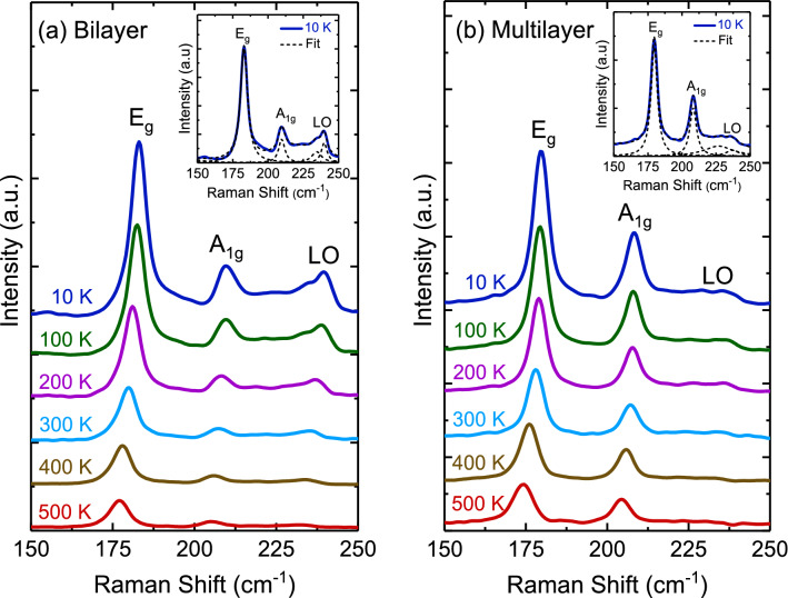
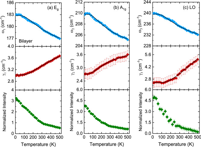
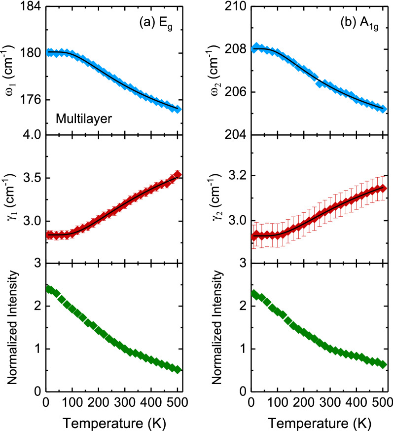
Figure 10 displays the temperature dependence of the Raman scattering spectra of bilayer and multilayer PtSe2 thin films. When the temperature decreased, the peak positions of all phonon modes shifted to higher frequencies, and their resonance linewidth decreased. The Raman scattering spectra exhibited sharp phonon modes at 10 K for both thin films. Four Lorentzian oscillators were used to represent the Raman scattering spectrum at 10 K (inset of Fig. 10), whereas the background was taken to be linear in these fits of the form Aω + B, where A and B are adjustable parameters. Figures 11 and 12 illustrate the frequency, linewidth, and normalized intensity of phonon modes as functions of temperature. The phonon modes changed continuously from temperatures of 500 to 10 K. In a normal anharmonic solid, a decrease in temperature causes an increase in phonon frequency but a decrease in linewidth. Anharmonic interactions are relevant to higher-order terms of atomic vibrations that are beyond traditional harmonic terms. The temperature-dependent phonon frequency and linewidth can be expressed as follows52:
| 3 |
| 4 |
where ω0 is the intrinsic frequency of the optical phonon mode, γ0 is linewidth broadening due to defects, A and B are anharmonic coefficients, and Θ is the Debye temperature. The values of the fitting parameters are summarized in Table 3.
Figure 10.
Temperature-dependent Raman scattering spectra of (a) bilayer and (b) multilayer PtSe2 thin films. The inset displays Raman scattering spectrum with Lorentzian oscillators of bilayer and multilayer PtSe2 thin films at 10 K.
Figure 11.
Temperature dependence of the frequency, linewidth, and normalized intensity of (a) Eg, (b) A1g, and (c) LO modes for bilayer PtSe2 thin film. The thin solid lines indicate the results of the fitting from the anharmonic model by using Eqs. (3) and (4).
Figure 12.
Temperature dependence of the frequency, linewidth, and normalized intensity of (a) Eg and (b) A1g modes for multilayer PtSe2 thin film. The thin solid lines indicate the results of the fitting from the anharmonic model by using Eqs. (3) and (4).
Table 3.
Parameter values obtained from fitting the temperature dependence of phonon frequencies and linewidths according to the anharmonic model using Eqs. (3) and (4).
| Layer type | Mode | ω0 (cm−1) | γ0 (cm−1) | A (cm−1) | B (cm−1) | (K) |
|---|---|---|---|---|---|---|
| Bilayer | Eg | 182.8 | 3.0 | − 6.1 | 0.9 | 382 |
| A1g | 209.8 | 2.6 | − 4.2 | 0.7 | 313 | |
| Multilayer | Eg | 180.1 | 2.8 | − 5.2 | 0.8 | 390 |
| A1g | 208 | 2.9 | − 2.7 | 0.3 | 339 |
Table 3 indicates that the high absolute A values of Eg and A1g modes in bilayer and multilayer PtSe2 thin films revealed a dominant anharmonic interaction between Pt and Se atoms. These large values are crucial for reducing lattice thermal conductivity53. The relatively small absolute B values of Eg and A1g modes in bilayer and multilayer PtSe2 thin films were associated with strong anharmonic phonon–phonon interactions. Thus, anharmonic phonon scattering with three-phonon process (Eqs. 3 and 4) is highly favorable for bilayer and multilayer PtSe2 thin films. At a temperature of 10 K, as depicted in Fig. 10, the LO phonon mode of bilayer PtSe2 thin film exhibited a peak position that split into two-phonon modes (A2u and Eu) at approximately 235 and 239 cm−1. By contrast, multilayer PtSe2 thin film exhibited a broadening peak at approximately 236 cm−1. Moreover, the A2u and Eu phonon modes of bilayer PtSe2 thin film exhibited a blueshift and an increase in intensity in temperature with a decrease in temperature.
Summary
The temperature-dependent optical properties of bilayer and multilayer PtSe2 thin films were investigated through spectroscopic ellipsometry and Raman scattering spectroscopy. Large value of the refractive index (approximately 6.88) in the near-infrared frequency range was obtained for multilayer PtSe2 thin film. The thermo-optic coefficients of bilayer and multilayer PtSe2 thin films were (4.31 ± 0.04) × 10−4/K and (–9.20 ± 0.03) × 10−4/K at a wavelength of 1200 nm. The room-temperature optical absorption spectra revealed that bilayer PtSe2 thin film had an indirect band gap of approximately 0.75 ± 0.01 eV, whereas multilayer PtSe2 thin film exhibited semimetal behavior. The band gap of bilayer PtSe2 thin film increased to 0.83 ± 0.01 eV at 4.5 K. By contrast, multilayer PtSe2 thin film exhibited a band gap energy of approximately 0.04 ± 0.004 eV at 500 K. Moreover, the temperature-dependent phonon frequency and linewidth of Raman-active Eg and A1g modes of both thin films accorded with the predictions of the anharmonic model. These results provide fundamental information regarding PtSe2-based devices for optoelectronic and photonic applications at various temperatures.
Data availability statement
The data that support the findings of this study are available from the corresponding author upon reasonable request.
Supplementary information
Acknowledgements
H.L.L. thanks financial support from the Ministry of Science and Technology of Republic of China under Grants No. MOST 109-2112-M-003-016. W.H.C. thanks financial support from the Ministry of Science and Technology of Republic of China under Grants No. 108-2119-M-009-011-MY3.
Author contributions
H.L.L. conceived the research and was responsible for the experimental design. D.P.G. conducted the experiments. H.Y. and W.H.C. were responsible for the sample preparation. D.P.G. and H.L.L. drafted the paper. All contributing authors have discussed the results and provided the comments regarding the manuscript.
Competing interests
The authors declare no competing interests.
Footnotes
Publisher's note
Springer Nature remains neutral with regard to jurisdictional claims in published maps and institutional affiliations.
Supplementary information
is available for this paper at 10.1038/s41598-020-76036-y.
References
- 1.Duan X, Wang C, Pan A, Yu R, Duan X. Two-dimensional transition metal dichalcogenides as atomically thin semiconductors: opportunities and challenges. Chem. Soc. Rev. 2015;44:8859. doi: 10.1039/C5CS00507H. [DOI] [PubMed] [Google Scholar]
- 2.Manzeli S, Ovchinnikov D, Pasquier D, Yazyev OV, Kis A. 2D transition metal dichalcogenides. Nat. Rev. Mater. 2017;2:17033. doi: 10.1038/natrevmats.2017.33. [DOI] [Google Scholar]
- 3.Roldán R, Silva-Guillén JA, López-Sancho MP, Guinea F, Cappelluti E, Ordejón P. Electronic properties of single-layer and multilayer transition metal dichalcogenides MX2 ( M = Mo, W and X = S, Se) Ann. Phys. 2014;526:347. doi: 10.1002/andp.201400128. [DOI] [Google Scholar]
- 4.Jariwala D, Sangwan VK, Lauhon LJ, Marks TJ, Hersam MC. Emerging device applications for semiconducting two-dimensional transition metal dichalcogenides. ACS Nano. 2014;8:1102. doi: 10.1021/nn500064s. [DOI] [PubMed] [Google Scholar]
- 5.Kolobov AV, Tominaga J. Two-Dimensional Transition-Metal Dichalcogenides. New York: Springer; 2016. [Google Scholar]
- 6.Mak KF, Lee C, Hone J, Shan J, Heinz TF. Atomically thin MoS2: a new direct-gap semiconductor. Phys. Rev. Lett. 2010;105:136805. doi: 10.1103/PhysRevLett.105.136805. [DOI] [PubMed] [Google Scholar]
- 7.Zhao W, Ribeiro RM, Toh M, Carvalho A, Kloc C, Castro Neto AH, Eda G. Origin of indirect optical transitions in few-layer MoS2, WS2, and WSe2. Nano Lett. 2013;13:5627. doi: 10.1021/nl403270k. [DOI] [PubMed] [Google Scholar]
- 8.Liu, H. L., Shen, C. C., Su, S. H., Hsu, C. L., Li, M. Y. & Li, L. J. Optical properties of monolayer transition metal dichalcogenides probed by spectroscopic ellipsometry. Appl. Phys. Lett. 105, (2014).
- 9.Li J, Chen X, Zhang D, Zhou P. Van der Waals heterostructure based field effect transistor application. Crystals. 2017;8:8. doi: 10.3390/cryst8010008. [DOI] [Google Scholar]
- 10.Sangwan VK, Hersam MC. Electronic transport in two-dimensional materials. Annu. Rev. Phys. Chem. 2018;69:299. doi: 10.1146/annurev-physchem-050317-021353. [DOI] [PubMed] [Google Scholar]
- 11.Nguyen HT, Kim TJ, Park HG, Le VL, Nguyen XA, Koo D, Lee C-H, Cuong DD, Hong SC, Kim YD. Temperature dependence of optical properties of monolayer WS2 by spectroscopic ellipsometry. Appl. Surf. Sci. 2020;511:145503. doi: 10.1016/j.apsusc.2020.145503. [DOI] [Google Scholar]
- 12.Choi W, Choudhary N, Han GH, Park J, Akinwande D, Lee YH. Recent development of two-dimensional transition metal dichalcogenides and their applications. Mater. Today. 2017;20:116. doi: 10.1016/j.mattod.2016.10.002. [DOI] [Google Scholar]
- 13.Chen H-Y, Palummo M, Sangalli D, Bernardi M. Theory and ab initio computation of the anisotropic light emission in monolayer transition metal dichalcogenides. Nano Lett. 2018;18:3839. doi: 10.1021/acs.nanolett.8b01114. [DOI] [PubMed] [Google Scholar]
- 14.Choi BK, Kim M, Jung K-H, Kim J, Yu K-S, Chang YJ. Temperature dependence of band gap in MoSe2 grown by molecular beam epitaxy. Nanoscale Res. Lett. 2017;12:492. doi: 10.1186/s11671-017-2266-7. [DOI] [PMC free article] [PubMed] [Google Scholar]
- 15.Huo N, Yang Y, Wu Y-N, Zhang X-G, Pantelides ST, Konstantatos G. High carrier mobility in monolayer CVD-grown MoS2 through phonon suppression. Nanoscale. 2018;10:15071. doi: 10.1039/C8NR04416C. [DOI] [PubMed] [Google Scholar]
- 16.Wang QH, Kalantar-Zadeh K, Kis A, Coleman JN, Strano MS. Electronics and optoelectronics of two-dimensional transition metal dichalcogenides. Nat. Nanotechnol. 2012;7:699. doi: 10.1038/nnano.2012.193. [DOI] [PubMed] [Google Scholar]
- 17.Wu K, Ma H, Gao Y, Hu W, Yang J. Highly-efficient heterojunction solar cells based on two-dimensional tellurene and transition metal dichalcogenides. J. Mater. Chem. A. 2019;7:7430. doi: 10.1039/C9TA00280D. [DOI] [Google Scholar]
- 18.Rawat B, Vinaya MM, Paily R. Transition metal dichalcogenide-based field-effect transistors for analog/mixed-signal applications. IEEE Trans. Electron Devices. 2019;66:2424. doi: 10.1109/TED.2019.2906235. [DOI] [Google Scholar]
- 19.Yang Y, Jang SK, Choi H, Xu J, Lee S. Homogeneous platinum diselenide metal/semiconductor coplanar structure fabricated by selective thickness control. Nanoscale. 2019;11:21068. doi: 10.1039/C9NR07995E. [DOI] [PubMed] [Google Scholar]
- 20.Kandemir A, Akbali B, Kahraman Z, Badalov SV, Ozcan M, Iyikanat F, Sahin H. Structural, electronic and phononic properties of PtSe2: from monolayer to bulk. Semicond. Sci. Technol. 2018;33:085002. doi: 10.1088/1361-6641/aacba2. [DOI] [Google Scholar]
- 21.Shi J, Huan Y, Hong M, Xu R, Yang P, Zhang Z, Zou X, Zhang Y. Chemical vapor deposition grown large-scale atomically thin platinum diselenide with semimetal–semiconductor transition. ACS Nano. 2019;13:8442. doi: 10.1021/acsnano.9b04312. [DOI] [PubMed] [Google Scholar]
- 22.Zhao Y, Qiao J, Yu Z, Yu P, Xu K, Lau SP, Zhou W, Liu Z, Wang X, Ji W, Chai Y. High-electron-mobility and air-stable 2D layered PtSe2 FETs. Adv. Mater. 2017;29:1604230. doi: 10.1002/adma.201604230. [DOI] [PubMed] [Google Scholar]
- 23.Yim C, Lee K, McEvoy N, O’Brien M, Riazimehr S, Berner NC, Cullen CP, Kotakoski J, Meyer JC, Lemme MC, Duesberg GS. High-performance hybrid electronic devices from layered PtSe2 films grown at low temperature. ACS Nano. 2016;10:9550. doi: 10.1021/acsnano.6b04898. [DOI] [PubMed] [Google Scholar]
- 24.Zeng L, Lin S, Lou Z, Yuan H, Long H, Li Y, Lu W, Lau SP, Wu D, Tsang YH. Ultrafast and sensitive photodetector based on a PtSe2/silicon nanowire array heterojunction with a multiband spectral response from 200 to 1550 nm. NPG Asia Mater. 2018;10:352. doi: 10.1038/s41427-018-0035-4. [DOI] [Google Scholar]
- 25.Yuan J, Mu H, Li L, Chen Y, Yu W, Zhang K, Sun B, Lin S, Li S, Bao Q. Few-layer platinum diselenide as a new saturable absorber for ultrafast fiber lasers. ACS Appl. Mater. Interfaces. 2018;10:21534. doi: 10.1021/acsami.8b03045. [DOI] [PubMed] [Google Scholar]
- 26.Wang Y, Li L, Yao W, Song S, Sun JT, Pan J, Ren X, Li C, Okunishi E, Wang Y-Q, Wang E, Shao Y, Zhang YY, Yang H, Schwier EF, Iwasawa H, Shimada K, Taniguchi M, Cheng Z, Zhou S, Du S, Pennycook SJ, Pantelides ST, Gao H-J. Monolayer PtSe2, a new semiconducting transition-metal-dichalcogenide, epitaxially grown by direct selenization of Pt. Nano Lett. 2015;15:4013. doi: 10.1021/acs.nanolett.5b00964. [DOI] [PubMed] [Google Scholar]
- 27.O’Brien M, McEvoy N, Motta C, Zheng J-Y, Berner NC, Kotakoski J, Elibol K, Pennycook TJ, Meyer JC, Yim C, Abid M, Hallam T, Donegan JF, Sanvito S, Duesberg GS. Raman characterization of platinum diselenide thin films. 2D Mater. 2016;3:021004. doi: 10.1088/2053-1583/3/2/021004. [DOI] [Google Scholar]
- 28.Yu X, Yu P, Wu D, Singh B, Zeng Q, Lin H, Zhou W, Lin J, Suenaga K, Liu Z, Wang QJ. Atomically thin noble metal dichalcogenide: a broadband mid-infrared semiconductor. Nat. Commun. 2018;9:1545. doi: 10.1038/s41467-018-03935-0. [DOI] [PMC free article] [PubMed] [Google Scholar]
- 29.Xie J, Zhang D, Yan X-Q, Ren M, Zhao X, Liu F, Sun R, Li X, Li Z, Chen S, Liu Z-B, Tian J-G. Optical properties of chemical vapor deposition-grown PtSe2 characterized by spectroscopic ellipsometry. 2D Mater. 2019;6:035011. doi: 10.1088/2053-1583/ab1490. [DOI] [Google Scholar]
- 30.Yeh, H., Wu, Y., Yeh, T., Li, C., Chou, Y., Li, M., Chou, Y., Luo, C. W., Li, L. & Chang, W. H. Scalable fabrication of PtSe2 metal-semiconductor lateral junctions via local layer engineering (private communication).
- 31.Chen HW, Chen Y-W, Kuo J-L, Lai YC, Chou FC, Du CH, Liu HL. Spin-charge-lattice coupling in YBaCuFeO5: Optical properties and first-principles calculations. Sci. Rep. 2019;9:3223. doi: 10.1038/s41598-019-39031-6. [DOI] [PMC free article] [PubMed] [Google Scholar]
- 32.Liu HL, Yang T, Chen JH, Chen HW, Guo HH, Saito R, Li MY, Li LJ. Temperature-dependent optical constants of monolayer MoS2, MoSe2, WS2, and WSe2: spectroscopic ellipsometry and first-principles calculations. Sci. Rep. 2020;10:15282. doi: 10.1038/s41598-020-71808-y. [DOI] [PMC free article] [PubMed] [Google Scholar]
- 33.Hashmi S. Reference Module in Materials Science and Materials Engineering. Oxford: Elsevier; 2016. [Google Scholar]
- 34.Hecht E. Optics. London: Addison Wesley; 2002. [Google Scholar]
- 35.Born M, Wolf E. Principles of Optics - 7th (Expanded) Edition. Cambridge: Cambridge University Press; 1999. [Google Scholar]
- 36.Soref R. The past, present, and future of silicon photonics. IEEE J. Sel. Top. Quantum Electron. 2006;12:1678. doi: 10.1109/JSTQE.2006.883151. [DOI] [Google Scholar]
- 37.Ma M, Mont FW, Poxson DJ, Cho J, Schubert EF, Welser RE, Sood AK. Enhancement of photovoltaic cell response due to high-refractive-index encapsulants. J. Appl. Phys. 2010;108:043102. doi: 10.1063/1.3466980. [DOI] [Google Scholar]
- 38.Komma J, Schwarz C, Hofmann G, Heinert D, Nawrodt R. Thermo-optic coefficient of silicon at 1550 nm and cryogenic temperatures. Appl. Phys. Lett. 2012;101:041905. doi: 10.1063/1.4738989. [DOI] [Google Scholar]
- 39.Wiechmann S, Müller J. Thermo-optic properties of TiO2, Ta2O5 and Al2O3 thin films for integrated optics on silicon. Thin Solid Films. 2009;517:6847. doi: 10.1016/j.tsf.2009.05.040. [DOI] [Google Scholar]
- 40.Sajjad M, Singh N, Schwingenschlögl U. Strongly bound excitons in monolayer PtS2 and PtSe2. Appl. Phys. Lett. 2018;112:043101. doi: 10.1063/1.5010881. [DOI] [Google Scholar]
- 41.Pankove JI. Optical Proccesses in Semiconductors. New York: Springer; 1971. [Google Scholar]
- 42.Zhao X, Liu F, Liu D, Yan X-Q, Huo C, Hui W, Xie J, Ye Q, Guo C, Yao Y, Liu Z-B, Tian J-G. Thickness-dependent ultrafast nonlinear absorption properties of PtSe2 films with both semiconducting and semimetallic phases. Appl. Phys. Lett. 2019;115:263102. doi: 10.1063/1.5135375. [DOI] [Google Scholar]
- 43.Chen X, Zhang S, Wang L, Huang Y-F, Liu H, Huang J, Dong N, Liu W, Kislyakov IM, Nunzi JM, Zhang L, Wang J. Direct observation of interlayer coherent acoustic phonon dynamics in bilayer and few-layer PtSe2. Photonics Res. 2019;7:1416. doi: 10.1364/PRJ.7.001416. [DOI] [Google Scholar]
- 44.O’Donnell KP, Chen X. Temperature dependence of semiconductor band gaps. Appl. Phys. Lett. 1991;58:2924. doi: 10.1063/1.104723. [DOI] [Google Scholar]
- 45.Pässler R, Griebl E, Riepl H, Lautner G, Bauer S, Preis H, Gebhardt W, Buda B, As DJ, Schikora D, Lischka K, Papagelis K, Ves S. Temperature dependence of exciton peak energies in ZnS, ZnSe, and ZnTe epitaxial films. J. Appl. Phys. 1999;86:4403. doi: 10.1063/1.371378. [DOI] [Google Scholar]
- 46.Pejova B, Abay B, Bineva I. Temperature dependence of the band-gap energy and sub-band-gap absorption tails in strongly quantized ZnSe nanocrystals deposited as thin films. J. Phys. Chem. C. 2010;114:15280. doi: 10.1021/jp102773z. [DOI] [Google Scholar]
- 47.Gibbs ZM, Kim H, Wang H, White RL, Drymiotis F, Kaviany M, Snyder GJ. Temperature dependence band gap in PbX (X = S, Se, Te) Appl. Phys. Lett. 2013;103:262109. doi: 10.1063/1.4858195. [DOI] [Google Scholar]
- 48.Zhao K, Huang F, Dai CM, Li W, Chen SY, Jiang K, Huang YP, Hu Z, Chu J. Temperature dependence of phonon modes, optical constants, and optical band gap in two-dimensional ReS2 films. J. Phys. Chem. C. 2018;122:29464. doi: 10.1021/acs.jpcc.8b08693. [DOI] [Google Scholar]
- 49.Cingolani A, Ferrara M, Lugarà M, Lévy F. The Raman spectra of CdI2. Solid State Commun. 1984;50:911. doi: 10.1016/0038-1098(84)90747-6. [DOI] [Google Scholar]
- 50.Yan M, Wang E, Zhou X, Zhang G, Zhang H, Zhang K, Yao W, Lu N, Yang S, Wu S, Yoshikawa T, Miyamoto K, Okuda T, Wu Y, Yu P, Duan W, Zhou S. High quality atomically thin PtSe2 films grown by molecular beam epitaxy. 2D Mater. 2017;4:1. doi: 10.1088/2053-1583/aa8919. [DOI] [Google Scholar]
- 51.Lee C, Yan H, Brus LE, Heinz TF, Hone J, Ryu S. Anomalous lattice vibrations of single- and few-layer MoS2. ACS Nano. 2010;4:2695. doi: 10.1021/nn1003937. [DOI] [PubMed] [Google Scholar]
- 52.Balkanski M, Wallis RF, Haro E. Anharmonic effects in light scattering due to optical phonons in silicon. Phys. Rev. B. 1983;28:1928. doi: 10.1103/PhysRevB.28.1928. [DOI] [Google Scholar]
- 53.Chen L-C, Cao Z-Y, Yu H, Jiang B-B, Su L, Shi X, Chen L-D, Chen X-J. Phonon anharmonicity in thermoelectric palladium sulfide by Raman spectroscopy. Appl. Phys. Lett. 2018;113:022105. doi: 10.1063/1.5041973. [DOI] [Google Scholar]
Associated Data
This section collects any data citations, data availability statements, or supplementary materials included in this article.
Supplementary Materials
Data Availability Statement
The data that support the findings of this study are available from the corresponding author upon reasonable request.


