Abstract
The combination of metal-assisted chemical etching (MACE) with colloidal lithography has emerged as a simple and cost-effective approach to nanostructure silicon. It is especially efficient at synthesizing Si micro- and nanowire arrays using a catalytic metal mesh, which sinks into the silicon substrate during the etching process. The approach provides a precise control over the array geometry, without requiring expensive nanopatterning techniques. Although MACE is a high-throughput solution-based approach, achieving large-scale homogeneity can be challenging because of the instability of the metal catalyst when the experimental parameters are not set appropriately. Such instabilities can lead to metal film fracture, significantly damaging the substrate and thus compromising the nanowire array quality. Here, we report on the critical parameters that influence the stability of the metal catalyst layer for achieving large-scale homogeneous MACE: etchant composition, metal film thickness, adhesion layer thickness, nanowire diameter and pitch, metal film coverage, Si/Au/etchant interface length, and crystalline quality of the colloidal template (grain size and defects). Our results investigate the origin of the catalyst film fracture and reveal that MACE experiments should be optimized for each Si wire array geometry by keeping the etch rate below a certain threshold. We show that the Si/Au/etchant interface length also affects the etch rate and should thus be considered when optimizing the MACE experimental parameters. Finally, our results demonstrate that colloidal templates with small grain sizes (i.e., <100 μm2) can yield significant problems during the pattern transfer because of a high density of defects at the grain boundaries that negatively affects the metal film stability. As such, this work provides guidelines for the large-scale synthesis of Si micro- and nanowire arrays via MACE, relevant for both new and experienced researchers working with MACE.
Introduction
Micro- and nanostructuring silicon is a crucial process for the fabrication and development of transistors, micro-electromechanical systems, optical sensors, metamaterials, and Si-based batteries.1−4 Vertically aligned silicon nanowire (VA-SiNW) arrays are a particularly interesting class of nanostructured silicon because of their strong and tunable interaction with light that can arise from wave-guiding,5,6 Mie resonance excitation,7 diffractive effects,8 and near-field coupling.9 Controlling these effects via the structural properties of the VA-SiNWs leads to tunable light scattering,7 absorption,5,6 and reflection.10 As such, they have shown great promise for the next generation of photovoltaic,11−13 photocatalytic,14−16 and sensing6,7,9,17 devices.
Historically, VA-SiNW arrays have been first prepared via vapor–liquid–solid (VLS) synthesis.18−20 At the time, VLS afforded a versatile route to prepare single-crystal Si nanowires. It was later found that the conventional metal catalyst used for VLS, gold, diffuses within the nanowires during the synthesis and acts as trap levels, significantly increasing Shockley–Read–Hall recombination and affecting the nanowire electrical performance.21 As such, most VLS-grown Si nanowires are not CMOS-compatible. Dispersed Si nanowires can be prepared via the solution–liquid–solid (SLS) method, which has the advantage of being low cost and has potential for large-scale production.22,23 However, the preparation of highly ordered VA-SiNW arrays via SLS remains to be seen. The most common ways to prepare arrays of high aspect ratio structures are reactive-ion etching and deep-reactive-ion etching.24 Unfortunately, these methods yield surface damages and require expensive infrastructures that are not always available.25 Metal-assisted chemical etching (MACE) on the other hand is a cost-effective, solution-based, and high-throughput technique to micro- and nanostructure silicon with high structure fidelity and purity.5,20,26−40 It involves a nanostructured metal catalyst layer, an oxidant, and hydrofluoric acid (HF).26−28,41 The oxidizing agent, usually H2O2, is preferentially reduced at the surface of the metal catalyst, generating holes (eq 1) that are injected through the metal/silicon Schottky barrier, which, in the presence of HF, oxidizes silicon into a soluble product and generate hydrogen gas as a byproduct (eq 2).28
| 1 |
| 2 |
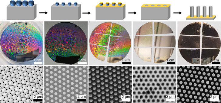
where h+ is a hole. As a result, the silicon in contact with the metal catalyst dissolves, leading to a highly anisotropic etching: during MACE, isolated metal catalyst particles sink into the silicon, forming vertical and straight pores,26 while continuous metal nanomeshes can be used to produce VA-SiNW arrays.27,29,30,34,35 Colloidal lithography, based on self-assembled colloidal particles used as a mask, has emerged as a low-cost, versatile, and simple approach to synthesize such metal nanomeshes with full control over diameter and pitch.42−44 Its use in combination with MACE offers great promise for the large-scale and cost-effective production of silicon micro- and nanowire arrays (Figure 1).26,27,33,34 Because colloidal lithography can be used to prepare metal nanomeshes with controlled array parameters and hole morphologies, it can potentially be used to prepare a variety of VA-SiNW arrays via MACE.45−47 For example, under specific plasma etching conditions, the spherical shape of the colloidal particles can be altered to produce particles with a hexagonal cross-section which, after MACE, produce Si nanowires with a hexagonal morphology.34 Furthermore, the colloidal mask pattern can be controlled by the deposition conditions,46,47 while binary colloidal masks made with two different sized colloidal particles can be used to prepare arrays of Si nanowires with two different diameters via MACE.45,48
Figure 1.
Synthesis of silicon nanowire arrays via colloidal lithography and MACE. Top row: Schematics showing the successive synthetic steps. Middle row: Photographs of 2″ Si wafers during the process. Bottom row: Secondary electron SEM images. A monolayer of PS colloidal particles (d = 1100 nm) (in blue) is self-assembled on the surface of the silicon wafer (in gray). The size of the spheres is reduced using oxygen plasma etching (d = 780 nm). A gold film is sputtered onto the monolayer mask, which, after lift-off, yields a continuous gold nanomesh. The gold film sinks into the silicon during MACE in HF/H2O2, yielding well-defined silicon nanowire arrays.
Although MACE is a simple wet chemical etching technique, performing it appropriately is not straightforward: when the MACE parameters are not optimized, the metal etching mask can bend, break, and delaminate during etching, leading to macroscopic areas where the substrate is not uniformly etched, and can even be irreversibly damaged. The remarkable etching anisotropy obtained via MACE is attributed to attractive van der Waals interactions which forces the metal catalyst to stay in contact with the silicon during etching.31,32 However, an increase in the Au–Si distance during etching (which increases for increasing concentrations of H2O2) decreases the van der Waals attractive forces,31 which can lead to gold film delamination.33 The use of an adhesion layer such as titanium or aluminum-doped zinc oxide (AZO) can circumvent this problem by improving the film stability (Figure 2).5,33,34,49 Because MACE depends on both hole injection and mass transport of the reactants and reaction products in-and-out of the Au–Si interface region, the metal mesh morphology influences the MACE process and resulting product geometry. For example, nanoporous metal meshes facilitate mass transport but yield additional unwanted thin silicon nanowires at the positions of these nanopores.26,35−37 In addition to the metal film properties, the silicon-doping type and density also affect the etching anisotropy because of band-bending at the metal/Si Schottky junction that controls hole localization at the metal/silicon interface.28 Finally, high etch rates have been reported to destabilize isolated metal nanoparticle catalysts and decrease etching anisotropy, although the origin of the destabilization events is still unclear.32
Figure 2.
MACE with and without the adhesion layer. (a,b) Top row: Large-scale photographs. Bottom row: Secondary electron SEM images. (a) Substrate after MACE without the adhesion layer. Inhomogeneous etching due to the bad contact between the Si and Au leads to film delamination or no etching in large areas. (b) Utilization of an aluminum-doped zinc oxide (AZO) adhesion layer improves the contact and homogeneous etching. (c) Etch rate as a function of wire diameter for three different AZO thicknesses: the AZO layer was deposited during 1 s at 75 W (black symbols), 150 W (blue symbols), and 400 W (green symbols). The SiNW length and etch rate decrease for thicker adhesion layers. The lines are linear fits. Pitch: 590 nm; Au: 200 s 40 mA; MACE etchant composition 10:1:10 HF/H2O2/H2O etched during 7 min. Samples showing regions where the gold film was fractured are shown as triangles. Samples with a stable flat gold film are shown as squares.
Because inhomogeneities in nanowire crystallinity, length, diameter, and density can be detrimental to the array properties at the macroscale,5,16 identifying the parameters that affect the etching uniformity is crucial to synthesize arrays with homogeneous dimensions and uniform properties. Here, we provide a coherent description of the experimental details that are required to form well-ordered VA-SiNW arrays, along with reliable recipes, clear guidelines, and troubleshooting guides to optimize synthesis conditions. We report that the metal catalyst film stability is crucial and depends on many experimental factors. In particular, we show that the etch rate is strongly influenced by the array dimensions (wire diameter and array density) and needs to be lowered below a certain threshold to avoid film fracture and delamination. Notably, the etch rate depends on both the Au coverage and the Au/Si/etchant interface length, while the metal pattern uniformity (i.e., array grain size and defect density) strongly affects the catalyst film stability and thus etching homogeneity.
Experimental Methods
Synthesis of the VA-SiNW Arrays
Large-scale homogeneous silicon micro- and nanowire arrays were synthesized using colloidal lithography and MACE, as previously reported from our group (Figure 1).5,34,38,49 Colloidal lithography involves the self-assembly of colloidal spheres, usually made of polystyrene (PS), into a monolayer that is transferred onto an arbitrary substrate. Plasma etching is used to shrink the particles to obtain hexagonally non-close-packed particle arrays.42 After gold-sputtering deposition and lift-off, a gold nanomesh is formed, which is then used as an etching mask for MACE. The array pitch, SiNW diameter, and length depend on the original sphere diameter, the final PS particle size after plasma etching, and the MACE duration, respectively. Colloidal sphere monolayers were obtained via self-assembly at the water–air interface (PS spheres with initial diameters d = 590 and d = 1100 nm, Figure S1)42,50 and by spin-coating (d = 1500 nm).34 Self-assembly at the water–air interface can be used to produce large-scale, well-ordered colloidal monolayers with large grain sizes, while spin-coating under our experimental conditions consistently yielded highly defective arrays with some regions that were either uncovered or consisted of sphere multilayers (Figure S2). Colloidal templates based on the SiO2 core-PNiPam shell [PNiPAm: poly(N-isopropylacrylamide)] particles were prepared with a Langmuir–Blodgett (LB) trough, yielding high-quality monolayers, which, after etching the polymeric shell via oxygen plasma, yielded non-close-packed hexagonal array of SiO2 spheres with controllable lattice spacings.8,38,51 Prior to gold-sputtering, a thin adhesion layer of AZO was sputtered on each silicon substrate to establish a stable contact between the gold film and the silicon.5,33,34,38,49 After metal deposition, the colloidal particles (either PS or SiO2) were removed using an adhesive tape (Scotch Magic tape) (Figure S3). MACE was performed by immersing the substrates in an aqueous HF/H2O2 solution (typically prepared with a HF/H2O2/H2O volumic ratio of 10:0.75:10) for the desired duration (Figure S4). When a high H2O2 concentration is used, porous silicon can form preferentially at the top of the wires, which oxidizes readily in air.52 After an HF cleaning step, this can lead to tapered and even conical Si nanowires.52 In our experience, an HF post-treatment is an efficient way to quantify the amount of porous silicon formed during MACE. Thus, all wire arrays were cleaned in HF right after MACE. Some wires synthesized for this work had some degree of tapering, up to ca. 10%, that is, with a diameter at the top that is 10% smaller than the diameter at the bottom. However, we did not observe more significant tapering of the wires produced under the experimental conditions reported in this manuscript. The complete procedures and involved materials are described in detail in the Supporting Information and in Figures S1–-S4.
Results and Discussion
Based on our extensive expertise in MACE,5,34,38,49 we identified the following important parameters for the reliable synthesis of VA-SiNW arrays: etchant composition, metal film and adhesion layer thicknesses, nanowire diameter and pitch, metal film coverage, Si/Au/etchant interface length, and quality and grain size of the colloidal template. We systematically vary these parameters to show their influence on the etch rate and the resulting array homogeneity (i.e., metal film stability).
Adhesion Layer
Without the AZO adhesion layer, the gold film either does not etch through the substrate properly or delaminates after the tape removal and during MACE, while the presence of an AZO layer leads to homogeneous etching of the silicon substrates (Figure 2). Interestingly, we found that the etch rate can be precisely controlled with the AZO thickness: thicker AZO layers lead to lower etch rates (Figure 2c). This might be due to the increased resistance and charge recombination within the AZO layer.
Etchant Composition
At a sufficiently high HF concentration, hole injection (i.e., silicon oxidation) is the rate-limiting step.28,31,32,39 Under our MACE conditions (where the HF/H2O2/H2O composition was varied from 10:0.5:10 to 10:2:10), varying the amount of H2O2 was an efficient way to adjust the etch rate up to a factor of 10 (Figure S5). This was used to slow down etching and improve film stability when required.
Metal Film Thickness
A sufficiently thick metal film is required to obtain a continuous and stable gold film. Above etch rates of ca. 0.4 μm/min, thin gold films (i.e., sputtering duration ≤100 s) are considerably damaged with many signs of film fracture during MACE, while thicker gold films (i.e., sputtering duration ≥150 s with a Au film thickness >20 nm) remained mostly horizontal (Figure S6). Once the film breaks, the remaining gold particles etch in a random fashion, leading to undefined morphologies (compare Figure S6c,e). Additionally, discontinuous porous gold films, such as the ones obtained via thermal evaporation of 3 nm Ti and 20 nm Au (Figure S6a), can lead to the formation of unwanted thin nanowires in the flat metal film regions35,37 and should thus be avoided. Therefore, the metal film should be thick enough to be continuous and provide good mechanical stability during MACE.
Etch Rate and the Origin of the Au Film Bending and Fracture
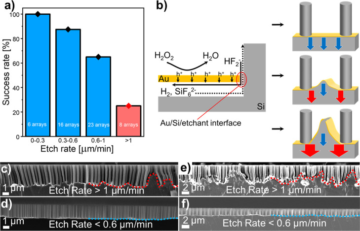
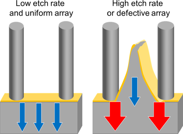
Our experiments revealed a significant influence of the etch rate on the metal film stability and homogeneity of the SiNW arrays synthesized via MACE. The etch rate corresponds to the vertical etch rate; it is equal to the nanowire length [obtained from several cross-sectional scanning electron microscopy (SEM) images] divided by the etching duration. Figure 3 integrates the results of 53 MACE experiments, performed on substrates prepared with a similar Au film thickness but different colloidal particle deposition methods, array geometries, etchant compositions, and AZO thicknesses. Although all these parameters affect the MACE results, a general tendency can be seen from the comparison: the lower the etch rate, the more stable the metal film, and the higher the sample homogeneity (Figure 3a). Typically, low etch rates (below 0.6 μm/min under these MACE conditions) delivered homogeneous results for all pitches, as shown by the presence of a flat horizontal gold film after MACE in more than 85% of the samples produced (Figure 3a,d,f). Interestingly, this is similar to the observations of Vogt et al. who reported 0.7 μm/min as an optimum etch rate for other silicon nanostructures synthesized via MACE.40 At high etch rates (above 1 μm/min under these MACE conditions), the amount of samples that are etched properly reduced to ca. 25%, with many samples showing clear signs of gold film bending and sometimes fracture. These defects in the film in turn prevent the formation of homogeneous Si wire arrays over large areas (Figure 3a,c,e). The gold nanomeshes prepared in this work were nonporous and continuous and are different from the nanoporous metal films used by some groups to perform MACE.28,37 For such continuous metal films, mass transport plays a crucial role:31,35,37,39 under high hole injection (i.e., high H2O2 concentrations), the silicon at the Au/silicon/etchant interface is etched faster than the silicon without direct access to the etchant solution because of mass-transport limitations of H2, HF2–, and SiF62– under the metal film (Figure 3b). When the difference in the etch rate between these two regions reaches a certain threshold (depicted as red and blue arrows on Figure 3b), the gold film starts to buckle and ultimately break under the mechanical stress: the metal film fracture originates from nonhomogeneous etch rates across the substrate because of uneven mass transport.
Figure 3.
Influence of the etch rate on the successful synthesis of VA-SiNW arrays via MACE, based on 53 different MACE experiments performed on substrates prepared with a similar Au film thickness but different colloidal particle deposition methods, array geometries, etchant compositions, and AZO thicknesses. (a) Percentage of successful MACE experiments as a function of etch rate. The total numbers of samples etched within an etch rate range are written in white on each bar. A successful MACE experiment refers to samples with a well-defined flat horizontal gold film after MACE, while failed samples correspond to substrates where there is a significant buckling or fracture of the gold film. (b) Schematic illustration of the film fracture origin. Left: Mass-transport limitation due to the diffusion of HF2–, H2, and SiF62– under the gold film. Right: The blue arrows represent low-etch rate regions, while the red arrows represent regions where the etch rate is higher. Top: No mass-transport limitation (low hole injection and etch rate); Center: Some mass-transport limitation leads to a larger etch rate at the Au/Si/etchant interface and buckling of the gold film (moderate hole injection and etch rate); and Bottom: Significant mass-transport limitation leads to spatially inhomogeneous etch rates and gold film fracture (high hole injection and etch rate). (c–f) Secondary electron cross-sectional SEM images of typical arrays synthesized with high etch rates (i.e., >1 μm/min), leading to the buckling and in some cases, fracture of the gold film (c,e), and at low etch rates (i.e. <0.6 μm/min), yielding homogeneous etching, indicated by a flat gold film (d,f). (c,d) Pitch: = 590 nm. (e,f) Pitch: 1100 nm.
Nanowire Diameter
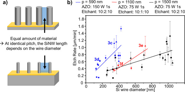
In the following section, we demonstrate that the etching rate is not only affected by the etching solution or the adhesion layer, which can be adjusted individually for each sample, but also by the geometry of the catalyst mask. Indeed, the MACE rate is strongly influenced by the wire diameter (Figure 4) because the etch rate directly depends on the amount of silicon to be etched, which scales with the Au coverage of the nanohole film used as a template. Thus, under identical pitch and MACE conditions, the etch rate decreases for arrays with higher Au coverages, corresponding to arrays with smaller wire diameters (Figure 4b), synthesized using smaller PS particles during the colloidal lithography (i.e., the PS particles were etched for longer times during the oxygen plasma etching step). This is schematically depicted in Figure 4a showing the relative wire length of arrays with identical pitch but different wire diameters; the blue rectangles have the same areas and correspond to the same amount of dissolved silicon. Indeed, arrays with smaller wire diameters are etched much slower for all three pitches considered here (i.e., 1500, 1100, and 590 nm, Figure 4b). For example, for the pitch p = 590 nm, arrays with d = 140 nm etch at ca. 0.4 μm/min, while arrays with d = 380 nm etch at ca. 1.2 μm/min. This is especially relevant for researchers interested in diameter-dependent properties, who often synthesize the catalytic nanomeshes via colloidal lithography using a specific PS particle template (i.e., fixed particle diameter and thus fixed array pitch) and shrinking it via oxygen plasma to access different wire diameters.
Figure 4.
Influence of the nanowire diameter on the etch rate and gold film stability. (a) Scheme depicting the influence of the wire diameter on the etch rate and wire length. At identical pitches, arrays with smaller wire diameter require a higher amount of silicon to be etched to obtain the same wire length, leading to a lower vertical etch rate and shorter nanowires for the same duration. This is represented by the blue rectangles, which have the same area. (b) Vertical etch rate as a function of the Si wire diameter for different pitches. Arrays with larger diameters (same pitch) are etched faster under the same conditions. The graph aggregate data obtained on 35 arrays. Three different pitches were used: black symbols: 1500 nm, red symbols: 1100 nm, and blue symbols: 590 nm. Samples with a buckled gold film are shown as triangles. Samples with a stable flat gold film are shown as squares. The lines are linear fits. The wire diameters ranged from 120 to 1050 nm. Au-sputtering conditions: 200 s at 40 mA for all substrates. The samples corresponding to the SEM images shown in Figure 3c–f are indicated.
The negative influence of large etch rates on substrate uniformity is seen by a larger standard deviation in the wire length observed for samples etched fast, leading to a defective gold film (shown with triangle symbols), compared to samples etched slower, leading to an intact gold film (square symbols). Because etching homogeneity strongly depends on the etch rate (Figures 3 and 4), we recommend to adjust the adhesion layer thickness or the etchant composition to reach an appropriate etch rate whenever arrays with different dimensions are synthesized. For this reason, although the Au film thickness was the same for all the samples shown in Figure 4, both the AZO thickness (Figure 2) and the etchant composition (Figure S5) were adjusted for each pitch to keep the etch rate relatively low.
Au Coverage, Nanowire Pitch, and Au/Si/Etchant Interface Length
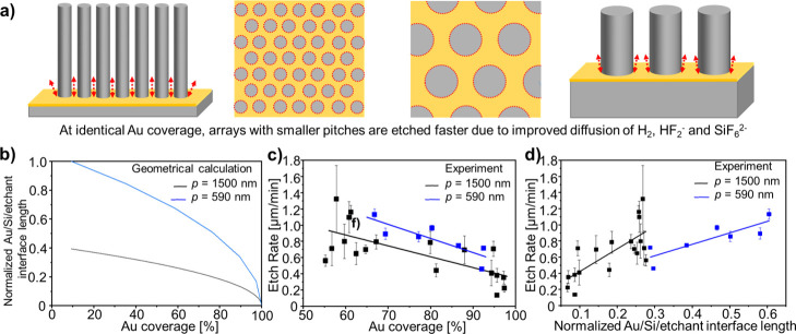
In Figure 5, we show the influence of Au coverage in the nanomesh array on the etch rates for arrays with pitches of 590 and 1500 nm and Au coverages ranging from ca. 55 to 97%, adjusted by the diameter of the colloidal particles in the non-close-packed monolayer used as a mask. All arrays were prepared and etched under the same MACE conditions (i.e., same AZO/Au film thicknesses and etchant composition). As schematically illustrated, the gold coverage influences the amount of silicon to be etched but also affects the Au/Si/etchant interface length (Figure 5a,b). The etch rate decreases for higher Au coverages because of the larger amount of silicon to be etched. Additionally, at identical gold coverages, a change in the etch rate is observed for arrays with a different pitch. Arrays with a 590 nm pitch are etched faster by ca. 0.2–0.3 μm/min than arrays with a 1500 nm pitch (Figure 5c, comparing the blue symbols to the black symbols, respectively). This is verified across all gold coverages investigated. We attribute this to mass-transport limitations of the reactants and reaction products during MACE. Mass transport and thus etching occur faster for longer Au/Si/etchant interfaces (shown as the red dotted circles in Figure 5a). At identical Au coverages, this corresponds to arrays with smaller pitches (Figure 5b,c). At a similar Au/Si/etchant interface length, the etch rate is larger for the largest pitch because of the correspondingly much lower Au coverage (Figure 5b,d). To our knowledge, the influence of the Au/Si/etchant interface length on the etch rate was never reported before and as such, needs to be considered when preparing arrays with different pitches but identical gold coverages.
Figure 5.
Influence of Au coverage, nanowire pitch, and Au/Si/etchant interface length on the etch rate. (a) Scheme illustrating the influence of the Au/Si/etchant interface (dotted red line) and pitch on the etch rate. Both arrays represented have the same Au coverage (i.e., ∼60%) but different diameters and pitches. Left: Corresponds to p = 590 nm and d = 390 nm; Right: Corresponds to p = 1500 nm and d = 1000 nm. Smaller pitches lead to a larger Au/Si/etchant interface available for the diffusion of products and educts, which increases the etch rate. (b) Calculated normalized Au/Si/etchant interface length as a function of the Au coverage for p = 590 nm (blue line) and p = 1500 nm (black line). (c,d) Etch rate as a function of gold coverage (c) and Au/Si/etchant interface length per surface area (d). Blue squares and line: 590 nm pitch; Black squares and line: 1500 nm pitch. Both straight lines correspond to a linear fit. All substrates had an adhesion layer of AZO (75 W 1 s) and gold (40 mA 200 s) and were etched in 10:2:10 HF/H2O2/H2O. (c) 590 nm arrays show a higher etch rates for identical gold coverage. (d) For both pitches, an increase in the etch rate is observed when the Au/Si/etchant interface length increases. At an identical interface length, the etch rate is higher for the 1500 nm pitch because of its much lower gold coverage compared to arrays with a 590 nm pitch.
Colloidal Template Defects
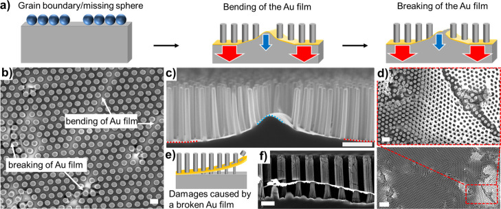
In the previous section, we demonstrated that the etch rate is strongly affected by the geometry of the etching mask and that unfavorable MACE conditions can lead to local fractures of the gold film, which can significantly reduce the homogeneity of the SiNW arrays produced. After carefully reviewing the results of our MACE experiments, we found out that MACE can be very sensitive to local changes in the array geometry, which depend on the quality of the colloidal mask used to fabricate the gold nanohole array that serves as the pattern for the etching process (Figure 6). The colloidal crystal templates used for MACE are polycrystalline and thus show typical crystallographic defects such as vacancies (missing spheres) and grain boundaries (Figure S2). At these defects, the local distance between the spheres increases compared to the average distance found inside the crystalline grain. This increase in distance, in turn, leads locally to higher mass-transport limitations (i.e., lower Au/Si/etchant interface length) and to a higher local Au coverage, corresponding to a larger amount of silicon to etch, both of which locally decreases the etch rate (Figures 4 and 5). This can cause the gold film to bend (Figure 6c). In cases where the local difference in the etch rate is too large, this leads to the fracture of the gold film (Figure 6d). The areas where the gold film is higher and bent can be clearly identified because of their higher brightness in the top-view secondary electron SEM images (Figure 6b). The fracture of the gold film seen in Figure 6d leads to significant damages at the grain boundaries only, while the grain regions remain mostly homogeneous because of their well-defined pitch that provides a constant gold coverage and afford a homogeneous etch rate across the grain. When the gold film breaks, it can delaminate, bend further, and move (Figure 6d), eventually etching parts of the existing wires (Figure 6e,f) and damaging the substrate.
Figure 6.
Influence of the colloidal template defects on substrate uniformity. (a) Schematic illustration explaining the origin of gold film bending and breaking. Defects from the self-assembly process lead to locally slower etch rates (blue arrows). When the local differences in the etch rate are too strong (red vs blue arrows), the gold film bends and finally breaks. (b) Secondary electron SEM image, where the bending and breaking regions can be identified by their higher brightness in regions with missing spheres or at the grain boundaries. Etch rate = 0.23 μm/min. Scale bar: 1 μm. (c) Secondary electron cross-sectional SEM image showing the bending of the gold film in a grain boundary. Scale bar: 1 μm. The blue and red dotted lines highlight the regions of low and high etch rates, respectively. (d) Secondary electron SEM images showing the origin of the damages at the grain boundaries. Etch rate = 0.24 μm/min. Scale bar, top: 2 μm; bottom: 10 μm. (e) Scheme describing the etching of existing Si wires by a fractured gold film. (f) Cross-sectional SEM image that illustrates the situation drawn in e. Scale bar: 1 μm.
Colloidal Template Grain Size
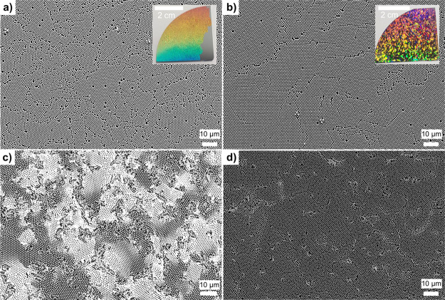
Because failures during MACE depend on the etch rate and the local geometry, the quality of the self-assembled colloidal monolayer used to fabricate the nanohole array is crucial. Large grains support homogeneous etching, while the metal film within small grains can break and be damaged more easily. Figure 7 shows two substrates prepared via self-assembly at the air–water interface with a moderate and a high degree of crystallinity. The highly crystalline template was prepared using a well-purified PS particle dispersion, known to affect the quality of the self-assembled monolayer.50 The difference in grain size can be seen by the naked eye because of the vivid structural colors arising from grating diffraction at ordered domains of the monolayer (insets in Figure 7a,b).8 Although both substrates had similar geometries (p = 1100 nm; d = 710 nm) and were etched with similar etch rates (∼0.25 μm/min), the substrate with a lower degree of order (i.e., smaller grain size, with many grains <100 μm2) was severely damaged (Figure 7a,c). On such substrates, the gold film bends and breaks simultaneously in multiple areas, which can lead to film delamination, causing significant damages to the substrate. On the other hand, a higher degree of order (i.e., larger grain sizes) prevents film delamination and leads to successful MACE. This suggests that a small local density of defects can be compensated by small movements and slight bending of the gold film, ultimately leading to homogeneous MACE. Thus, it is crucial to prepare colloidal templates with the largest grain size possible.
Figure 7.
Influence of grain size and quality of the colloidal monolayer mask on substrate uniformity. (a,b) PS sphere monolayer after self-assembly on silicon (d = 1100 nm). The insets show large-scale photographs. (c,d) SiNW arrays after MACE. (a,c) Substrate with a low degree of order (small grain sizes) led to a destroyed substrate after MACE. p = 1100 nm; d = 713 ± 35 nm; etch rate = 0.24 μm/min; etched during 15 min. (b,d) Substrate with a high degree of order (large grain sizes) led to more homogeneous MACE. p = 1100 nm; d = 709 ± 25 nm; etch rate = 0.28 μm/min; etched during 20 min.
Conditions to Obtain Large-Scale Homogeneity via MACE
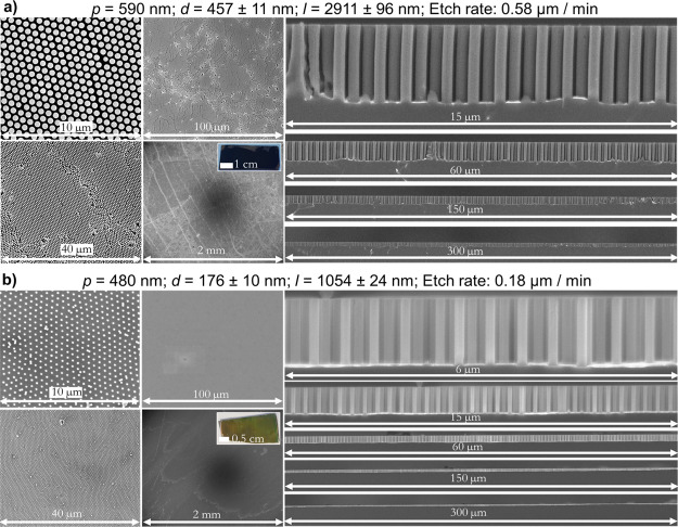
After properly designing the MACE experimental conditions, several batches of homogeneous Si wire arrays with a wide range of diameters (ca. 120–1050 nm) and pitches (480–1500 nm) could be reproducibly synthesized with a high throughput. Typical defects, such as grain boundaries and holes, are still visible on large-scale substrates, which can occasionally lead to local fractures of the gold film. However, the density of such defects was kept low using high-quality colloidal templates grown via self-assembly at the air–water interface (Figures 8, S7).50 Additionally, we validated our conclusions using an exceptionally homogeneous colloidal template based on the assembly of core–shell SiO2-PNiPAm spheres with an LB trough.8,38,51 Plasma etching of the polymeric shell yields a non-close-packed array of SiO2 particles which can then be used for colloidal lithography. The high monodispersity of the SiO2 core and the soft nature of the microgel shell that can locally compress to suppress defects provide a colloidal template of higher quality than those obtained with simple PS colloidal particles after plasma-induced size reduction. The resulting SiNW array was almost defect-free with an exceptionally flat gold film (Figure 8b), which we attribute to the highly homogeneous gold nanomeshes produced using these SiO2-PNiPAm spheres.
Figure 8.
Large-scale homogeneous Si nanowire arrays fabricated with MACE and colloidal lithography. Secondary electron top view or cross-sectional SEM images at different magnifications. The inset shows a photograph of the substrate. (a) AZO: 75 W 1 s; Au: 200 s 40 mA; HF/H2O2/H2O: 10:0.75:10 for 5 min. Prepared with PS colloidal particles. Images of large-scale homogeneous Si wire arrays of 1100 and 1500 nm pitches can be found in Figure S7. (b) AZO: 75 W 1 s; Au: 200 s 40 mA; HF/H2O2/H2O: 10:0.75:10 for 6 min. Prepared with SiO2-PNiPAm core–shell particles.
Based on the extensive analysis of our MACE experiments, we conclude that the following parameters are critical for proper MACE:
-
(i)
An adhesion layer is necessary to increase the Au–Si interaction and avoid film delamination during MACE.
-
(ii)
The Au film thickness needs to be sufficiently high to afford mechanical stability (i.e., >ca. 20 nm).
-
(iii)
A slow etch rate is necessary to avoid bending, fracture, and delamination of the gold film.
-
(iv)
The etch rate depends on the Au surface coverage, as well as the Au/Si/solution interface length (i.e., on both wire diameter and array pitch), and therefore needs to be optimized for each desired geometry.
-
(v)
The density of defects in the array (i.e., vacancies and grain boundaries) has a dramatic effect on gold film stability by locally changing the etch rate, which can lead to significant damages to the gold film and the substrate. The use of crystalline 2D templates with large grains can mitigate these issues. It is thus recommended to use high-quality colloidal monolayer templates8,38,51 or defect-free patterning techniques such as deep UV photolithography or e-beam lithography.
Conclusions
To conclude, we discuss the critical factors that influence the large-scale homogeneous etching of silicon micro- and nanowire arrays via the combined use of colloidal lithography and MACE. In particular, the influence of both Au coverage and Au/Si/etchant interface length on the etch rate is discussed for the first time. Our results demonstrate that the metal film fracture originates from adhesion problems, inappropriate film thickness, large etch rates, and local differences in the etch rate caused by small variations in the array geometry, directly related to the quality of the colloidal templates. Thus, MACE can be reliably performed over large areas only when using high-quality patterns, a sufficiently thick metal film, a proper adhesion layer, and relatively low etch rates. This work strengthens our understanding of MACE and outlines important guidelines to perform MACE across a wide range of array dimensions. Although our study focused on metal meshes prepared via colloidal lithography for the synthesis of VA-SiNW arrays, our findings apply to other patterning approaches, etching mask geometries, and potentially other semiconductors that can be structured via MACE.53,54 As such, our work should be of interest for new but also experienced researchers working with MACE.
Acknowledgments
We thank Grant Osborne for his help with the 3D-printer to prepare the sample holders used for MACE.
Glossary
Abbreviations
- d
diameter
- p
pitch
- l
length
- AZO
aluminum-doped zinc oxide
- MACE
metal-assisted chemical etching
- PS
polystyrene
- SEM
scanning electron microscopy
- SiNW
Si nanowire
- SLS
solution–liquid–solid
- VLS
vapor–liquid–solid
- VA-SiNW
vertically oriented Si nanowire
Supporting Information Available
The Supporting Information is available free of charge at https://pubs.acs.org/doi/10.1021/acs.chemmater.0c03593.
Materials, details of the experimental methods, and additional SEM images (PDF)
Author Contributions
The manuscript was written through contributions of all authors. All authors have given approval to the final version of the manuscript.
G.R.B. and F.J.W. gratefully acknowledge support from the Austrian Science Fund FWF for project P-33159. M.R. and N.V. acknowledge support by the Deutsche Forschungsgemeinschaft (DFG, German Research Foundation) Project-ID 416229255—SFB 1411 under grant number VO1824/6-1. N.V. also acknowledges support by the Interdisciplinary Center for Functional Particle Systems (FPS).
The authors declare no competing financial interest.
Supplementary Material
References
- Blick R. H.; Erbe A.; Pescini L.; Kraus A.; Scheible D. V.; Beil F. W.; Hoehberger E.; Hoerner A.; Kirschbaum J.; Lorenz H.; Kotthaus J. P. Nanostructured silicon for studying fundamental aspects of nanomechanics. J. Phys.: Condens. Matter 2002, 14, R905–R945. 10.1088/0953-8984/14/34/202. [DOI] [Google Scholar]
- Jiang Y.; et al. Rational Design of Silicon Structures for Optically Controlled Multiscale Biointerfaces. Nat. Biomed. Eng. 2018, 2, 508–521. 10.1038/s41551-018-0230-1. [DOI] [PMC free article] [PubMed] [Google Scholar]
- Priolo F.; Gregorkiewicz T.; Galli M.; Krauss T. F. Silicon nanostructures for photonics and photovoltaics. Nat. Nanotechnol. 2014, 9, 19–32. 10.1038/nnano.2013.271. [DOI] [PubMed] [Google Scholar]
- Sun L.; Xie J.; Jin Z. Different Dimensional Nanostructured Silicon Materials: From Synthesis Methodology to Application in High-Energy Lithium-Ion Batteries. Energy Technol. 2019, 7, 1900962. 10.1002/ente.201900962. [DOI] [Google Scholar]
- Wendisch F. J.; Abazari M.; Mahdavi H.; Rey M.; Vogel N.; Musso M.; Diwald O.; Bourret G. R. Morphology-Graded Silicon Nanowire Arrays via Chemical Etching: Engineering Optical Properties at the Nanoscale and Macroscale. ACS Appl. Mater. Interfaces 2020, 12, 13140–13147. 10.1021/acsami.9b21466. [DOI] [PMC free article] [PubMed] [Google Scholar]
- Seo K.; Wober M.; Steinvurzel P.; Schonbrun E.; Dan Y.; Ellenbogen T.; Crozier K. B. Multicolored Vertical Silicon Nanowires. Nano Lett. 2011, 11, 1851–1856. 10.1021/nl200201b. [DOI] [PubMed] [Google Scholar]
- Proust J.; Bedu F.; Gallas B.; Ozerov I.; Bonod N. All-Dielectric Colored Metasurfaces with Silicon Mie Resonators. ACS Nano 2016, 10, 7761–7767. 10.1021/acsnano.6b03207. [DOI] [PubMed] [Google Scholar]
- Rey B. M.; Elnathan R.; Ditcovski R.; Geisel K.; Zanini M.; Fernandez-Rodriguez M.-A.; Naik V. V.; Frutiger A.; Richtering W.; Ellenbogen T.; Voelcker N. H.; Isa L. Fully Tunable Silicon Nanowire Arrays Fabricated by Soft Nanoparticle Templating. Nano Lett. 2016, 16, 157–163. 10.1021/acs.nanolett.5b03414. [DOI] [PubMed] [Google Scholar]
- Cambiasso J.; König M.; Cortés E.; Schlücker S.; Maier S. A. Surface-Enhanced Spectroscopies of a Molecular Monolayer in an All-Dielectric Nanoantenna. ACS Photonics 2018, 5, 1546–1557. 10.1021/acsphotonics.7b01604. [DOI] [Google Scholar]
- Garnett E.; Yang P. Light Trapping in Silicon Nanowire Solar Cells. Nano Lett. 2010, 10, 1082–1087. 10.1021/nl100161z. [DOI] [PubMed] [Google Scholar]
- Kelzenberg M. D.; Boettcher S. W.; Petykiewicz J. A.; Turner-Evans D. B.; Putnam M. C.; Warren E. L.; Spurgeon J. M.; Briggs R. M.; Lewis N. S.; Atwater H. A. Enhanced Absorption and Carrier Collection in Si Wire Arrays for Photovoltaic Applications. Nat. Mater. 2010, 9, 239–244. 10.1038/NMAT2635. [DOI] [PubMed] [Google Scholar]
- Oh J.; Yuan H.-C.; Branz H. M. An 18.2%-Efficient Black-Silicon Solar Cell Achieved Through Control of Carrier Recombination in Nanostructures. Nat. Nanotechnol. 2012, 7, 743–748. 10.1038/NNANO.2012.166. [DOI] [PubMed] [Google Scholar]
- Savin H.; Repo P.; von Gastrow G.; Ortega P.; Calle E.; Garín M.; Alcubilla R. Black Silicon Solar Cells with Interdigitated Back-Contacts Achieve 22.1% Efficiency. Nat. Nanotechnol. 2015, 10, 624–628. 10.1038/NNANO.2015.89. [DOI] [PubMed] [Google Scholar]
- Deng J.; Su Y.; Liu D.; Yang P.; Liu B.; Liu C. Nanowire Photoelectrochemistry. Chem. Rev. 2019, 119, 9221–9259. 10.1021/acs.chemrev.9b00232. [DOI] [PubMed] [Google Scholar]
- Vijselaar W.; Westerik P.; Veerbeek J.; Tiggelaar R. M.; Berenschot E.; Tas N. R.; Gardeniers H.; Huskens J. Spatial Decoupling of Light Absorption and Catalytic Activity of Ni–Mo-Loaded High-Aspect-Ratio Silicon Microwire Photocathodes. Nat. Energy 2018, 3, 185–192. 10.1038/s41560-017-0068-x. [DOI] [Google Scholar]
- Su Y.; Liu C.; Brittman S.; Tang J.; Fu A.; Kornienko N.; Kong Q.; Yang P. Single-Nanowire Photoelectrochemistry. Nat. Nanotechnol. 2016, 11, 609–612. 10.1038/nnano.2016.30. [DOI] [PubMed] [Google Scholar]
- Alhmoud H. Z.; Guinan T. M.; Elnathan R.; Kobus H.; Voelcker N. H. Surface-assisted laser desorption/ionization mass spectrometry using ordered silicon nanopillar arrays. Analyst 2014, 139, 5999–6009. 10.1039/C4AN01391C. [DOI] [PubMed] [Google Scholar]
- Wagner R. S.; Ellis W. C. Vapor-Liquid-Solid Mechanism of Single Crystal Growth. J. Appl. Phys. 1964, 4, 89–90. 10.1063/1.1753975. [DOI] [Google Scholar]
- Morales A. M.; Lieber C. M. A Laser Ablation Method for the Synthesis of Crystalline Semiconductor Nanowires. Science 1998, 279, 208–211. 10.1126/science.279.5348.208. [DOI] [PubMed] [Google Scholar]
- Schmidt V.; Wittemann J. V.; Senz S.; Gösele U. Silicon Nanowires: A Review on Aspects of their Growth and their Electrical Properties. Adv. Mater. 2009, 21, 2681–2702. 10.1002/adma.200803754. [DOI] [PubMed] [Google Scholar]
- Chen W.; Yu L.; Misra S.; Fan Z.; Pareige P.; Patriarche G.; Bouchoule S.; Cabarrocas P. R. i. Incorporation and Redistribution of Impurities into Silicon Nanowires during Metal-Particle-Assisted Growth. Nat. Commun. 2014, 5, 4134. 10.1038/ncomms5134. [DOI] [PubMed] [Google Scholar]
- Wang F.; Dong A.; Buhro W. E. Solution-Liquid-Solid Synthesis, Properties, and Applications of One-Dimensional Colloidal Semiconductor Nanorods and Nanowires. Chem. Rev. 2016, 116, 10888–10933. 10.1021/acs.chemrev.5b00701. [DOI] [PubMed] [Google Scholar]
- Heitsch A. T.; Fanfair D. D.; Tuan H.-Y.; Korgel B. A. Solution-Liquid-Solid (SLS) Growth of Silicon Nanowires. J. Am. Chem. Soc. 2008, 130, 5436–5437. 10.1021/ja8011353. [DOI] [PubMed] [Google Scholar]
- Fu Y. Q.; Colli A.; Fasoli A.; Luo J. K.; Flewitt A. J.; Ferrari A. C.; Milne W. I. Deep Reactive Ion Etching as a Tool for Nanostructure Fabrication. J. Vac. Sci. Technol., B: Microelectron. Nanometer Struct.--Process., Meas., Phenom. 2009, 27, 1520. 10.1116/1.3065991. [DOI] [Google Scholar]
- Zhang X.; Lin J. K.; Wickramanayaka S.; Zhang S.; Weerasekera R.; Dutta R.; Chang K. F.; Chui K.-J.; Li H. Y.; Wee Ho D. S.; Ding L.; Katti G.; Bhattacharya S.; Kwong D.-L. Heterogeneous 2.5D integration on through silicon interposer. Appl. Phys. Rev. 2015, 2, 021308. 10.1063/1.4921463. [DOI] [Google Scholar]
- Huang Z.; Geyer N.; Werner P.; de Boor J.; Gösele U. Metal-Assisted Chemical Etching of Silicon: A Review. Adv. Mater. 2011, 23, 285–308. 10.1002/adma.201001784. [DOI] [PubMed] [Google Scholar]
- Huang Z.; Fang H.; Zhu J. Fabrication of Silicon Nanowire Arrays with Controlled Diameter, Length, and Density. Adv. Mater. 2007, 19, 744–748. 10.1002/adma.200600892. [DOI] [Google Scholar]
- Lai R. A.; Hymel T. M.; Narasimhan V. K.; Cui Y. Schottky Barrier Catalysis Mechanism in Metal-Assisted Chemical Etching of Silicon. ACS Appl. Mater. Interfaces 2016, 8, 8875–8879. 10.1021/acsami.6b01020. [DOI] [PubMed] [Google Scholar]
- Huang Z.; Shimizu T.; Senz S.; Zhang Z.; Zhang X.; Lee W.; Geyer N.; Gösele U. Ordered arrays of vertically aligned 110 silicon nanowires by suppressing the crystallographically preferred <100 etching directions. Nano Lett. 2009, 9, 2519–2525. 10.1021/nl803558n. [DOI] [PubMed] [Google Scholar]
- Choi W. K.; Liew T. H.; Dawood M. K.; Smith H. I.; Thompson C. V.; Hong M. H. Synthesis of silicon nanowires and nanofin arrays using interference lithography and catalytic etching. Nano Lett. 2008, 8, 3799–3802. 10.1021/nl802129f. [DOI] [PubMed] [Google Scholar]
- Lai C. Q.; Cheng H.; Choi W. K.; Thompson C. V. Mechanics of Catalyst Motion during Metal Assisted Chemical Etching of Silicon. J. Phys. Chem. C 2013, 117, 20802–20809. 10.1021/jp407561k. [DOI] [Google Scholar]
- Kong L.; Zhao Y.; Dasgupta B.; Ren Y.; Hippalgaonkar K.; Li X.; Chim W. K.; Chiam S. Y. Minimizing Isolate Catalyst Motion in Metal-Assisted Chemical Etching for Deep Trenching of Silicon Nanohole Array. ACS Appl. Mater. Interfaces 2017, 9, 20981–20990. 10.1021/acsami.7b04565. [DOI] [PubMed] [Google Scholar]
- Yeom J.; Ratchford D.; Field C. R.; Brintlinger T. H.; Pehrsson P. E. Decoupling Diameter and Pitch in Silicon Nanowire Arrays Made by Metal-Assisted Chemical Etching. Adv. Funct. Mater. 2014, 24, 106–116. 10.1002/adfm.201301094. [DOI] [Google Scholar]
- Wendisch F. J.; Oberreiter R.; Salihovic M.; Elsaesser M. S.; Bourret G. R. Confined Etching within 2D and 3D Colloidal Crystals for Tunable Nanostructured Templates: Local Environment Matters. ACS Appl. Mater. Interfaces 2017, 9, 3931–3939. 10.1021/acsami.6b14226. [DOI] [PubMed] [Google Scholar]
- Um H.-D.; Kim N.; Lee K.; Hwang I.; Hoon Seo J.; Yu Y. J.; Duane P.; Wober M.; Seo K. Versatile Control of Metal-Assisted Chemical Etching for Vertical Silicon Microwire Arrays and Their Photovoltaic Applications. Sci. Rep. 2015, 5, 11277. 10.1038/srep11277. [DOI] [PMC free article] [PubMed] [Google Scholar]
- Li L.; Liu Y.; Zhao X.; Lin Z.; Wong C.-P. Uniform vertical trench etching on silicon with high aspect ratio by metal-assisted chemical etching using nanoporous catalysts. ACS Appl. Mater. Interfaces 2014, 6, 575–584. 10.1021/am4046519. [DOI] [PubMed] [Google Scholar]
- Geyer N.; Fuhrmann B.; Huang Z.; de Boor J.; Leipner H. S.; Werner P. Model for the Mass Transport during Metal-Assisted Chemical Etching with Contiguous Metal Films As Catalysts. J. Phys. Chem. C 2012, 116, 13446–13451. 10.1021/jp3034227. [DOI] [Google Scholar]
- Tang J. S. J.; Bader R. S.; Goerlitzer E. S. A.; Wendisch J. F.; Bourret G. R.; Rey M.; Vogel N. Surface Patterning with SiO2@PNiPAm Core-Shell Particles. ACS Omega 2018, 3, 12089–12098. 10.1021/acsomega.8b01985. [DOI] [PMC free article] [PubMed] [Google Scholar]
- Kim J. D.; Mohseni P. K.; Balasundaram K.; Ranganathan S.; Pachamuthu J.; Coleman J. J.; Li X. Scaling the Aspect Ratio of Nanoscale Closely Packed Silicon Vias by MacEtch: Kinetics of Carrier Generation and Mass Transport. Adv. Funct. Mater. 2017, 27, 1605614. 10.1002/adfm.201605614. [DOI] [Google Scholar]
- Akan R.; Parfeniukas K.; Vogt C.; Toprak M. S.; Vogt U. Reaction Control of Metal-Assisted Chemical Etching for Silicon-Based Zone Plate Nanostructures. RSC Adv. 2018, 8, 12628–12634. 10.1039/c8ra01627e. [DOI] [PMC free article] [PubMed] [Google Scholar]
- Peng K. Q.; Hu J. J.; Yan Y. J.; Wu Y.; Fang H.; Xu Y.; Lee S. T.; Zhu J. Fabrication of Single-Crystalline Silicon Nanowires by Scratching a Silicon Surface with Catalytic Metal Particles. Adv. Funct. Mater. 2006, 16, 387–394. 10.1002/adfm.200500392. [DOI] [Google Scholar]
- Vogel N.; Goerres S.; Landfester K.; Weiss C. K. A Convenient Method to Produce Close- and Non-close-Packed Monolayers using Direct Assembly at the Air-Water Interface and Subsequent Plasma-Induced Size Reduction. Macromol. Chem. Phys. 2011, 212, 1719–1734. 10.1002/macp.201100187. [DOI] [Google Scholar]
- Lee S. H.; Bantz K. C.; Lindquist N. C.; Oh S.-H.; Haynes C. L. Self-Assembled Plasmonic Nanohole Arrays. Langmuir 2009, 25, 13685–13693. 10.1021/la9020614. [DOI] [PubMed] [Google Scholar]
- Vogel N.; Weiss C. K.; Landfester K. From Soft to Hard: The Generation of Functional and Complex Colloidal Monolayers for Nanolithography. Soft Matter 2012, 8, 4044–4061. 10.1039/C1SM06650A. [DOI] [Google Scholar]
- Lotito V.; Zambelli T. Pattern Detection in Colloidal Assembly: A Mosaic of Analysis Techniques. Adv. Colloid Interface Sci. 2020, 284, 102252. 10.1016/j.cis.2020.102252. [DOI] [PubMed] [Google Scholar]
- Rey M.; Law A. D.; Buzza D. M. A.; Vogel N. Anisotropic Self-Assembly from Isotropic Colloidal Building Blocks. J. Am. Chem. Soc. 2017, 139, 17464–17473. 10.1021/jacs.7b08503. [DOI] [PubMed] [Google Scholar]
- Rey M.; Yu T.; Bley K.; Landfester K.; Buzza D. M. A.; Vogel N. Amphiphile-Induced Anisotropic Colloidal Self-Assembly. Langmuir 2018, 34, 9990–10000. 10.1021/acs.langmuir.8b01382. [DOI] [PubMed] [Google Scholar]
- Fernández-Rodríguez M. Á.; Elnathan R.; Ditcovski R.; Grillo F.; Conley G. M.; Timpu F.; Rauh A.; Geisel K.; Ellenbogen T.; Grange R.; Scheffold F.; Karg M.; Richtering W.; Voelcker N. H.; Isa L. Tunable 2D Binary Colloidal Alloys for Soft Nanotemplating. Nanoscale 2018, 10, 22189–22195. 10.1039/C8NR07059H. [DOI] [PubMed] [Google Scholar]
- Wendisch F. J.; Saller M. S.; Eadie A.; Reyer A.; Musso M.; Rey M.; Vogel N.; Diwald O.; Bourret G. R. Three-Dimensional Electrochemical Axial Lithography on Si Micro- and Nanowire Arrays. Nano Lett. 2018, 18, 7343–7349. 10.1021/acs.nanolett.8b03608. [DOI] [PMC free article] [PubMed] [Google Scholar]
- Rey M.; Yu T.; Guenther R.; Bley K.; Vogel N. A Dirty Story: Improving Colloidal Monolayer Formation by Understanding the Effect of Impurities at the Air/Water Interface. Langmuir 2019, 35, 95–103. 10.1021/acs.langmuir.8b02605. [DOI] [PubMed] [Google Scholar]
- Rey M.; Fernandez-Rodriguez M. A.; Karg M.; Isa L.; Vogel N. Poly-N-isopropylacrylamide Nanogels and Microgels at Fluid Interfaces. Acc. Chem. Res. 2020, 53, 414–424. 10.1021/acs.accounts.9b00528. [DOI] [PubMed] [Google Scholar]
- Dawood M. K.; Liew T. H.; Lianto P.; Hong M. H.; Tripathy S.; Thong J. T. L.; Choi W. K. Interference Lithographically Defined and Catalytically Etched, Large-Area Silicon Nanocones from Nanowires. Nanotechnology 2010, 21, 205305. 10.1088/0957-4484/21/20/205305. [DOI] [PubMed] [Google Scholar]
- DeJarld M.; Shin J. C.; Chern W.; Chanda D.; Balasundaram K.; Rogers J. A.; Li X. Formation of High Aspect Ratio GaAs Nanostructures with Metal-Assisted Chemical Etching. Nano Lett. 2011, 11, 5259–5263. 10.1021/nl202708d. [DOI] [PubMed] [Google Scholar]
- Kim S. H.; Mohseni P. K.; Song Y.; Ishihara T.; Li X. Inverse Metal-Assisted Chemical Etching Produces Smooth High Aspect Ratio InP Nanostructures. Nano Lett. 2015, 15, 641–648. 10.1021/nl504136c. [DOI] [PubMed] [Google Scholar]
Associated Data
This section collects any data citations, data availability statements, or supplementary materials included in this article.


