Highlights
A self-powered α-In2Se3/3R MoS2 heterojunction is successfully developed and shows strong photo response to the visible and near infrared light.
The heterojunction photodetector delivers an ultrahigh photoresponsivity of 2.9 × 10³ A W−1 and a substantial specific detectivity of 6.2 × 10¹⁰ Jones under a compressive strain of − 0.26%.
This work demonstrates that the transport of photo generated carriers is clearly modulated by mechanical stimuli through the piezo-phototronic effect at the heterojunction interface.
Supplementary material
The online version contains supplementary material available at (10.1007/s40820-020-00584-1) contains supplementary material, which is available to authorized users.
Keywords: α-In2Se3/3R MoS2 heterojunction, Flexible, Self-powered photodetector, Strain modulation, Piezoelectric charge
Abstract
Semiconducting piezoelectric α-In2Se3 and 3R MoS2 have attracted tremendous attention due to their unique electronic properties. Artificial van der Waals (vdWs) heterostructures constructed with α-In2Se3 and 3R MoS2 flakes have shown promising applications in optoelectronics and photocatalysis. Here, we present the first flexible α-In2Se3/3R MoS2 vdWs p-n heterojunction devices for photodetection from the visible to near infrared region. These heterojunction devices exhibit an ultrahigh photoresponsivity of 2.9 × 10³ A W−1 and a substantial specific detectivity of 6.2 × 10¹⁰ Jones under a compressive strain of − 0.26%. The photocurrent can be increased by 64% under a tensile strain of + 0.35%, due to the heterojunction energy band modulation by piezoelectric polarization charges at the heterojunction interface. This work demonstrates a feasible approach to enhancement of α-In2Se3/3R MoS2 photoelectric response through an appropriate mechanical stimulus.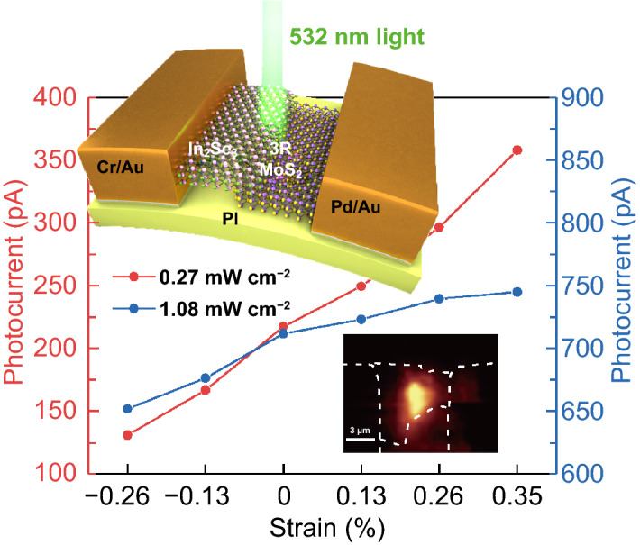
Supplementary material
The online version contains supplementary material available at (10.1007/s40820-020-00584-1) contains supplementary material, which is available to authorized users.
Introduction
Since discovery of graphene, various two-dimensional (2D) materials, like hexagonal boron nitride, transition-metal dichalcogenides, oxides and chalcogenides, etc. have been successfully assembled into van der Waals (vdWs) heterostructures, uncovering their unique physical properties and developing novel electronic, optoelectronic, ferroelectric, thermoelectric and electrochemistry devices [1–4]. In addition, these 2D materials are of excellent mechanical properties which endow them a huge advantage in flexible electronic applications over conventional crystalline semiconductors which are very brittle. With appropriate stackings of these two-dimensional vdW materials, p–n junctions can form for the sake of development of flexible electronic and optoelectronic devices. Among these 2D materials, several ultrathin layers with non-centrosymmetric structure are of piezoelectricity and they are the most promising for mechanically modulated electronic and optoelectronic applications through mechanical agitations, like wurtzite structure material ZnO [5, 6]. Monolayer MoS2 has been employed to develop optoelectronic devices in which strain-induced piezoelectric polarization charges are utilized to modulate photoexcited carrier transport and recombination at the Schottky barrier or p–n junction interfaces. This strain-modulated process is called the piezo-phototronic effect [7–10]. However, the piezoelectricity of 2H MoS2 is restricted in odd few layers and it is significantly weakened with increasing the thickness [11]. In contrast, due to broken inversion symmetry, 3R MoS2 exhibits piezoelectricity from monolayer to the bulk, having an exciting potential for nonlinear optics, valley-dependent spin polarization, and advancing flexible wearable electronics [12, 13]. In addition, indium selenide, a direct bandgap and layered structure III–V compound, has recently attracted enormous attention, due to its superior electric, piezoelectric, thermoelectric, photoelectric and electrochemical properties [14–19]. Ding et al. theoretically revealed that In2Se3 and other III2-V3 van der Waals materials exhibit room-temperature ferroelectricity, originated from both spontaneous in-plane and out-of-plane electric polarization [20]. It is widely accepted that all ferroelectric materials are also piezoelectric [21, 22]. Indeed, the in-plane and out-plane ferroelectric and piezoelectric properties have been confirmed and characterized experimentally in α and β phase In2Se3 [23–26]. Theoretically speaking, controllable energy band alignment in a 3R MoS2 and In2Se3 heterostructure could be realized through an applied electric field, to achieve a broad spectrum of light absorption for novel tunable optoelectronic applications [27].
In this paper, we report on the first self-powered n-type α-In2Se3/p-type 3R MoS2 heterojunction photodetectors built on flexible substrate. These photodetectors show a good current rectification characteristic, ultrahigh photocurrent generation efficiency and highly sensitive photoresponse from the visible to near infrared region. The transport of photocarriers is strain-modulated at the heterojunction interface through the piezo-phototronic effect. With a + 0.35% tensile strain, the photocurrent can be enhanced by 64%, mainly promoted by piezoelectric polarization from In2Se3, and type-II band alignment between α-In2Se3 and 3R MoS2, which enhances the built-in electric field in the p-n heterojunction, in favor of photocarriers separation. To achieve high mechanical durability [28] and light absorption, the heterojunctions to be presented here were constructed with multilayer α-In2Se3 and 3R MoS2 flakes.
Experimental Section
Synthesis of α-In2Se3/3R MoS2 Heterojunction and the Device Fabrication
The device substrate was fabricated by spinning coating polyimide on a flexible polished stainless steel at 3000 rpm for 45 s, and then, annealed in argon gas at 250 °C for 2 h. The 3R MoS2 flakes were mechanically exfoliated from a chemical vapor deposition (CVD) synthesized bulk 3R MoS2 crystal onto the polyimide thin film. The surfaces of the MoS2 flakes were then treated with CHF3 plasma doping in a PlasmaThermo 790 MF Reactive ion etch (RIE) system. For the plasma doping, the RF power, gas pressure, precursor gas flow and process time were 100 W, 10 mTorr, 10 sccm, and 45 s, respectively. The bulk α-In2Se3 was bought on market and mechanically exfoliated onto the plasma treated 3R MoS2 flakes/polyimide. The overlapped α-In2Se3/3R MoS2 flakes were identified using optical microscopy. Cr/Au (10/150 nm) was deposited on the α-In2Se3 flakes and Pd/Au (10/150 nm) was coated on the 3R MoS2 flakes, using an e-beam evaporator and then patterned through a lift-off process.
Materials Characterization
The atomic force microscopy (AFM) characterization (Cypher S Asylum Research Oxford Instruments) was carried out using non-contact mode. XPS measurements were conducted on a Kratos AXIS Supra X-ray photoelectron spectrometer.
The SHG measurement utilized a mode-locked Ti:sapphire laser (output wavelength: 800 nm and repetition rate: 76 MHz) to generate tunable wavelength light ranging from 500 to 1600 nm filtered through OPO, then circularly polarized by the quarter-wave plate, attenuated and focused on a sample by microscope objective lens (100 × , NA = 0.95). The SHG signal was collected by the same lens using a dichroic mirror and filtered by a short pass filter before entering a spectrometer.
The Raman scattering measurements (WITec alpha 300 confocal Raman microscopy) were carried out under a laser light of 532 nm, laser power of 0.1 mW and beam diameter of 400 nm with a 100 × objective lens.
Electrical, Optoelectronic, and Mechanical Characterizations
The electrical characteristic measurements were performed using a Keysight B1500A Semiconductor Device Parameter Analyzer. 532 and 800 nm wavelength light with tunable intensity were obtained from a Quartz Halogen light system and a monochromator for the photovoltaic and photo-sensing measurement. The strains were applied through a home-made two-point bending apparatus. The strains applied were calculated through the bending angles (referring to the supporting document). For the spatial photocurrent mapping, the sample was fixed on the motorized stage in WITec alpha 300 confocal Raman microscopy with a continuous 532 nm laser with a beam diameter of 400 nm. The photocurrent was measured using Keithley 2450 sourcemeter, and a Femto DLPCA-200 universal low noise current amplifier.
Results and Discussion
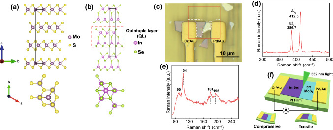
3R MoS2 is of a broken symmetry, regardless of the layer number, by repeating ABC-ABC stacking order, where A, B, C are three same monolayer MoS2 in the same direction with a shift, as shown in Fig. 1a for the side and top views. Therefore, 3R MoS2 is piezoelectric and its piezoelectric coefficient e11 is theoretically calculated to be around 0.40 C m−2 for 1–6 layers and 0.30 C m−2 for the bulk [13]. Our recent piezoelectric force microscopy (PFM) measurements suggest an out-of-plane piezoelectric coefficient d33 of 1.2 pm V−1 for a 28 nm thick 3R MoS2 flake [29]. α-In2Se3 typically has hexagonal or rhombohedral atomic structures. Both structures have primary quintuple layers in different stacking orders. A single quintuple layer consists of five alternately arranged Se–In–Se–In–Se atomic layers, as illustrated in Fig. 1b. Hexagonal α-In2Se3 at any thickness possesses non-centrosymmetric property along the vertical direction, leading to the out-of-plane piezoelectricity (d33). In a single quintuple layer, one In atom and two Se atoms are located at nonequivalent sites of the hexagonal structure, generating the in-plane (d11) piezoelectricity under a planar strain. Recent theoretical calculation suggests a higher magnitude d13 than that of d33, implying that a significant vertical piezoelectric polarization could be induced under an in-plane strain. Bilayer hexagonal α-In2Se3 constructed by two dislocated quintuple layers results in the reservation of non-centrosymmetry, so does a multilayer hexagonal α-In2Se3 flake. Thus, hexagonal α-In2Se3 is of in-plane and out-of-plane piezoelectricity at any thickness [20, 23, 24, 30].
Fig. 1.
Atomic structures of 3R phase MoS2 and Hexagonal α-In2Se3, and optical, Raman spectra, electrical measurement setup of an α-In2Se3/3R MoS2 heterojunction. a Side and top view of 3R MoS2 atomic structure. The purple and yellow spheres correspond to molybdenum and sulfur atoms, respectively. b Side and top view of hexagonal α-In2Se3 atomic structure. The pink and green spheres correspond to indium and selenide atoms, respectively. c Optical image of the heterojunction on a flexible substrate. d Raman spectrum of the 3R MoS2 flake. e Raman spectrum of the α-In2Se3 flake under the excitation of 532 nm wavelength laser. f Schematic diagram of the heterojunction on a flexible substrate
To prepare a heterojunction of 3R MoS2 & α-In2Se3 flakes, the flakes were mechanically exfoliated from 3R MoS2 and α-In2Se3 crystals and then deposited on a clean flexible polyimide thin film in sequence. As shown in Fig. 1c, a location with a 3R MoS2 flake overlapped with an α-In2Se3 flake was selected through an optical microscope. Two characteristic Raman peaks shown in Fig. 1d, in-plane mode () and out-of-plane mode (), were observed from the bottom 3R MoS2 flake and the polarization-resolved second-harmonic generation (SHG) measurement evidenced a non-centrosymmetric structure from sixfold pattern (see Fig. S1), confirming that the bottom flake was indeed a 3R MoS2 flake. Four characteristic Raman peaks at 90, 104, 180, and 195 cm−1 from the top flake (shown in Fig. 1e) indicate a hexagonal structure of an α-In2Se3 flake. Furthermore, the bottom 3R MoS2 flake was p-type semiconducting after CHF3 plasma treatment and the top α-In2Se3 was n-type, as characterized by the x-ray photoelectron spectroscopy (XPS) measurement described in Fig. S1 [31–34]. A Cr/Au (10/150 nm) electrode and a Pd/Au (10/150 nm) electrode were deposited on the α-In2Se and 3R MoS2 flakes, respectively, to achieve ohmic contacts as explained in Fig. S2. The device and the circuit connection are illustrated in Fig. 1f. To study the strain modulation on the p–n heterojunction, the uniaxial compressive and tensile strains were applied through bending the flexible device downward and upward, see the insets in Fig. 1f. The strains applied were calculated with the bending angles as discussed in Fig. S3. The flexible heterojunction was characterized by a semiconductor parameter analyzer (Agilent B1500A) under different wavelength illumination and intensities from a Quartz Halogen light system through a monochromator. The morphology and height profiles of the heterojunction showed that the thickness of the 3R MoS2 and α-In2Se3 flakes was 30 and 206 nm, respectively (Fig. S4).
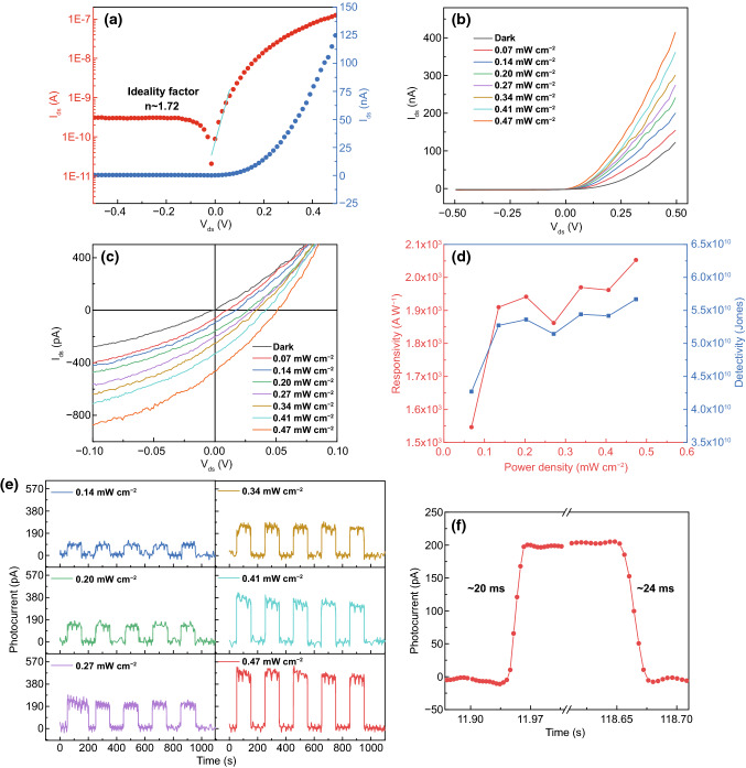
The dark I-V characteristic from the heterojunction device, as shown in Fig. 2a, was measured under the strain-free condition. The ideality factor was found to be 1.72 and the rectification factor under bias voltages of ± 0.5 V was 405. The observed excellent rectification characteristic indicates formation of a high-quality p–n junction. Under 532 nm light illumination with an intensity of 0.47 mW cm−2 and a bias voltage of + 0.5 V, a fourfold rise in the current, Ids, from 123 nA in the dark to 415 nA was observed, see Fig. 2b. The I–V characteristics measured under the intensity from 0.07 to 0.47 mW cm−2 and bias voltage of ± 0.1 V are shown in Fig. 2c. The photoresponsivity , (where Pt and A are the illumination intensity and effective area of the heterojunction), was found to be 2.1 × 10³ A W−1 at an intensity of 0.47 mW cm−2. Compared with those 2D materials-based photodetectors reported by other groups, especially the heterojunction devices listed in Table 1, our p–n heterojunction device has showed an ultrahigh photoresponsivity at a very low bias voltage, owing to a higher photocurrent generation efficiency and lower power consumption [35, 36]. The specific detectivity,, (where R and q are the responsivity and elementary charge), is usually used to tell the capability of detecting the incident photons. The D* value for our device was about 5.7 × 10¹⁰ Jones at the intensity of 0.47 mW cm−2, showing a good sensitivity to the light. The R and D* under several illumination intensities and a bias voltage of + 0.5 V are given in Fig. 2d. Under zero bias voltage and the light intensity of 0.27 mW cm−2, the R and D* were 2.5 A W−1 and 2.1 × 10¹⁰ Jones, respectively. Therefore, this α-In2Se3/3R MoS2 heterojunction could function as a self-powered photodetector. The photocurrent could stabilize from 100 to 500 pA under various light intensities with the rise and fall time of 20 and 24 ms shown in Fig. 2e, f. This device demonstrated a faster light response than most of the In2Se3 based photodetectors developed by other groups [18, 37–40]. Recent theoretical calculation predicts that the photocurrent generation from a α-In2Se3/3R MoS2 heterojunction could cover from visible light to near infrared region, with a higher optical absorption coefficient and current density than an isolated In2Se3 layer [27]. Indeed, infrared photoresponse from few layer β-In2Se3/monolayer MoS2 heterojunctions showed an extended detection range from the visible to near infrared region [37], due to the relatively small bandgap of β-In2Se3. As few layer β-In2Se3 and monolayer MoS2 were involved, the light absorption of their devices could not be high. The photoresponse from our α-In2Se3/3R MoS2 heterojunction devices did cover the visible and near infrared regions, as shown in Fig. S5. Compared with their results, our device showed superior performance with three orders higher responsivity and detectivity. It is easily found from Fig. S5c, e that the photocurrent under 532 nm illumination was around four times larger than that under 800 nm illumination, very likely due to weak light absorption in the near infrared region [41].
Fig. 2.
Electrical characterization and photoresponse from the α-In2Se3/3R MoS2 heterojunction under zero strain. a I–V characteristic in the dark with the logarithmic and linear scale. b, c I–V characteristics in the dark and under illumination of 532 nm wavelength under different light intensities from − 0.5 to 0.5 and − 0.1 to 0.1 V, respectively. d Responsivity and detectivity at a bias voltage of 0.5 V as a function of illumination intensities. e Current vs time under 532 nm illumination with several intensities and zero bias voltage. f Current vs time extracted from e under the illumination intensity of 0.27 mW cm−2
Table 1.
Comparison of the characteristic parameters of our present heterojunction devices with other 2D materials-based photo devices
| Materials | λ (nm) | Vbias (V) | Responsivity (A W−1) | Detectivity (D*) | Response time (ms) | Refs |
|---|---|---|---|---|---|---|
| α-In2Se3/3R MoS2 | 532 | 0.5 | 2052 | 5.7 × 10¹⁰ | 20 | This work |
| MoS2 Monolayer | 442 | 2 | 2.3 × 10⁴ | NA | NA | [7] |
| MoS2 Monolayer | 532 | − 10 | 1162 | 1.7 × 10¹² | NA | [8] |
| MoS2 Multilayer | 532 | 1.2 | 59 | NA | 0.042 | [35] |
| α-In2Se3 Monolayer | 532 | 2 | 340 | NA | 6 | [15] |
| α-In2Se3 Nanosheets | 300 | 5 | 395 | 2.3 × 10¹² | 18 | [16] |
| In2Se3 nanosheets | 532 | 5 | 20.5 | 6.0 × 10¹¹ | 24.6 | [17] |
| β-In2Se3 flake | 650 | 20 | 3.8 | 1 × 10¹⁰ | 3870 | [18] |
| WSe2/CdS | 680 | 2 | 33.4 | NA | NA | [36] |
| MoS2 /WSe2 | 532 | NA | 1.8 × 10⁻³ | NA | NA | [9] |
| β-In2Se3 /MoS2 | 450 | 1 | 4.47 | 1.1 × 10⁹ | 52 | [37] |
| MoS2 /GaN | 365/685 | 20 |
127 @ 365 33 @ 685 |
1.1 × 10¹¹ |
1500 @ 365 8000 @ 685 |
[38] |
| β-In2Se3 /GaN | 365/685 | 20 |
1.6 @ 365 0.3 @ 685 |
1.6 × 10⁹ |
210 @ 365 2300 @ 685 |
[38] |
| CuO/MoS2 | 432 | 10 | NA | 3.3 × 10⁸ | NA | [10] |
| WSe2/α-In2Se3 | 650 | − 1 | 0.026 | NA | 2.3 | [39] |
| GaN/α-In2Se3 | 365/850 | 3 |
127 @ 365 33 @ 850 |
3.6 × 10¹⁰ @ 850 |
130 @ 365 200 @ 850 |
[40] |
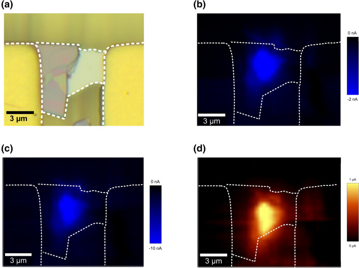
To tell that the photoresponse was dominated by the heterojunction, rather than from the α-In2Se3 or 3R MoS2 flake, a scanning photocurrent microscopic image (SPCM) was performed on the entire area between the two electrodes using a WITec Raman system with laser light of 532 nm at a power of 0.1 mW (See Experimental section for experimental setup). The SPCM images shown in Fig. 3 clearly displayed that it was only in the heterojunction area where the photocurrent was apparently generated when the α-In2Se3/3R MoS2 heterojunction was applied with a reverse bias of − 0.25 V, zero bias and a forward bias of 0.25 V.
Fig. 3.
Optical scanning photocurrent images of the α-In2Se3/3R MoS2 heterojunction. a The optical image. b–d Photocurrent mapping of the heterojunction under zero bias, reverse bias of − 0.25 V and forward bias of 0.25 V at 532 nm with a laser power of 0.1 mW and a spot waist radius of 400 nm
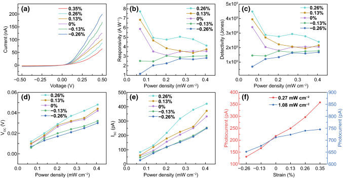
To study the influence of strains on photoresponse, the photocurrent was measured under different strains and light intensities. The I–V curves under various strains in dark are displayed in Fig. 4a. Apparent strain-modulated I–V characteristics can be seen with enhancing (weakening) rectification characteristics under compressive (tensile) strains. With a bias voltage of + 0.5 V, the current Ids was increased from 136 to 200 pA under a compressive strain of − 0.26% and decreased to 65 pA under a tensile strain of + 0.35%. Upon a compressive strain of − 0.26%, the responsivity increased from 1.5 × 10³ to 2.9 × 10³ A W−1, by 88%, while the detectivity rose from 4.3 × 10¹⁰ Jones to 6.2 × 10¹⁰ Jones, by 46% (Fig. S6e, f). Under a bias voltage of − 0.1 V, the strain modulations of the responsivity and detectivity occurred at a low illumination intensity of 0.07 mW cm−2 were much more significant than at a high intensity of 0.41 mW cm−2, as shown in Fig. 4b, c. The responsivity and detectivity decreased by 80% (from 5.9 to 1.2 A W−1) and 80% (3.4 × 10⁹ to 6.9 × 10⁸ Jones), under a compressive strain of − 0.26%. The open circuit voltage Voc and short circuit current Isc were increased with increasing the tensile strain but decreased with increasing the compressive strain as shown in Fig. 4d, e. In Fig. 4f, under a low light intensity of 0.27 mW cm−2, the photocurrent was increased from 220 to 360 pA (by 64%) up on a tensile strain of + 0.35%, but decreased from 220 to 130 pA (by 41%) with a compressive strain of − 0.26%. In contrast, under a high illumination intensity of 1.08 mW cm−2, it was only increased from 710 to 750 pA (by 5.6%) under the tensile strain and decreased from 710 to 650 pA (by 8.5%) under the compressive strain. The photocurrents as a function of time under 0.27 mW/cm2 and 1.08 mW cm−2 were also shown in Fig. S8. Illumination intensity dependent strain modulation of the photocurrent may not be accounted for by the strain-induced optical light absorption coefficient change in the 2D vdWs flakes, as the theoretical calculation has indicated that only a small change in light absorption coefficient in a 2% strained In2Se3/MoS2 heterojunction from ultraviolet to near-infrared light range [41]. As the strains applied in this study were much smaller than 2%, the strain-induced optical light absorption coefficient change in the 2D flakes can be ignored. In Fig. S2, the In2Se3 and MoS2 devices with good ohmic contacts did not show detectable electrical transport modulation under mechanical strains. These phenomena rule out the contribution from piezoresistive effect. Instead, the findings could be well interpreted using a piezoelectric potential originated from the piezoelectric charges at the heterojunction interface.
Fig. 4.
The strain-modulated photoresponse to 523 nm illumination from the α-In2Se3/3R MoS2 heterojunction. a I–V characteristic of the device under several strains in dark. b, c Responsivity and detectivity under − 0.1 V bias voltage. d, e Open circuit voltage Voc and short circuit current Isc under various light intensities and strains (The data were extracted from Fig. S7). f Average photocurrent as a function of strains under zero bias at the illumination intensities of 0.27 and 1.08 mW cm−2 (The data were extracted from Fig. S8)
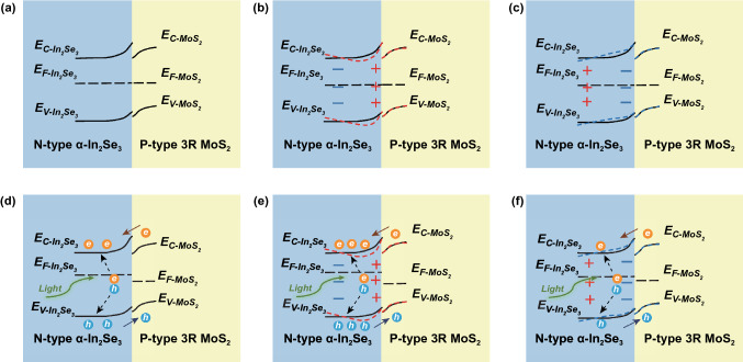
To interpret the strain-modulated photoresponse, the energy band diagrams of the heterojunction are plotted in Fig. 5. When a 3R MoS2 flake (with an indirect band gap of 1.29 eV and a higher electron affinity of 4.0 eV) is in contact with an α-In2Se3 flake (having a direct band gap of 1.55 eV and a lower electron affinity of 3.6 eV) [31, 41–45], a negative (positive) space charge region in the 3R MoS2 (α-In2Se3) flake is established, forming a p-n heterojunction in the thermal equilibrium under zero strain. The widths of the depletion region located in 3R MoS2 and α-In2Se3 sides can be estimated using the depletion model for a conventional p–n heterostructure, i.e. and , where and are the doping concentrations in the 3R MoS2 and α-In2Se3 flakes, respectively; is the built-in voltage; q is the elementary charge, and are the permittivity of 3R MoS2 and α-In2Se3 flakes, respectively [46–49]. As the carrier concentration, layer thickness and permittivity for the MoS2 (In2Se3) flake are cm−3, nm, () [50–53]. where is the permittivity in vacuum, the doping concentration could be estimated as cm−3. The built-in voltage V, for the type II band alignment, and the depletion width in the 3R MoS2 (α-In2Se3) flake should be () nm. As the depletion width in the MoS2 flake exceeded the thickness of MoS2 flake, the 3R MoS2 could be fully depleted. Since the theoretical d13 magnitude of α-In2Se3 is 3.08 pm V−1, a factor of 15 larger than that of 3R MoS2, we could ignore the out-of plane piezoelectric polarization in the 3R MoS2 flake for simplicity of discussion [30, 54]. Under a tensile (compressive) strain in dark, positive (negative) piezoelectric charges could emerge at the bottom surface of the α-In2Se3 flake [50]. The positive (negative) piezoelectric charges lower (raise) the energy band near the interface of the α-In2Se3 flake, as shown in Fig. 5b, c. The total internal electric field is enhanced (weakened) so that the potential barrier height is increased (decreased) in comparison with the condition of zero strain. As a result, the current under a forward bias would be reduced (enhanced) so that the rectification factor was found to be smaller (larger) under a tensile (compressive) strain, as shown in Fig. 4a. Upon illumination, only those electron–hole pairs created in or near the heterojunction could be separated by the built-in electric field with electrons (holes) being swept into α-In2Se3 (3R MoS2), giving rise to a photocurrent, see Fig. 5d. Upon a tensile (compressive) strain applied, the total internal electric field is enhanced (weakened) and the electric potential difference is then increased (decreased) in the heterojunction as discussed above, in favor of (weakening) separation of the electron–hole pairs and injection efficiency in or near the heterojunction (Fig. 5e, f), causing Voc and Isc increasing (decreasing) with raising tensile (compressive) strain, as shown in Fig. 4d, e. At a high illumination intensity, the number of electron hole pairs in or near the heterojunction is greatly increased so that the piezoelectric polarization charges could be effectively screened. This could equivalently reduce strain modulation effect [7–9], in consistence with our experimental finding of the light intensity dependence of the photocurrent modulation in Fig. 4.
Fig. 5.
The energy band diagrams for the α-In2Se3/3R MoS2 heterojunction with\without the strains and light illumination. The energy band diagram a in thermal equilibrium with zero light illumination and no external strain b under zero light illumination, a tensile strain c under zero light illumination, a compressive strain d under light illumination, no strain applied e under light illumination, a tensile strain f under light illumination and a compressive strain
Conclusion
High performance flexible heterojunction photodetectors have been successfully developed by stacking an α-In2Se3 flake with a 3R MoS2 flake. The devices showed clear photocurrent response to visible and near infrared light. The photocurrent response was found to be enhanced (reduced) with a tensile (compressive) strain and the strain modulation of the photocurrent response was much more significantly under weak illumination than under strong illumination. The strain modulation can be interpreted from the strain-induced piezoelectric polarization charges, which alter the total internal electric field in the heterojunction, promoting (weakening) collection of the photocarriers.
Electronic supplementary material
Below is the link to the electronic supplementary material.
Acknowledgements
This project is financially supported by MOE AcRF Tier2 (2018-T2-2-005), MOE AcRF Tier1 (2018-T1-005-001) and A*STAR AME IRG Grant SERC A1983c0027, Singapore.
References
- 1.Geim AK, Grigorieva IV. Van der waals heterostructures. Nature. 2013;499(7459):419–425. doi: 10.1038/nature12385. [DOI] [PubMed] [Google Scholar]
- 2.Xia W, Dai L, Yu P, Tong X, Song W, et al. Recent progress in van der waals heterojunctions. Nanoscale. 2017;9(13):4324–4365. doi: 10.1039/C7NR00844A. [DOI] [PubMed] [Google Scholar]
- 3.Wu J, Chen Y, Wu J, Hippalgaonkar K. Perspectives on thermoelectricity in layered and 2D materials. Adv. Electron. Mater. 2018;4(12):1800248. doi: 10.1002/aelm.201800248. [DOI] [Google Scholar]
- 4.Dryfe RAW. 2D transition metal chalcogenides and van der waals heterostructures: fundamental aspects of their electrochemistry. Curr. Opin. Electrochem. 2019;13:119–124. doi: 10.1016/j.coelec.2018.11.021. [DOI] [Google Scholar]
- 5.Wang ZL. Piezoelectric nanogenerators based on zinc oxide nanowire arrays. Science. 2006;312(5771):242–246. doi: 10.1126/science.1124005. [DOI] [PubMed] [Google Scholar]
- 6.Wu W, Wen X, Wang ZL. Taxel-addressable matrix of vertical-nanowire piezotronic transistors for active and adaptive tactile imaging. Science. 2013;340(6135):952–957. doi: 10.1126/science.1234855. [DOI] [PubMed] [Google Scholar]
- 7.Wu W, Wang L, Yu R, Liu Y, Wei S-H, et al. Piezophototronic effect in single-atomic-layer MoS2 for strain-gated flexible optoelectronics. Adv. Mater. 2016;28(38):8463–8468. doi: 10.1002/adma.201602854. [DOI] [PubMed] [Google Scholar]
- 8.Zhang K, Zhai J, Wang ZL. A monolayer MoS2 p-n homogenous photodiode with enhanced photoresponse by piezo-phototronic effect. 2D Mater. 2018;5(3):035038. doi: 10.1088/2053-1583/aac96b. [DOI] [Google Scholar]
- 9.Lin P, Zhu L, Li D, Xu L, Pan C, et al. Piezo-phototronic effect for enhanced flexible MoS2/WSe2 van der waals photodiodes. Adv. Funct. Mater. 2018;28(35):1802849. doi: 10.1002/adfm.201802849. [DOI] [Google Scholar]
- 10.Zhang K, Peng M, Wu W, Guo J, Gao G, et al. A flexible p-CuO/n-MoS2 heterojunction photodetector with enhanced photoresponse by the piezo-phototronic effect. Mater. Horiz. 2017;4(2):274–280. doi: 10.1039/C6MH00568C. [DOI] [Google Scholar]
- 11.Wu W, Wang L, Li Y, Zhang F, Lin L, et al. Piezoelectricity of single-atomic-layer MoS2 for energy conversion and piezotronics. Nature. 2014;514(7523):470–474. doi: 10.1038/nature13792. [DOI] [PubMed] [Google Scholar]
- 12.Shi J, Yu P, Liu F, He P, Wang R, et al. 3R MoS2 with broken inversion symmetry: a promising ultrathin nonlinear optical device. Adv. Mater. 2017;29(30):1701486. doi: 10.1002/adma.201701486. [DOI] [PubMed] [Google Scholar]
- 13.Tan D, Willatzen M, Wang ZL. Prediction of strong piezoelectricity in 3R-MoS2 multilayer structures. Nano Energy. 2019;56:512–515. doi: 10.1016/j.nanoen.2018.11.073. [DOI] [Google Scholar]
- 14.Han G, Chen Z-G, Drennan J, Zou J. Indium selenides: structural characteristics, synthesis and their thermoelectric performances. Small. 2014;10(14):2747–2765. doi: 10.1002/smll.201400104. [DOI] [PubMed] [Google Scholar]
- 15.Zhou J, Zeng Q, Lv D, Sun L, Niu L, et al. Controlled synthesis of high-quality monolayered α-In2Se3 via physical vapor deposition. Nano Lett. 2015;15(10):6400–6405. doi: 10.1021/acs.nanolett.5b01590. [DOI] [PubMed] [Google Scholar]
- 16.Jacobs-Gedrim RB, Shanmugam M, Jain N, Durcan CA, Murphy MT, et al. Extraordinary photoresponse in two-dimensional In2Se3 nanosheets. ACS Nano. 2014;8(1):514–521. doi: 10.1021/nn405037s. [DOI] [PubMed] [Google Scholar]
- 17.Zheng ZQ, Yao JD, Yang GW. Growth of centimeter-scale high-quality In2Se3 films for transparent, flexible and high performance photodetectors. J. Mater. Chem. C. 2016;4(34):8094–8103. doi: 10.1039/C6TC02296K. [DOI] [Google Scholar]
- 18.Mech RK, Solanke SV, Mohta N, Rangarajan M, Nath DN. In2Se3 visible/near-ir photodetector with observation of band-edge in spectral response. IEEE Photon. Technol. Lett. 2019;31(11):905–908. doi: 10.1109/LPT.2019.2912912. [DOI] [Google Scholar]
- 19.Jiang Y, Wang Q, Han L, Zhang X, Jiang L, et al. Construction of In2Se3/MoS2 heterojunction as photoanode toward efficient photoelectrochemical water splitting. Chem. Eng. J. 2019;358:752–758. doi: 10.1016/j.cej.2018.10.088. [DOI] [Google Scholar]
- 20.Ding W. Prediction of intrinsic two-dimensional ferroelectrics in In2Se3 and other In2Se3 van der waals materials. Nat. Commun. 2017;8(1):14956. doi: 10.1038/ncomms14956. [DOI] [PMC free article] [PubMed] [Google Scholar]
- 21.Bowen CR, Kim HA, Weaver PM, Dunn S. Piezoelectric and ferroelectric materials and structures for energy harvesting applications. Energy Environ. Sci. 2014;7(1):25–44. doi: 10.1039/C3EE42454E. [DOI] [Google Scholar]
- 22.Zhang Y, Jie W, Chen P, Liu W, Hao J. Ferroelectric and piezoelectric effects on the optical process in advanced materials and devices. Adv. Mater. 2018;30(34):1707007. doi: 10.1002/adma.201707007. [DOI] [PubMed] [Google Scholar]
- 23.Xue F, Zhang J, Hu W, Hsu W-T, Han A, et al. Multidirection piezoelectricity in mono- and multilayered hexagonal α-In2Se3. ACS Nano. 2018;12(5):4976–4983. doi: 10.1021/acsnano.8b02152. [DOI] [PubMed] [Google Scholar]
- 24.Zhou Y, Wu D, Zhu Y, Cho Y, He Q, et al. Out-of-plane piezoelectricity and ferroelectricity in layered α-In2Se3 nanoflakes. Nano Lett. 2017;17(9):5508–5513. doi: 10.1021/acs.nanolett.7b02198. [DOI] [PubMed] [Google Scholar]
- 25.Xue F, Hu W, Lee K-C, Lu L-S, Zhang J, et al. Room-temperature ferroelectricity in hexagonally layered α- In2Se3 nanoflakes down to the monolayer limit. Adv. Funct. Mater. 2018;28(50):1803738. doi: 10.1002/adfm.201803738. [DOI] [Google Scholar]
- 26.Zheng C, Yu L, Zhu L, Collins JL, Kim D, et al. Room temperature in-plane ferroelectricity in van der waals In2Se3. Sci. Adv. 2018;4(7):eaar7720. doi: 10.1126/sciadv.aar7720. [DOI] [PMC free article] [PubMed] [Google Scholar]
- 27.Zhou B. Enhanced carrier separation in ferroelectric In2Se3/MoS2 van der waals heterostructure. J. Mater. Chem. C. 2020;8:11160–11167. doi: 10.1039/d0tc02366c. [DOI] [Google Scholar]
- 28.Lee J-H, Park JY, Cho EB, Kim TY, Han SA, et al. Reliable piezoelectricity in bilayer WSe2 for piezoelectric nanogenerators. Adv. Mater. 2017;29(29):1606667. doi: 10.1002/adma.201606667. [DOI] [PubMed] [Google Scholar]
- 29.H. Hallil, W. Cai, K. Zhang, P. Yu, S. Liu, R. Xu, C. Zhu, Q. Xiong, Z. Liu, Q. Zhang, Observation of strong piezoelectricity in 3R-MoS2 flakes. In Progress.
- 30.Shuoguo Y. 2d ferroelectricity and piezoelectricity for electronic devices. Hung Hom: The Hong Kong Polytechnic University; 2020. [Google Scholar]
- 31.Poh SM, Tan SJR, Wang H, Song P, Abidi IH, et al. Molecular-beam epitaxy of two-dimensional In2Se3 and its giant electroresistance switching in ferroresistive memory junction. Nano Lett. 2018;18(10):6340–6346. doi: 10.1021/acs.nanolett.8b02688. [DOI] [PubMed] [Google Scholar]
- 32.Zhang Z, Yang J, Mei F, Shen G. Longitudinal twinning α-In2Se3 nanowires for uv-visible-nir photodetectors with high sensitivity. Front. Optoelectron. 2018;11(3):245–255. doi: 10.1007/s12200-018-0820-2. [DOI] [Google Scholar]
- 33.Wi S, Kim H, Chen M, Nam H, Guo LJ, et al. Enhancement of photovoltaic response in multilayer MoS2 induced by plasma doping. ACS Nano. 2014;8(5):5270–5281. doi: 10.1021/nn5013429. [DOI] [PubMed] [Google Scholar]
- 34.Zhang X-M, Tseng S-H, Lu M-Y. Large-area ultraviolet photodetectors based on p-type multilayer MoS2 enabled by plasma doping. Appl. Sci. 2019;9(6):1110. doi: 10.3390/app9061110. [DOI] [Google Scholar]
- 35.Tang W, Liu C, Wang L, Chen X, Luo M, et al. MoS2 nanosheet photodetectors with ultrafast response. Appl. Phys. Lett. 2017;111(15):153502. doi: 10.1063/1.5001671. [DOI] [Google Scholar]
- 36.Lin P, Zhu L, Li D, Xu L, Wang ZL. Tunable WSe2–CdS mixed-dimensional van der waals heterojunction with a piezo-phototronic effect for an enhanced flexible photodetector. Nanoscale. 2018;10(30):14472–14479. doi: 10.1039/C8NR04376K. [DOI] [PubMed] [Google Scholar]
- 37.Zou Z, Li D, Liang J, Zhang X, Liu H, et al. Epitaxial synthesis of ultrathin β-In2Se3 /MoS2 heterostructures with high visible/near-infrared photoresponse. Nanoscale. 2020;12(11):6480–6488. doi: 10.1039/C9NR10387B. [DOI] [PubMed] [Google Scholar]
- 38.Solanke SV, Rathkanthiwar S, Kalra A, Mech RK, Rangarajan M, et al. Integration of multi-layered materials with wide bandgap semiconductors for multi-spectral photodetectors: Case for MoS2/GaN and β-In2Se3/GaN. Semicond. Sci. Technol. 2019;34(7):075020. doi: 10.1088/1361-6641/ab2094. [DOI] [Google Scholar]
- 39.Liu B, Tang B, Lv F, Zeng Y, Liao J, et al. Photodetector based on heterostructure of two-dimensional WSe2/In2Se3. Nanotechnology. 2020;31(6):065203. doi: 10.1088/1361-6528/ab519b. [DOI] [PubMed] [Google Scholar]
- 40.Solanke SV, Soman R, Rangarajan M, Raghavan S, Nath DN. UV/near-IR dual band photodetector based on p-GaN/α-In2Se3 heterojunction. Sens. Actuat. A Phys. 2021;317:112455. doi: 10.1016/j.sna.2020.112455. [DOI] [Google Scholar]
- 41.Zhang J-R, Deng X-Z, Gao B, Chen L, Au C-T, et al. Theoretical study on the intrinsic properties of In2Se3/MoS2 as a photocatalyst driven by near-infrared, visible and ultraviolet light. Catal. Sci. Technol. 2019;9(17):4659–4667. doi: 10.1039/C9CY00997C. [DOI] [Google Scholar]
- 42.Mak KF, Lee C, Hone J, Shan J, Heinz TF. Atomically thin MoS2: a new direct-gap semiconductor. Phys. Rev. Lett. 2010;105(13):136805. doi: 10.1103/PhysRevLett.105.136805. [DOI] [PubMed] [Google Scholar]
- 43.Hao L, Liu Y, Gao W, Han Z, Xue Q, et al. Electrical and photovoltaic characteristics of MoS2/Si p-n junctions. J. Appl. Phys. 2015;117(11):114502. doi: 10.1063/1.4915951. [DOI] [Google Scholar]
- 44.Balakrishnan N, Patane A, Beton P. Epitaxial growth of γ-InSe and α, β, and γ-In2Se3 on ε-gase. 2D Mater. 2018;5:03502. doi: 10.17639/NOTT.355. [DOI] [Google Scholar]
- 45.Drapak SI, Kovalyuk ZD, Netyaga VV, Orletskii VB. On the mechanisms of current transfer in n- In2Se3-p-GaSe heterostructures. Tech. Phys. Lett. 2002;28(9):707–710. doi: 10.1134/1.1511761. [DOI] [Google Scholar]
- 46.Sze SM, Ng KK. Physics of Semiconductor Devices. 3. Hoboken: Wiley; 2007. [Google Scholar]
- 47.Anderson RL. Experiments on ge-gaas heterojunctions. Solid-State Electron. 1962;15:341–344. doi: 10.1016/0038-1101(62)90115-6. [DOI] [Google Scholar]
- 48.Doan M-H, Jin Y, Adhikari S, Lee S, Zhao J, et al. Charge transport in MoS2 /WSe2 van der waals heterostructure with tunable inversion layer. ACS Nano. 2017;11(4):3832–3840. doi: 10.1021/acsnano.7b00021. [DOI] [PubMed] [Google Scholar]
- 49.Zhou X, Hu X, Zhou S, Song H, Zhang Q, et al. Tunneling diode based on WSe2/SnS2 heterostructure incorporating high detectivity and responsivity. Adv. Mater. 2018;30(7):1703286. doi: 10.1002/adma.201703286. [DOI] [PubMed] [Google Scholar]
- 50.Hou P, Lv Y, Chen Y, Liu Y, Wang C, et al. In-plane strain-modulated photoresponsivity of the α-In2Se3-based flexible transistor. ACS Appl. Electron. Mater. 2020;2(1):140–146. doi: 10.1021/acsaelm.9b00658. [DOI] [Google Scholar]
- 51.Nipane A, Karmakar D, Kaushik N, Karande S, Lodha S. Few-layer MoS2p-type devices enabled by selective doping using low energy phosphorus implantation. ACS Nano. 2016;10(2):2128–2137. doi: 10.1021/acsnano.5b06529. [DOI] [PubMed] [Google Scholar]
- 52.Wu D, Pak AJ, Liu Y, Zhou Y, Wu X, et al. Thickness-dependent dielectric constant of few-layer In2Se3 nanoflakes. Nano Lett. 2015;15(12):8136–8140. doi: 10.1021/acs.nanolett.5b03575. [DOI] [PubMed] [Google Scholar]
- 53.Laturia A, Van de Put ML, Vandenberghe WG. Dielectric properties of hexagonal boron nitride and transition metal dichalcogenides: from monolayer to bulk. npj 2D Mater. Appl. 2018;2(1):6. doi: 10.1038/s41699-018-0050-x. [DOI] [Google Scholar]
- 54.Konabe S, Yamamoto T. Piezoelectric coefficients of bulk 3R transition metal dichalcogenides. Jpn. J. Appl. Phys. 2017;56(9):098002. doi: 10.7567/JJAP.56.098002. [DOI] [Google Scholar]
Associated Data
This section collects any data citations, data availability statements, or supplementary materials included in this article.


