Abstract
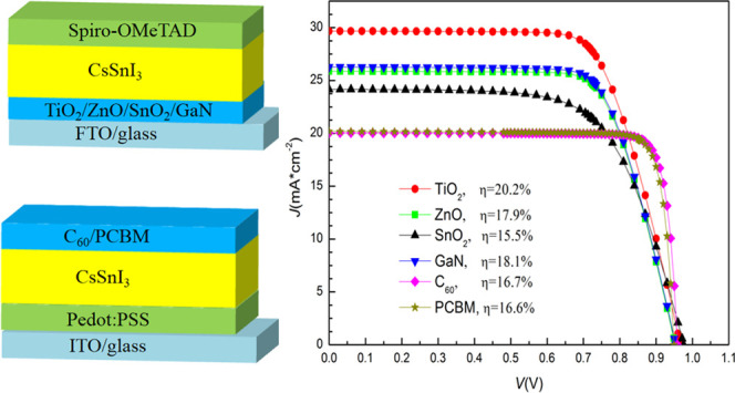
B-γ-CsSnI3 perovskite solar cells (PSCs) are simulated employing diverse electron-transporting layers (ETLs, including TiO2, ZnO, SnO2, GaN, C60, and PCBM), and a comparative study has been made. Both regular and inverted planar structures are simulated. Effects of the thickness of absorbers and ETLs, doping of ETLs, and interface trap states on the photovoltaic performance are studied to optimize the device structures. The regular structures have larger short-circuit current density (Jsc) than the inverted structures, but the inverted structures have larger fill factor (FF). All of the simulated optimal PSCs have similar open-circuit voltages (Voc) of ∼0.96 V. The PSCs with TiO2 ETLs have the best photovoltaic performance, and the optimum structure exhibits the highest efficiency of 20.2% with a Voc of 0.97 V, Jsc of 29.67 mA/cm2, and FF of 0.70. The optimal PSCs with ZnO, GaN, C60, and PCBM ETLs exhibit efficiencies of 17.88, 18.09, 16.71, and 16.59%, respectively. The optimal PSC with SnO2 ETL exhibits the lowest efficiency of 15.5% in all of the simulated PSCs due to its cliff-like band offset at the SnO2/CsSnI3 interface. Furthermore, the increase of interface trap density and capture cross section is found to reduce the photovoltaic performance of PSCs. This work contributes to designing and fabricating CsSnI3 PSCs.
1. Introduction
Perovskite solar cells (PSCs) have emerged as a breakthrough photovoltaic (PV) technology, holding unprecedented promise for high-efficiency, low-cost solar cells due to their excellent photoelectric properties.1−5 However, the potential toxicity associated with the lead-containing PSCs has become a major concern. The primary drawback of Pb perovskites for solar cells is that soluble Pb compounds are well known to be toxic to both the natural environment and humans. Therefore, there has been growing interest in the development of alternative perovskites that use Sn instead of Pb, such as CsSnI3. Tin-based halide perovskite materials have been successfully employed in lead-free perovskite solar cells. Recently, several studies have revealed that the substitution of the methylammonium cation by cesium (Cs) in the perovskite structure could significantly enhance its thermal stability.6
The B-γ-CsSnI3 perovskite has been studied comprehensively and shown to possess favorable photoelectric properties for PV application. B-γ-CsSnI3 has a direct band gap of ≈1.3 eV,6 which is suitable for solar radiation, high absorption coefficient (≈104 cm–1 in the visible region),6 and high charge-carrier mobility (∼400 cm2/(V·s) for holes).7 B-γ-CsSnI3 has low exciton binding energy (10–20 meV,6 Wannier-type excitons), so the carrier separation in CsSnI3 is easier than that in typical organic absorbers.8 In addition, several studies6,7,9 have shown that the CsSnI3 has a melting point of 451 °C, and it can be synthesized via melting–solidification, implying superior intrinsic thermal stability. By contrast, the halide perovskite analogues of MASnI3 and FASnI3 start to decompose at ≈200 °C.6 Most of the reported power conversion efficiencies (PCEs) for CsSnI3-based PSCs are between 3 and 5%.10,11 Very recently, Li et al.12 reported a PCE of 8.2% (January 2021) for CsSnI3 PSCs, and Ye et al.13 reported PCEs of 10.1 and 9.6% (March 2021). It is remarkable that the PCE of 10.1% is the highest one among all of the lead-free all-inorganic perovskite solar cells reported so far.12,13 The aforementioned considerations provide the rationale for the study of B-γ-CsSnI3 as a promising inorganic, lead-free, thermally stable perovskite for next-generation PSCs.
Dopant concentration, thickness, mobility and lifetime of carriers, surface properties, etc., of the electron-transporting layer (ETL) and hole transporting layer (HTL) and band alignment with perovskites are crucial factors for the transport of charge carriers to the front and back contacts.14 There have been many reports on HTL-free PSCs with high performance,15−18 but very few reports on ETL-free PSCs with high performance have been found till now.19 Therefore, it seems that ETLs are essential and necessary for PSCs, at least so far.19 Theoretical and simulation studies could help to gain a deep insight into the transport mechanism of ETLs20 and select the appropriate electron-transporting materials for CsSnI3 PSCs. In addition, simulations could help to find the optimal device structures and provide the theoretical possibilities of design for CsSnI3 PSCs. However, to the best of our knowledge, there has been no theoretical and simulation literature on the comparative study of electron-transporting materials for CsSnI3 PSCs so far.
In this work, B-γ-CsSnI3 is used as an all-inorganic lead-free absorber for PSCs. Several inorganic and organic semiconductors (TiO2, ZnO, SnO2, GaN, C60, and PCBM) are adopted as ETLs for CsSnI3 PSCs. A comparative study on these electron-transporting materials has been made to select the appropriate electron-transporting materials. Both regular and inverted planar structures are simulated. Effects of the thickness of CsSnI3 and ETLs and the dopant concentration of ETLs on the photovoltaic performance of PSCs are investigated to optimize the device structures for CsSnI3 PSCs and provide the theoretical possibilities of design for CsSnI3 PSCs. On the basis of comparing the photovoltaic performance of the optimal PSCs with those ETLs, the possible reasons (band structures, material, and device parameters) behind the discrepancies of performance are investigated and discussed in detail, to provide guidance for designing CsSnI3 PSCs. In addition, the effects of interface trap density of states are also studied.
2. Modeling and Simulations
The exciton in typical organic absorbers is of Frenkel-type; therefore, the exciton binding energy has to be taken into account for the carrier separation for accurate PV device modeling, which is rather complicated.8 In contrast, the exciton in the CsSnI3 perovskite is of typical Wannier-type, so the photoexcited carriers can be dealt with in the same manner as with inorganic materials. The two facts, i.e., structural similarity without the mesoporous structure and the exciton type, enable us to apply an existing device simulator widely used in inorganic solar cells to the perovskite solar cells.8
In this study, AMPS-1D software21 is used to simulate CsSnI3 PSCs. AMPS-1D is a one-dimensional device physics code and based on the basic equations of semiconductors and solar cells.21 We have successfully applied this code in the simulation of InxGa1–xN/SnS and AlxGa1–xN/SnS heterojunction solar cells.22 Here, we briefly describe the main equations used in the simulation as follows. Poisson’s equation:
| 1 |
where the local vacuum level (in the unit of eV), absolute dielectric constant and the free electron n, free hole p, trapped electron nt and trapped hole pt, as well as the ionized donor-like doping ND+ and ionized acceptor-like doping NA– concentrations are all functions of the position coordinate x. q is the electron charge. The continuity equation for electrons is as follows:
| 2 |
The continuity equation for holes is as follows:
| 3 |
 and
and  are the electron and hole current densities,
respectively. μn and μp are the
mobilities of the electron and hole, respectively. Efn and Ef are the electron and hole quasi-Fermi levels, respectively. R(x) is the net recombination rate resulting
from direct (band-to-band) recombination and indirect (Shockley–Read–Hall)
recombination traffic through gap states. GL(x) is the optical generation rate.
Determining
transport characteristics then becomes a task of solving
the three coupled nonlinear differential equations (eqs 1–3), each of which has two associated boundary conditions. In AMPS,
these three coupled equations are solved simultaneously to obtain
a set of three unknown state variables at each point in the device:
the local vacuum level and the electron and hole quasi-Fermi levels.
From these three state variables, the free carrier concentrations
( and
and  , where Nc and Nv are the effective density of states in the
conduction band and the valence band, respectively; k is the Boltzmann constant, T the temperature, and F1/2(ξ) the Fermionic integral), fields
  , currents, etc. can then be computed.
The structures of regular and inverted planar CsSnI3 PSCs are shown in Figure 1. The material parameters of CsSnI3, ETLs, and HTLs used in the simulations are shown in Table S1. The lifetime model is adopted in this work except that the density of states (DOS) model is used in the simulation of interface trap density of states. The simulation is performed under AM1.5G illumination (100 mW/cm2, 0.32–1.32 μm). Following are the simulation procedures carried out to understand the behavior and role of ETLs:
-
(a)
The band structures.
-
(b)
The effect of thickness of absorber.
-
(c)
The effect of thickness and dopant concentration of ETLs.
-
(d)
Comparison of the photovoltaic performance for the best structures.
-
(e)
The effect of interface trap density of states.
Figure 1.
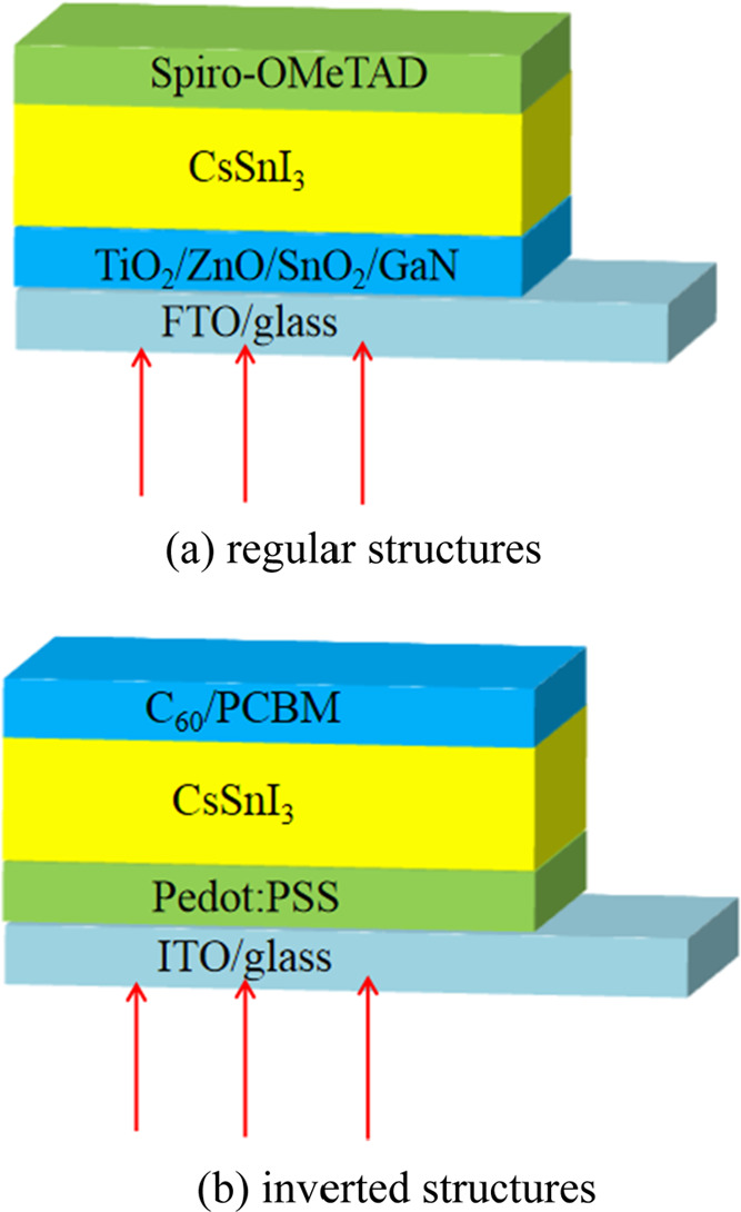
Structures of CsSnI3 perovskite solar cells.
3. Results and Discussion
3.1. Band Structures
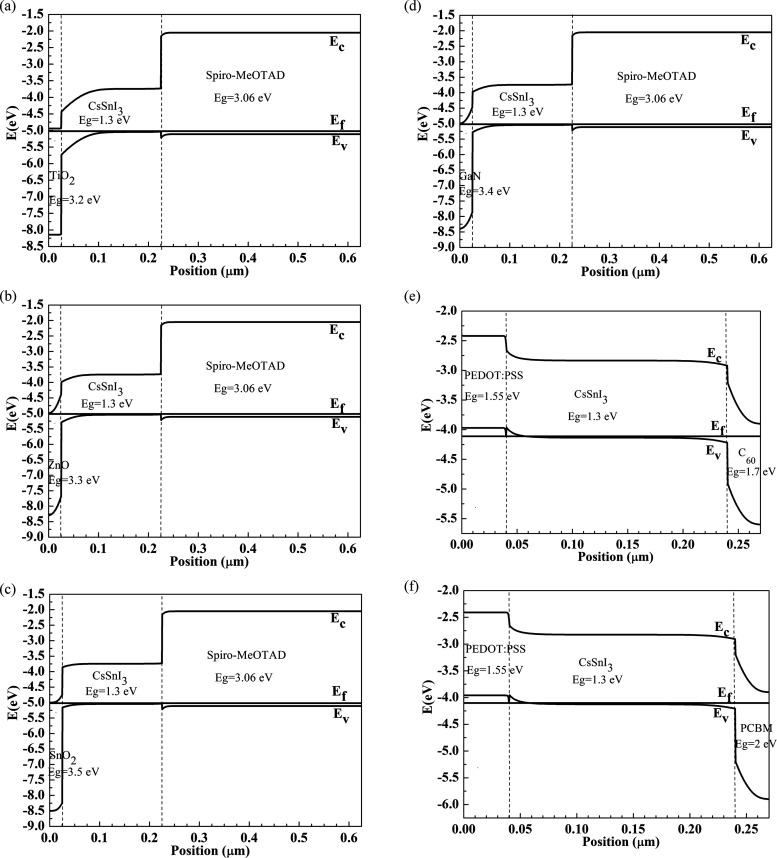
The band alignment of all contact materials and CsSnI3 adopted in this study is shown in Figure S1, and the initial thickness and donor concentrations of ETLs are shown in Table S1. The band structures of all of the simulated PSCs are shown in Figure 2. As the band gap (Eg) and electron affinity (χ) of TiO2, ZnO, and GaN are very close, the band structures of PSCs with TiO2, ZnO, and GaN are similar. For all of the simulated PSCs, there is no spike-like band offset in the conduction band at the ETL/CsSnI3 interface, which can form an electron barrier to block the drift of photogenerated electrons from CsSnI3 absorbers and lead to the degraded collection efficiency. Besides, the valence band offset at the ETL/CsSnI3 interface can generate a hole barrier to prevent the hole in CsSnI3 from moving to ETLs. However, as the electron affinity of SnO2 is too large for the PSC with SnO2, there are cliff-like band offsets in the conduction band at the SnO2/CsSnI3 interface (ΔEc = χ(CsSnI3) – χ(SnO2) = 3.62 – 4.5 = −0.88 eV, ΔEv = ΔEc + Eg(CsSnI3) – Eg(SnO2) = −0.88 + 1.3 – 3.5 = −3.08 eV), which can give rise to high interface-related recombination.23
Figure 2.
Band structures of CsSnI3 PSCs. CsSnI3 PSC with ETL TiO2 (a), ZnO (b), SnO2 (c), GaN (d), C60 (e), and PCBM (f).
3.2. Effect of the Thickness of Absorbers
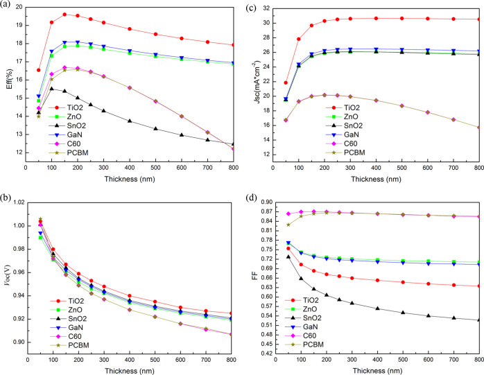
Variation of PSC performance with the thickness of CsSnI3 absorbers is shown in Figure 3. The shape of efficiency curves is similar for all of the ETLs (TiO2, ZnO, SnO2, GaN, C60, and PCBM), and the same is true for open-circuit voltages (Voc) curves and short-circuit current density (Jsc) curves. The efficiencies increase more or less steeply up to 100–200 nm and then decrease up to 800 nm (the efficiencies for SnO2, C60, and PCBM decrease sharply up to 800 nm). The PSCs with SnO2 exhibit the lowest efficiencies in all of the simulated PSCs. It is attributed to their cliff-like band offsets at the SnO2/CsSnI3 interface (see Figure 2), which give rise to high interface-related recombination and low fill factor (FF).23 When the thickness of absorbers (CsSnI3) increases, recombination in the absorbers and reverse saturated current increases. Therefore, Voc decreases with increasing CsSnI3 thickness. The regular structures have larger Jsc. The Jsc increases more or less steeply up to 100–200 nm, which is attributed to the increased optical absorption and photogenerated carriers. When the thickness of absorbers increases further (>200 nm), Jsc tends to be saturated (for the regular structures) or decreases (for the inverted structures). It is because the recombination and series resistance increases when the thickness of absorbers increases. For the regular structures, FF decreases with the increasing thickness of absorbers, which is also due to the increased recombination and series resistance. The simulated results show that the inverted structures have larger FF than the regular structures. The optimal thickness of PSCs with TiO2, ZnO, SnO2, GaN, C60, and PCBM is 150, 200, 100, 200, 150, and 200 nm, respectively. The optimal thickness of absorbers is in the range of 100–200 nm, which is consistent with some experimental reports.6,24−26 In this work, the hole mobility of 400 cm2/V/s7 was used for CsSnI3, which was obtained from transport property measurements. If the calculated hole mobility of 585 cm2/V/s7 is used, the optimal thickness of CsSnI3 absorbers should be longer. In the following sections, the thickness of CsSnI3 absorbers is set as the optimal thickness for all of the simulated PSCs.
Figure 3.
Photovoltaic performance of CsSnI3 PSCs as functions of the thickness of CsSnI3 absorbers eff (a), Voc (b), Jsc (c), and FF (d).
3.3. Effect of the Thickness and Dopant Concentrations of ETLs
Figure 4 is the plot of the efficiency and Jsc versus the thickness of ETLs. The figure shows that the efficiency and Jsc are not very sensitive to the thickness of the ETLs. For example, the efficiency of PSCs with TiO2 gradually decreases from 19.61 to 19.534% and Jsc gradually decreases from 29.689 to 29.532 mA/cm2 due to the fractional absorption of incident light by the ETLs and increase in series resistance. Voc and FF remain almost the same when the thickness of the ETLs increases. For simplicity, the thickness of the ETLs is set as 30 nm for all of the simulated PSCs.
Figure 4.
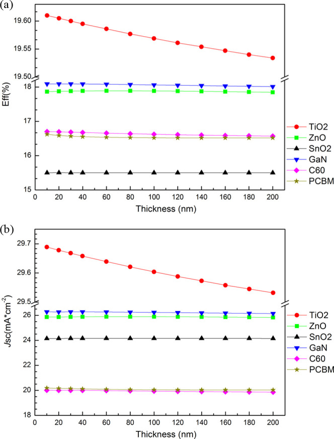
Efficiency (a) and Jsc (b) of CsSnI3 PSCs as functions of the thickness of ETLs.
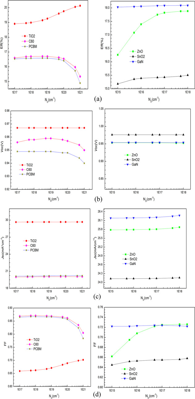
Figure 5 shows the PV cell parameters as functions of dopant concentrations (ND). In the figure, ND is set below the density of states in the conduction band of ETLs, and the barrier height of the ETL/electrode contact (qϕm = Ec – Ef) is set to make a flat band. For the regular structures, the PV parameters (efficiency, Jsc, and FF) are enhanced (slightly) with increasing dopant concentrations due to the increase in the conductivity of ETLs. For the inverted structures, the PV parameters (efficiency, Voc, and FF) increase slightly first and then decrease. The decrease of PV parameters may be attributed to the change of band structures caused by the increased dopant concentrations and has been observed in the experiment for the inverted MAPbI3 PSCs.27 In the following sections, the dopant concentrations are set as the optimal concentrations (see Table S1) for all of the simulated PSCs. For the inverted CsSnI3 PSCs, the optimal donor concentrations of ETLs are about 5 × 1018 cm–3.
Figure 5.
Photovoltaic performance of CsSnI3 PSCs as functions of dopant concentrations (ND) eff (a), Voc (b), Jsc (c), and FF (d).
3.4. Comparison of Photovoltaic Performance for the Best Structures
The best photovoltaic performance and optimal device parameters of all of the simulated PSCs are shown in Figure 6 and Table 1, respectively. From the figure and table, the regular structures have higher Jsc than the inverted structures, but the inverted structures have a larger FF. All of the simulated optimal PSCs have similar Voc. The optimal PSC with TiO2 exhibits the highest efficiency of 20.131%, and the optimal PSC with SnO2 exhibits the lowest efficiency of 15.504%. It could be concluded that there should not be spike-like or cliff-like band offsets in the conduction band at the ETL/CsSnI3 interface to obtain high performance. The band gap and electron affinity of TiO2, ZnO, and GaN are very close, but it is noted that TiO2 has a large dielectric constant of 55,28 which is much higher than that of ZnO (8.65629) and GaN (9.530). Some groups31−33 have investigated experimentally how ETLs with different dielectric constants affect the performance of organic–inorganic hybrid PSCs. They found that the dielectric constant of ETLs plays an important role in preventing electron–hole recombination in PSCs and the device performance could be improved with the increased dielectric constant of ETLs.31−33 The photovoltaic performance of PSC with C60 is slightly better than that of PSC with PCBM. It is partly attributed to the fact that the carrier mobility of C60 (1.6 cm2/V/s34) is higher than that of PCBM (0.01 cm2/V/s35).
Figure 6.
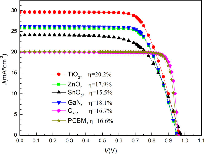
Photovoltaic performance of optimal CsSnI3 PSCs.
Table 1. Best Photovoltaic Performance and Optimal Device Parameters of CsSnI3 PSCs.
| PSC with ETL | TiO2 | ZnO | SnO2 | GaN | C60 | PCBM |
|---|---|---|---|---|---|---|
| thickness of CsSnI3 absorber (nm) | 150 | 200 | 100 | 200 | 150 | 200 |
| thickness of ETL (nm) | 30 | 30 | 30 | 30 | 30 | 30 |
| donor concentration ND (cm–3) | 1.00 × 10²¹ | 1.00 × 10¹⁸ | 1.00 × 10¹⁸ | 1.00 × 10¹⁸ | 5.00 × 10¹⁸ | 5.00 × 10¹⁸ |
| eff (%) | 20.131 | 17.882 | 15.504 | 18.091 | 16.711 | 16.589 |
| Voc (V) | 0.967 | 0.952 | 0.976 | 0.954 | 0.959 | 0.949 |
| Jsc (mA/cm2) | 29.673 | 25.874 | 24.158 | 26.273 | 20.037 | 20.177 |
| FF | 0.702 | 0.726 | 0.658 | 0.722 | 0.87 | 0.866 |
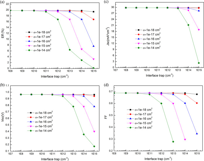
All of the simulated optimal PSCs with diverse electron-transporting materials (both regular and inverted planar structures) exhibit a similar Voc of ∼0.96 V. However, in practice, low Voc (<0.6 V) was reported in most of the experimental CsSnI3 PSCs,36−38 which is far behind the band gap (1.3 eV) of CsSnI3 absorbers. For comparison, the Voc exceeding 1.26 V could be achieved with its band gap of 1.55 eV for MAPbI3 PSCs.39 In the research field of CsSnI3 PSCs, the most crucial goal is to develop efficient strategy to improve Voc of the devices, and more fundamental studies are required to understand the origin of low Voc.38 It can be seen from Figure 9b that the interface trap at the ETLs/CsSnI3 interface could cause a significant drop in Voc when the interface trap density and capture cross section are large. From the simulation results and other experimental reports,12,13,38 it could be concluded that the low crystal quality of CsSnI3 thin films and the interface quality may mainly be responsible for the low Voc in CsSnI3 PSCs. Defects in the CsSnI3 films and interface trap could increase recombination and reverse saturation current, and thus reduce Voc. Li et al.12 reported (January 2021) that an obvious Voc enhancement from 0.47 to 0.63 V is achieved by reducing deep level trap-state density with the surface passivation of thiosemicarbazide. Ye et al.13 (March 2021) found that the undesirable oxidation in CsSnI3 is restricted by engineering the localized electron density with a phthalimide (PTM) additive and demonstrated that the lone electron pairs of NH and two CO functional groups in the PTM form coordination interactions with Sn2+ in the CsSnI3 and protect it from oxidation to Sn4+. Their CsSnI3-PTM device exhibited an overall PCE of 10.1% with a Voc of 0.64 V.
Figure 9.
Photovoltaic performance of TiO2/CsSnI3/Spiro-OMeTAD PSCs as functions of the interface trap density and capture cross section eff (a), Voc (b), Jsc (c), and FF (d).
The quantum efficiencies (QEs) or spectral responses of all of the simulated PSCs are shown in Figure 7. In the near-infrared region, the quantum efficiencies of the PSCs decrease sharply at about 950 nm, which corresponds to the band gap of CsSnI3 thin film. PSC with TiO2 exhibits the highest quantum efficiency (∼0.88) in the visible region. The inverted structures with C60 and PCBM exhibit the lowest quantum efficiency (∼0.59) in the visible region and thus the lowest Jsc.
Figure 7.
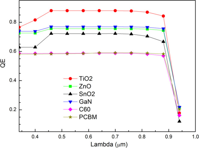
Quantum efficiencies of optimal CsSnI3 PSCs.
Figure 8 shows the quantum efficiencies of TiO2/CsSnI3/Spiro-OMeTAD PSCs versus the thickness of CsSnI3 absorbers. The quantum efficiencies increase steeply when the thickness of the absorber increases from 50 to 100 nm due to the increased optical absorption and photogenerated carriers. It tends to be saturated when the thickness of the absorber increases above 200 nm, which is because the recombination increases (so the collection efficiency decreases) and series resistance increases. When the thickness of CsSnI3 is 150 nm, the optimal TiO2/CsSnI3/Spiro-OMeTAD PSC exhibits the highest efficiency of 20.131% (Jsc = 29.673 mA/cm2).
Figure 8.
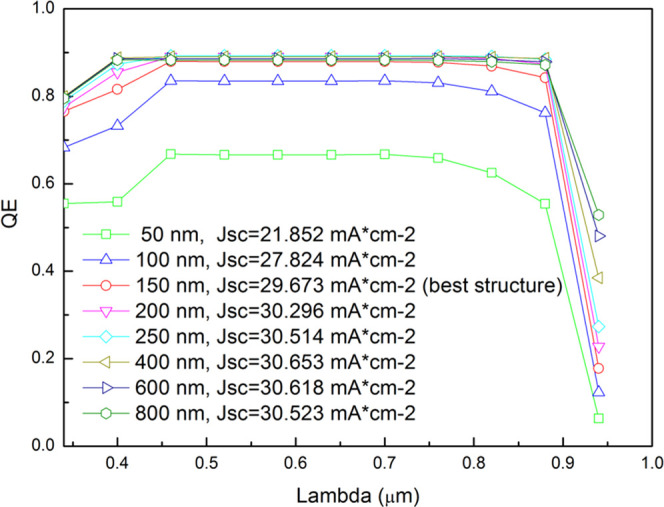
Quantum efficiencies of TiO2/CsSnI3/Spiro-OMeTAD PSCs versus the thickness of CsSnI3 absorbers.
3.5. Effect of the Interface Trap Density of States
The nanoscale interface states play an important role in the device performance.40 In the device simulation, the effects of the interface trap density of states are also studied by introducing a 5 nm interface defect layer (IDL) at the TiO2/CsSnI3 interface for TiO2/CsSnI3/Spiro-OMeTAD PSCs. Figure 9 shows the plot of PV cell parameters as functions of the interface trap density and capture cross section. From the figure, the interface trap has an important influence on efficiency, Voc, Jsc, and FF. It is clear that efficiency, Voc, Jsc, and FF decrease with increasing interface trap density and capture cross section. When the capture cross sections are 10–18 and 10–17 cm2, the efficiencies decrease slowly from 19.825 to 19.424% and 16.798%, respectively. However, when the capture cross section increases to 10–15 and 10–14 cm2, the efficiency decreases sharply to 3.232 and 0.154%, respectively. Interface trap and large capture cross section increase the recombination centers and hence change in shunt resistance. Optimizing the doping of the ETL and formation of a flat, smooth, and homogeneous surface will significantly reduce the interface trap density and hence enhance the performance. The recombination mechanisms of photocarriers at the ETL/perovskite interfaces could be found in the literature, such as refs41, 42.
4. Conclusions
B-γ-CsSnI3 has attracted considerable attention as a promising inorganic, lead-free, thermally stable perovskite for next-generation PSCs due to its favorable photoelectric properties. In this work, CsSnI3 PSCs with diverse ETLs (TiO2, ZnO, SnO2, GaN, C60, and PCBM) were simulated. Effects of the thickness of CsSnI3 absorbers and ETLs, dopant concentration of ETLs, and interface trap density of states on the photovoltaic performance of PSCs were investigated to find the optimal device structures. The optimal thickness of CsSnI3 absorbers is in the range of 100–200 nm (the hole mobility of 400 cm2/V/s7 was used for CsSnI3, which was obtained from transport property measurements). The regular structures have larger Jsc than the inverted structures, but the inverted structures have larger FF. All of the simulated optimal PSCs exhibit a similar Voc of ∼0.96 V.
It was found that the photovoltaic performance of CsSnI3 PSCs is not very sensitive to the thickness of the ETLs. The optimal thickness of ETLs is about 20–30 nm. For the regular structures, the PV parameters (efficiency, Jsc, and FF) are enhanced (slightly) with increasing dopant concentrations of ETLs due to the increase in the conductivity of ETLs. For the inverted structures, the PV parameters (efficiency, Voc, and FF) increase slightly first and then decrease with increasing dopant concentrations of ETLs. The optimal donor concentrations of ETLs are about 5 × 1018 cm–3 for the inverted structures. It was found that TiO2 is the best electron-transporting material in all of the simulated ETLs. When the thickness of CsSnI3 is 150 nm, the optimal TiO2/CsSnI3/Spiro-OMeTAD PSC exhibits the highest efficiency of 20.2% with a Voc of 0.97 V, Jsc of 29.67 mA/cm2, and FF of 0.70. The optimal PSCs with ZnO, GaN, C60, and PCBM ETLs exhibit efficiencies of 17.88, 18.09, 16.71, and 16.59%, respectively. The optimal PSC with SnO2 ETL exhibits the lowest efficiency of 15.5% in all of the simulated PSCs due to its cliff-like band offset at the SnO2/CsSnI3 interface. It could be concluded that there should not be spike-like or cliff-like band offsets in the conduction band at the ETL/CsSnI3 interface to obtain high performance. Furthermore, the photovoltaic performance of PSCs was found to degrade with increasing interface trap density and capture cross section.
Acknowledgments
This work is supported by the Xiamen University Malaysia Research Fund (No. XMUMRF/2019-C3/IORI/0001), the Education Department of Fujian Province JK Project (No. JK2017033), Minnan Normal University Project (Nos. HX2019077 and XJZ18046), National Natural Science Foundation of China (No. 61975072), Industry-University-Research Collaboration Foundation of the Fujian Province (No. 2020H6017), and Program for Innovative Research Team in Science and Technology in Fujian Province University (Optoelectronic Materials and Device Application). The authors would like to thank the Fonash Research Group in the Pennsylvania State University for providing the AMPS-1D simulation package.
Supporting Information Available
The Supporting Information is available free of charge at https://pubs.acs.org/doi/10.1021/acsomega.1c04096.
Material parameters of CsSnI3, ETLs, and HTLs used in the simulations (Table S1) and band alignment of all contact materials and CsSnI3 adopted in this study (Figure S1) (PDF)
Author Contributions
The manuscript was written through the contributions of all authors. All authors have given approval to the final version of the manuscript.
The authors declare no competing financial interest.
Supplementary Material
References
- Lee M. M.; Teuscher J.; Miyasaka T.; Murakami T. N.; Snaith H. J. Efficient hybrid solar cells based on meso-superstructured organometal halide perovskites. Science 2012, 338, 643–647. 10.1126/science.1228604. [DOI] [PubMed] [Google Scholar]
- Jeong J.; Kim M.; Seo J.; Lu H.; Ahlawat P.; Mishra A.; Yang Y.; Hope M. A.; Eickemeyer F. T.; Kim M.; Yoon Y. J.; Choi I. W.; Darwich B. P.; Choi S. J.; Jo Y.; Lee J. H.; Walker B.; Zakeeruddin S. M.; Emsley L.; Rothlisberger U.; Hagfeldt A.; Kim D. S.; Grätzel M.; Kim J. Y. Pseudo-halide anion engineering for α-FAPbI3 perovskite solar cells. Nature 2021, 592, 381–385. 10.1038/s41586-021-03406-5. [DOI] [PubMed] [Google Scholar]
- Ishikawa R.; Watanabe S.; Yamazaki S.; Oya T.; Tsuboi N. Perovskite/graphene solar cells without a hole-transport layer. ACS Appl. Energy Mater. 2019, 2, 171–175. 10.1021/acsaem.8b01606. [DOI] [Google Scholar]
- Tessler N.; Vaynzof Y. Preventing hysteresis in perovskite solar cells by undoped charge blocking layers. ACS Appl. Energy Mater. 2018, 1, 676–683. 10.1021/acsaem.7b00176. [DOI] [Google Scholar]
- Shalenov E. O.; Dzhumagulova K. N.; Seitkozhanov Y. S.; Ng A.; Valagiannopoulos C.; Jumabekov A. N. Insights on desired fabrication factors from modeling sandwich and quasi-interdigitated back-contact perovskite solar cells. ACS Appl. Energy Mater. 2021, 4, 1093–1107. 10.1021/acsaem.0c02120. [DOI] [Google Scholar]
- Wang N.; Zhou Y.; Ju M.; Garces H. F.; Ding T.; Pang S.; Zeng X. C.; Padture N. P.; Sun X. W. Heterojunction-depleted lead-free perovskite solar cells with coarse-grained B-γ-CsSnI3 thin films. Adv. Energy Mater. 2016, 6, 1670137 10.1002/aenm.201670137. [DOI] [Google Scholar]
- Chung I.; Song J. H.; Im J.; Androulakis J.; Malliakas C. D.; Li H.; Freeman A. J.; Kenney J. T.; Kanatzidis M. G. CsSnI3: semiconductor or metal? High electrical conductivity and strong near-infrared photoluminescence from a single material. High hole mobility and phase-transitions. J. Am. Chem. Soc. 2012, 134, 8579–8587. 10.1021/ja301539s. [DOI] [PubMed] [Google Scholar]
- Minemoto T.; Murata M. Device modeling of perovskite solar cells based on structural similarity with thin film inorganic semiconductor solar cells. J. Appl. Phys. 2014, 116, 054505 10.1063/1.4891982. [DOI] [Google Scholar]
- Chung I.; Lee B.; He J.; Chang R. P. H.; Kanatzidis M. G. All-solid-state dye-sensitized solar cells with high efficiency. Nature 2012, 485, 486–489. 10.1038/nature11067. [DOI] [PubMed] [Google Scholar]
- Ma S.; Gu X.; Kyaw A. K.; Wang D. H.; Priya S.; Ye T. Fully Inorganic CsSnI3-based solar cells with>6% efficiency and enhanced stability enabled by mixed electron transport layer. ACS Appl. Mater. Interfaces 2021, 13, 1345–1352. 10.1021/acsami.0c16634. [DOI] [PubMed] [Google Scholar]
- Wang Y.; Tu J.; Li T.; Tao C.; Deng X.; Li Z. Convenient preparation of CsSnI3 quantum dots, excellent stability, and the highest performance of lead-free inorganic perovskite solar cells so far. J. Mater. Chem. A 2019, 7, 7683–7690. 10.1039/C8TA10901J. [DOI] [Google Scholar]
- Li B.; Di H.; Chang B.; Yin R.; Fu L.; Zhang Y.; Yin L. Efficient passivation strategy on Sn related defects for high performance all-inorganic CsSnI3 perovskite solar cells. Adv. Funct. Mater. 2021, 31, 2007447 10.1002/adfm.202007447. [DOI] [Google Scholar]
- Ye T.; Wang X.; Wang K.; Ma S.; Yang D.; Hou Y.; Yoon J.; Wang K.; Priya S. Localized electron density engineering for stabilized B-γ CsSnI3-based perovskite solar cells with efficiencies >10%. ACS Energy Lett. 2021, 6, 1480–1489. 10.1021/acsenergylett.1c00342. [DOI] [Google Scholar]
- Adhikari K. R.; Gurung S.; Bhattarai B. K.; Soucase B. M. Comparative study on MAPbI3 based solar cells using different electron transporting materials. Phys. Status Solidi C 2016, 13, 13–17. 10.1002/pssc.201510078. [DOI] [Google Scholar]
- Etgar L.; Gao P.; Xue Z. S.; Peng Q.; Chandiran A. K.; Liu B.; Nazeeruddin M. K.; Grätzel M. Mesoscopic CH3NH3PbI3/TiO2 heterojunction solar cells. J. Am. Chem. Soc. 2012, 134, 17396–17399. 10.1021/ja307789s. [DOI] [PubMed] [Google Scholar]
- Laban W. A.; Etgar L. Depleted hole conductor-free lead halide iodide heterojunction solar cells. Energy Environ. Sci. 2013, 6, 3249–3253. 10.1039/c3ee42282h. [DOI] [Google Scholar]
- Aharon S.; Gamliel S.; El Cohen B.; Etgar L. Depletion region effect of highly efficient hole conductor free CH3NH3PbI3 perovskite solar cells. Phys. Chem. Chem. Phys. 2014, 16, 10512–10518. 10.1039/C4CP00460D. [DOI] [PubMed] [Google Scholar]
- Aharon S.; El Cohen B.; Etgar L. Hybrid lead halide iodide and lead halide bromide in efficient hole conductor free perovskite solar cell. J. Phys. Chem. C 2014, 118, 17160–17165. 10.1021/jp5023407. [DOI] [PubMed] [Google Scholar]
- Xiao L. X.; Zou D. C.. Perovskite Solar Cells, 2nd ed.; Peking University Press, 2020. [Google Scholar]
- Chen J. Y.; Chen F. X.; Xu W. K.; Cao G. H.; Wang L. S. Simulation optimization of planar heterojunction perovskite solar cells with B-γ-CsSnI3 as optical absorption layer. J. Synth. Cryst. 2018, 47, 31–36. [Google Scholar]
- Fonash S. J.et al. AMPS Manual, 2010. http://www.ampsmodeling.org/pdfs/AMPS-1D%20Manual.pdf.
- Lin S.; Li X. R.; Pan H. Q.; Chen H. T.; Li X. Y.; Li Y.; Zhou J. R. Numerical analysis of InxGa1-xN/SnS and AlxGa1-xN/SnS heterojunction solar cells. Energy Convers. Manage. 2016, 119, 361–367. 10.1016/j.enconman.2016.04.059. [DOI] [Google Scholar]
- Ghorbani E. On efficiency of earth-abundant chalcogenide photovoltaic materials buffered with CdS: the limiting effect of band alignment. J. Phys.: Energy 2020, 2, 025002 10.1088/2515-7655/ab6942. [DOI] [Google Scholar]
- Marshall K. P.; Walton R. I.; Hatton R. A. Tin perovskite/fullerene planar layer photovoltaics: improving the efficiency and stability of lead-free devices. J. Mater. Chem. A 2015, 3, 11631–11640. 10.1039/C5TA02950C. [DOI] [Google Scholar]
- Marshall K. P.; Walker M.; Walton R. I.; Hatton R. A. Enhanced stability and efficiency in hole-transport-layer-free CsSnI3 perovskite photovoltaics. Nat. Energy 2016, 1, 16178 10.1038/nenergy.2016.178. [DOI] [Google Scholar]
- Wu B.; Zhou Y.; Xing G.; Xu Q.; Garces H. F.; Solanki A.; Goh T. W.; Padture N. P.; Sum T. C. Long minority-carrier diffusion length and low surface-recombination velocity in inorganic lead-free CsSnI3 perovskite crystal for solar cells. Adv. Funct. Mater. 2017, 27, 1604818 10.1002/adfm.201604818. [DOI] [Google Scholar]
- Bin Z.; Li J.; Wang L.; Duan L. Efficient n-type dopants with extremely low doping ratios for high performance inverted perovskite solar cells. Energy Environ. Sci. 2016, 9, 3424–3428. 10.1039/C6EE01987K. [DOI] [Google Scholar]
- vande Krol R.; Goossens A.; Schoonman J. Mott-Schottky analysis of nanometer-scale thin-film anatase TiO2. J. Electrochem. Soc. 1997, 144, 1723–1727. 10.1149/1.1837668. [DOI] [Google Scholar]
- Pearton S. J.; Norton D. P.; Ip K.; Heo Y. W.; Steiner T. Recent progress in processing and properties of ZnO. Superlattices Microstruct. 2003, 34, 3–32. 10.1016/S0749-6036(03)00093-4. [DOI] [Google Scholar]
- Lin S.; Zeng S. W.; Cai X. M.; Zhang J. Y.; Wu S. X.; Sun L.; Zhang B. P. Simulation of doping levels and deep levels in InGaN-based single-junction solar cell. J. Mater. Sci. 2012, 47, 4595–4603. 10.1007/s10853-012-6321-6. [DOI] [Google Scholar]
- Shao S.; Abdu-Aguye M.; Qiu L.; Lai L. H.; Liu J.; Adjokatse S.; Jahani F.; Kamminga M. E.; ten Brink G. H.; Palstra T. T. M.; Kooi B. J.; Hummelenab J. C.; Loi M. A. Elimination of the light soaking effect and performance enhancement in perovskite solar cells using a fullerene derivative. Energy Environ. Sci. 2016, 9, 2444–2452. 10.1039/C6EE01337F. [DOI] [Google Scholar]
- Castro E.; Fernandez-Delgado O.; Arslan F.; Zavala G.; Yang T.; Seetharaman S.; D’Souza F.; Echegoyen L. New thiophene-based C60 fullerene derivatives as efficient electron transporting materials for perovskite solar cells. New J. Chem. 2018, 42, 14551–14558. 10.1039/C8NJ03067G. [DOI] [PMC free article] [PubMed] [Google Scholar]
- Shao S.; Liu J.; Fang H. H.; Qiu L.; ten Brink G. H.; Hummelen J. C.; Koster L. J. A.; Loi M. A. Efficient perovskite solar cells over a broad temperature window: the role of the charge carrier extraction. Adv. Energy Mater. 2017, 7, 1701305 10.1002/aenm.201701305. [DOI] [Google Scholar]
- Golubev T.; Liu D.; Lunt R.; Duxbury P. Understanding the impact of C60 at the interface of perovskite solar cells via drift-diffusion modeling. AIP Adv. 2019, 9, 035026 10.1063/1.5068690. [DOI] [Google Scholar]
- Zhao P.; Liu Z.; Lin Z.; Chen D.; Su J.; Zhang C.; Zhang J.; Chang J.; Hao Y. Device simulation of inverted CH3NH3PbI3–xClx perovskite solar cells based on PCBM electron transport layer and NiO hole transport layer. Sol. Energy 2018, 169, 11–18. 10.1016/j.solener.2018.04.027. [DOI] [Google Scholar]
- Tai Q.; Tang K.-C.; Yan F. Recent progress of inorganic perovskite solar cells. Energy Environ. Sci. 2019, 12, 2375–2405. 10.1039/C9EE01479A. [DOI] [Google Scholar]
- Konstantakou M.; Stergiopoulos T. A critical review on tin halide perovskite solar cells. J. Mater. Chem. A 2017, 5, 11518–11549. 10.1039/C7TA00929A. [DOI] [Google Scholar]
- Gao W.; Li P.; Chen J.; Ran C.; Wu Z. Interface engineering in tin perovskite solar cells. Adv. Mater. Interfaces 2019, 6, 1901322 10.1002/admi.201901322. [DOI] [Google Scholar]
- Liu Z.; Krückemeier L.; Krogmeier B.; Klingebiel B.; Márquez J. A.; Levcenko S.; Öz S.; Mathur S.; Rau U.; Unold T.; Kirchartz T. Open-circuit voltages exceeding 1.26 V in planar methylammonium lead iodide perovskite solar cells. ACS Energy Lett. 2019, 4, 110–117. 10.1021/acsenergylett.8b01906. [DOI] [Google Scholar]
- Wang H.-Q.; Xu J.; Lin X.; Li Y.; Kang J.; Zheng J.-C. Determination of the embedded electronic states at nanoscale interface via surface-sensitive photoemission spectroscopy. Light: Sci. Appl. 2021, 10, 153 10.1038/s41377-021-00592-9. [DOI] [PMC free article] [PubMed] [Google Scholar]
- Le Corre V. M.; Stolterfoht M.; Toro L. P.; Feuerstein M.; Wolff C.; Gil-Escrig L.; Bolink H. J.; Neher D.; Koster L. J. A. Charge transport layers limiting the efficiency of perovskite solar cells: how to optimize conductivity, doping, and thickness. ACS Appl. Energy Mater. 2019, 2, 6280–6287. 10.1021/acsaem.9b00856. [DOI] [Google Scholar]
- Hu J.; Gouda L.; Kama A.; Tirosh S.; Gottesman R. Radiative recombination changes under light-soaking in CsPbBr3 films on TiO2 and insulating glass contacts: interface versus bulk effects. ACS Appl. Energy Mater. 2019, 2, 3013–3016. 10.1021/acsaem.9b00335. [DOI] [Google Scholar]
Associated Data
This section collects any data citations, data availability statements, or supplementary materials included in this article.


