

Abstract
A multi-channel, CMOS-based biopotential acquisition system is presented that uses amplitude modulated, frequency division multiplexing (AM-FDM) to decrease wire count and provide resilience against motion artifacts and cable noise. Differential active electrode (AE) pairs capture surface biopotential signals, each modulated by a different carrier frequency and combined via current-domain summing. The presented approach requires only a single wire for signal transmission between AEs and back-end readout, along with clock and ground wires, to support multiple active electrodes using a 3-wire cable. Frequency modulation prior to transmission mitigates the effect of low-frequency cable motion artifacts and 50/60 Hz mains interference in the cable. A prototype FDM-based biopotential acquisition system was implemented in a 180nm CMOS process, including a four-channel front-end active electrode IC for signal conditioning and modulation, and a back-end IC for demodulation and digitization. Each channel occupies 0.75mm2 and consumes 43.8µW, inclusive of ADC power. Using both AE and BE ICs, a fourchannel biopotential recording system is demonstrated using a 3-wire interface, where the system achieves attenuation of low-frequency cable motion artifacts by 15X and 60 Hz mains noise coupled into the cable by 62X.
Keywords: Multi-channel biopotential recording, frequency-division multiplexing (FDM), electromyography (EMG), electrocardiography (ECG), gesture recognition, ExG
I. Introduction
BIOPOTENTIAL readout systems using non-invasive electrodes can indirectly record bioelectrical signals, such as multi-electrode electromyography (EMG), electrocardiography (ECG), or electroencephalography (EEG) for a variety health monitoring, diagnostic, clinical research, and brain-computer-interfaces (BCI) applications [1]–[3]. Multi-channel acquisition enhances spatial accuracy and provides additional physiological information. For instance, a 12- or 24-lead ECG system is generally used for diagnosis of cardiovascular disease [4], [5], and in recent years, multi-channel ECG measuring systems with more than 24 leads have been developed to obtain increasingly in-depth information of cardiac activity [6]. Similarly, in both intramuscular and surface EMG technologies, multi-channel EMG recording provides a rich information stream for EMG decomposition [7], [8]. However, adding more channels inherently increases the number of cables that connect from body-worn electrodes to back-end readout electronics, which not only impede ambulatory use but may also be physically limited by size, weight, and cost limitations of the wire bundle. Additionally, electrode cables are subject to motion artifacts that can corrupt the recorded signal, as well as 50/60 Hz interference injected into the cable, which occurs in the same low-frequency bandwidth as many biopotential signals (~1 Hz−150 Hz) and with comparable micro-volt signal amplitude. For example, motion artifacts introduced into long-term (1–24 hours or longer) ExG recordings in children and infants [9], [10] are a critical bottleneck that limit overall system performance.
To mitigate noise introduced in the cables connecting electrodes to readout instrumentation, first-stage amplification can be performed at the electrode site. In such an active electrode (AE) arrangement, as shown in Fig. 1a, a front-end instrumentation amplifier (IA) [11], [12] is located close to the electrodes. A high gain amplifier (>40dB) is typically required in each AE to reduce the relative effect of downstream cable motion artifacts and other cable noise sources. This one-to-one AE approach, however, still requires a large number of cables, and several additional approaches have been developed to decrease the size of the required cable bundle.
Fig. 1.

Block diagram of differential N-channel biopotential acquisition system topologies: (a) conventional active electrodes (AEs) with one wire per AE channel, and (b) FDM-based active electrodes (AEs) that share two wires for multiple AE channels.
Digital active electrodes (DAE) provide near-electrode analog-to-digital conversion and all-digital communicating with back-end (BE) readout instrumentation, minimizing cable count and providing high noise immunity [13]. However, this introduces a significant increase in power and area for each active electrode, where each DAE includes an IA, a low-pass filter (LPF), an analog-to-digital converter (ADC), and a digital communication interface. Alternatively, frequency-division multiplexing (FDM) can be used with frequency modulation (FM-FDM) as presented in [14], which reduces both the required number of ADCs and the required number of cables. As a trade-off, this approach does require off-chip inductors, but in doing so achieves low VCO phase noise and to meet required band-pass amplifier response, both helping to mitigate crosstalk.
In this work, we present an alternative approach leveraging amplitude-modulated FDM (AM-FDM) to build a highly scalable biopotential acquisition architecture towards the future development high-density ExG readout platforms. As illustrated in Fig. 1b, this approach combines multiple input signals on a single wire by modulating them at different frequencies, where up-conversion via amplitude modulation also separates the signals from low-frequency cable noise artifacts, including both motion artifacts and noise injection from mains interference (50/60 Hz). In addition, back-end signal demodulation prior to digitization enables the use of a lower-speed ADC and simplified filtering, and unlike direct time-division multiplexing (TDM) of the electrodes, all signals are sent simultaneously over a three-wire (data, clock, and ground) cable bundle without requiring an AE-side switch matrix.
The remainder of this paper is organized as follows: Section II introduces the proposed system architecture; Section III and IV describe the circuit implementation of the active electrode integrated circuit (AE-IC) and the back-end integrated circuit (BE-IC) in detail; Section V presents experimental measurement results from a fabricated prototype IC and provides brief discussion and detailed comparison with state-of-the-art approaches; and, Section VI concludes the paper.
II. FDM-based Four-Channel EMG Acquisition System Overview
A. System Overview
An overview of the proposed FDM-based bioelectrical readout system is shown in Fig. 2, where multi-channel electromyography (EMG) is used as an example application. Four AE channels are integrated in a single front-end die and powered by a battery. Each differential surface electrode pair connects to an AE through short (centimeter-scale) wires. The summed current output of the modulated, four-channel AE-IC is connected to input of the BE-IC through a single, long wire (meter scale), with two additional wires carrying ground and a shared reference clock. Up-conversion mitigates low-frequency motion artifacts, as well as 50/60 Hz mains interference injected into the connecting cables; up-conversion via amplitude modulation provides resilience to artifacts acquired after the AE IC, but not before. The BE-IC performs current-to-voltage conversion, frequency demodulation, and on-chip digitization. A final, off-chip digital signal processing (DSP) includes finite impulse response (FIR) low-pass filtering for out of band suppression and signal reconstruction. And the DSP architecture was simulated in MATLAB.
Fig. 2.

High-level architecture of the four-channel, FDM-based EMG biopotential readout system. By combining modulated signals at the front-end, 2N+1=9 AE wires can be kept short, and only three longer communication wires (clock, data, ground) from front-end to back-end are required. In additional to cable reduction, up-conversion prior to transmission also mitigates low-frequency motion artifacts and 50/60 Hz noise injected into the longer cables.
This FDM-based approach needs only three communication wires: a single data line for frequency-modulated, summed, current-mode electrode signals; a reference clock for the modulation up-mixer in the AE-IC and the demodulation down-mixer in the BE-IC, generated from an internal relaxation RC oscillator in BE-IC; and, a shared common ground between AE and BE. As the number of electrode channels increases, the required number of wires remains the same.
B. Dynamic Range and Bandwidth Considerations
While scalable, two practical factors of this system will limit the maximum number of adjacent signal channels, as is common for FDM-based systems; input dynamic range and overall bandwidth requirements.
The input dynamic range (DR) of the back-end TIA must be large enough to support the combined FDM signal voltage, where the summed, amplitude-modulated signals can together saturate the maximum voltage range, limited by the TIA maximum input current and gain, Vmax, and expressed as the following:
| (1) |
| (2) |
where Ich is the output current of a single channel, αTIA is the current-to-voltage gain of the TIA, Vmax is the maximum TIA input voltage, and N is the maximum number of channels. As such, if αTIA decreases, N can be increased, for a fixed input Vmax. However, this decreased gain can degrade measurement accuracy, where the relative noise contribution is larger due to a decreased signal LSB.
The total number of supported channels is also limited in the frequency domain by overall system bandwidth, channel bandwidth, guard-band spacing between channel bands, and the presence of harmonic overtones. As illustrated in Fig. 3, the lowest frequency harmonic to limit usable FDM bandwidth is the third harmonic of the lowest frequency modulation signal; the highest modulation frequency should be lower than this lowest third harmonic to avoid overlapping a signal channel, and the following criteria needs to be satisfied:
| (3) |
| (4) |
where fch1 and fchN are the lowest and highest modulation frequencies, BWSIG is the signal bandwidth, and BWGB is a guard band, or dead zone between modulated channels, to avoid signal overlapping into adjacent channels. (2×BWSIG + BWGB) indicates channel interval in Fig. 3.
Fig. 3.

Conceptual diagram of the frequency modulated signals.
Overall, equations (2) and (4) drive design trade-offs, where fch1 and αTIA are determined by the required number of channels and the signal characteristics. Of these, (2) will first limit channel count in the demonstrated system due to the supply-limited voltage DR. The AE includes fixed 50X LNA gain, 500nS Gm amplifier gain, 1.8 V power supply rail, and a fixed αTIA gain where the implemented RFB is 2MΩ. Assuming that the peak input voltage is less than 2.5 mV, the voltage DR will support a maximum of 14-channels as implemented. This could be further increased in future designs using programmable gain settings throughout the signal chain.
III. Active Electrode Integrated Circuit (AE-IC)
A. Overview
The architecture of the active electrode IC is shown in Fig. 4. A battery-powered AE-IC supports four active electrode channels, where each AE channel contains a low-noise amplifier (LNA) with duty-cycled resistive feedback used as an instrumentation amplifier (IA), a spike filter, a mixer to provide amplitude modulation, and a transconductor to enable channel combining in the current domain. An RC relaxation oscillator generates a reference clock for the duty-cycle resistor (DCR) in the IA, and the clock frequency can be controlled by an external resistor, REXT. Using the reference clock, a pulse generator generates a pulse with a programmable duty cycle. To increase test flexibility and limit harmonic overlap in the DCR and mixer, a local oscillator is included for each channel.
Fig. 4.
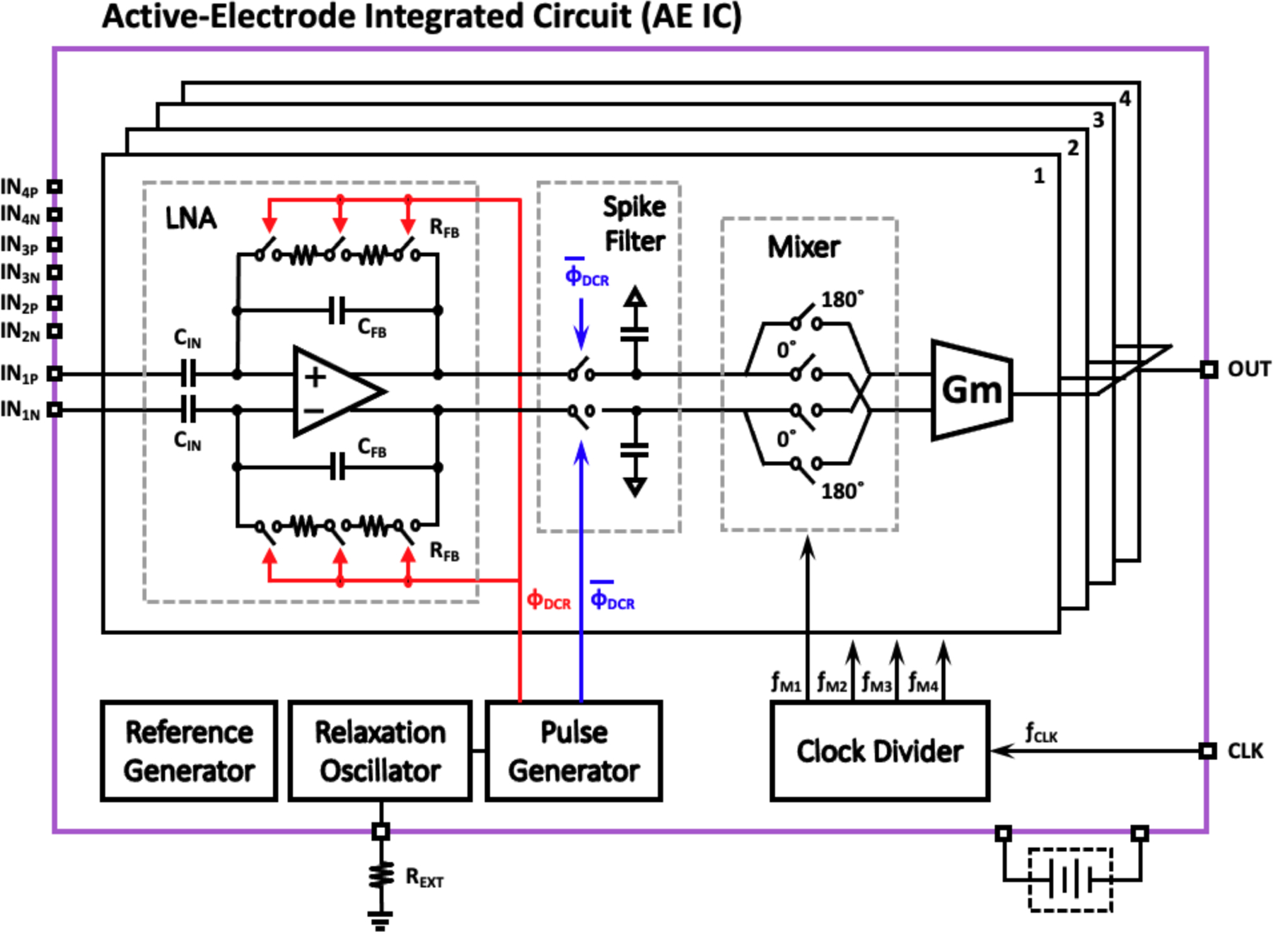
Block diagram of four-channel active electrode integrated circuit (AE-IC) used for electrode readout, up-conversion, and summing of modulated signal currents into a single, shared wire using FDM.
B. Capacitively-coupled Instrumentation Amplifier
As illustrated in Fig. 4, a capacitively-coupled instrumentation amplifier (CCIA) serves as the input stage for each active electrode channel. Capacitive coupling enables rail-to-rail offset rejection. The gain of CCIA is determined by the ratio the input capacitor (CIN) and the feedback capacitor (CFB). In addition, to attain a low corner frequency (~1 Hz) in this architecture, a large feedback capacitor (CFB) and a large resistor (RFB) are typically required. However, it is not practical to increase CFB and CIN in a limited circuit area while maintaining the required gain. To address this challenge, several architectures have been developed to achieve a very large RFB with limited circuit area. An active pseudo-resistor, using diode connected MOSFET transistors, is often employed to implement very large (≫100MΩ) on-chip resistance [15]. However, pseudo-resistors provide linear behavior only for very small signals. Alternatively, a duty-cycled switched resistor (DCR) can be used to improve linearity and reliability across a larger signal range [16]. However, the DCR switch parasitic capacitance, Cp, may limit saturated maximum resistance to R = 1/(f1Cp) [17]. In this work, we instead use a cascaded multi-switching duty-cycle resistor (MS-DCR) [18] to mitigate this limitation.
For the active electrode, the CCIA is the primary noise contributor for the signal chain, as the input-referred noise of each following block is divided by the CCIA gain (>40dB) and becomes negligible. To minimize total noise of the CCIA, we implemented a two-stage amplifier with inverter-type differential pairs as a core amplifier of the CCIA [11]. As illustrated in Fig. 5, in the first stage of the core amplifier, the series-connected NMOS and PMOS inputs double the input transconductance of the amplifier without additional power consumption, where increased input transconductance can mitigate the input-referred noise of the amplifier. The second stage boosts the gain of core amplifier, and a common-mode feedback circuit is implemented to operate the fully differential amplifier.
Fig. 5.
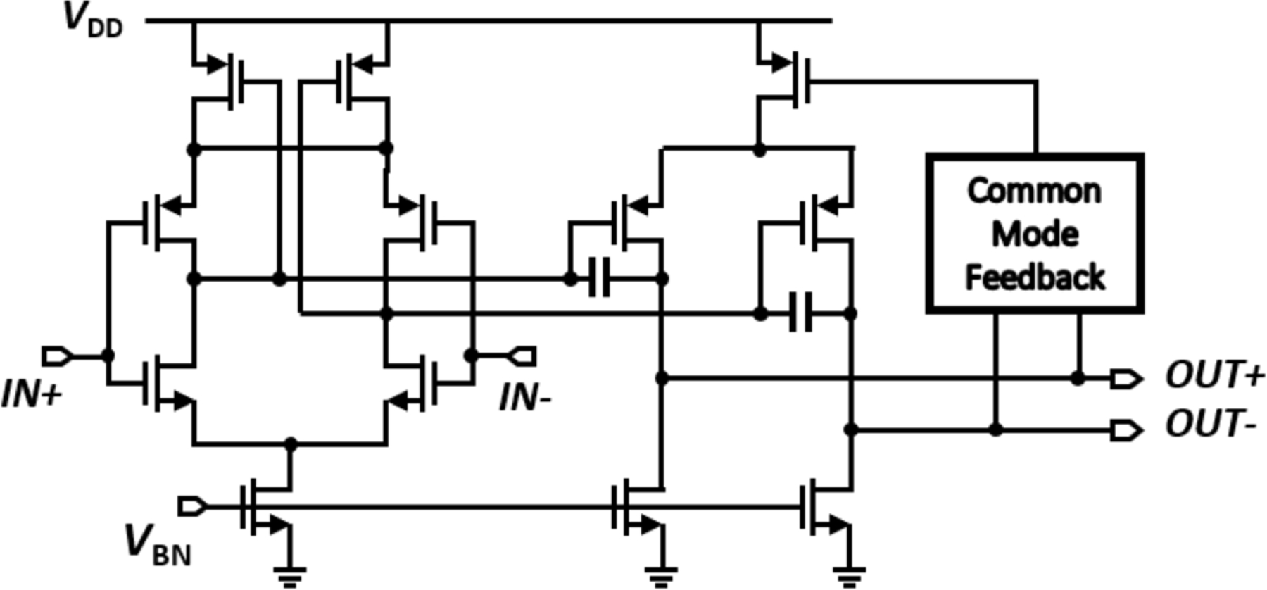
Circuit diagram of a two-stage inverter-type fully differential amplifier for LNA.
C. Frequency Modulator
Each frequency modulator (one per AE channel) comprises a passive up-converting mixer and a current-balancing Gm amplifier. The up-converting mixer operates as a modulator with different per-channel modulation frequencies (fM1 − fM4), where the modulation clocks are generated by an oscillator and a clock divider shared across all channels. The switches of the mixer use transmission gates with bidirectional resistive connections.
The transconductance, gmA, of a conventional Gm amplifier using source degeneration (Fig. 6a), can be written as
| (5) |
where gm1 is the transconductance of input MOS (M1), RF is the feedback resistance used for source degeneration, and rno is a drain-source resistance of a current source. For low power-systems, the transconductance of a conventional Gm amplifier is highly susceptible to PVT variation of the input gm1, where gm1RF does not greatly exceed unity.
Fig. 6.

Gm amplifier small signal model: (a) conventional approach; and (b) negative feedback current-balancing architecture.
An alternative Gm amplifier, implemented in our system, employs negative feedback in the first stage and adds an output gm stage, as illustrated in Fig. 6b. The overall transconductance can be written as
| (6) |
where gm1, RF, and rno are as defined in (5), gmA is the transconductance of a negative feedback gm stage, and gmB is the transconductance of an output gm stage. Since gm1rno is much larger than 1 + gm1RF, we can ignore the (1 + gm1RF)/(gm1rno) term even for low-power systems. Therefore, the transconductance variation is determined by gmA and gmB matching, which is easier to control than absolute gm across PVT variation. Fig. 6c shows the implemented circuit diagram, where an additional gm stage is placed in negative feedback as a current-balancing amplifier [19].
IV. Back End Integrated Circuit (BE-IC)
A. Overview
The summed multi-channel current-mode FDM signal from the AE-ICs is sent over a single wire to the back-end IC (Fig. 2). As illustrated in Fig. 7, the FDM input is first converted from the current domain to the voltage domain using a transimpedance amplifier (TIA). A single-to-differential amplifier (S2D) converts the single-ended voltage to differential voltage for fully differential demodulation circuitry and analog-to-digital conversion (ADC). The demodulation clocks are internally generated by a RC relaxation oscillator and a clock divider, where the oscillator output is also sent via cable to the AE-IC for phase-aligned modulation and demodulation. Individual circuit blocks of the BE-IC are described here in more detail.
Fig. 7.

Block diagram of back-end integrated circuit (BE-IC) for demodulation and digitization of the summed FDM signal from the active electrodes.
B. TIA and Single-to-Differential Conversion
A transimpedance amplifier (TIA), which converts the summed input current to a voltage signal, has a gain determined by the feedback resistor RFB. The TIA bandwidth was designed as 300 kHz to provide multi-channel modulation frequency range for kilohertz-bandwidth ExG signals of interest and higher modulation frequencies (100 kHz and above), though only the lower frequency portion is utilized at present. In this system, we implemented a single-to-differential (S2D) converter with two single-ended amplifiers and three resistors [20]. The transfer function of the S2D circuit can be written as
| (7) |
where Vin is the single-ended input, Voutp and Voutn are the differential outputs, and R1−3 are resistors that define the gain of the S2D amplifier. Since R1−3 are designed to be same value, the gain is two in this system. The reference ground of S2D is externally set to avoid a voltage saturation by an offset error.
A two-stage folded cascode amplifier is implemented and used in both the TIA and S2D circuits. In order to increase drive strength, a class-AB buffer is applied to the amplifier [21]. The TIA does not have an explicit feedback capacitance for stabilization, but this is sufficient for the four-channel implementation. It is likely that scaling the architecture to more FDM channels (or much longer wires) would necessitate explicit capacitance to assure stable operation.
C. Frequency Demodulator
The frequency demodulator for each channel consists of a down-converting mixer and a low-pass filter (LPF). For the down-conversion mixer, the combined, modulated signal from the AEs is demodulated by four different demodulation frequencies (fM1 −fM4) generated by a relaxation oscillator and a clock divider. Since the reference clock from the BE-IC oscillator supports both AE and BE, modulation and demodulation frequencies are effectively synchronous, as the phase delay across the cable is negligible compared to the kilohertz-scale clock frequency. There are four dividers with different division factors (3, 4, 5, 7) in the clock divider, producing four different demodulation clocks in each AE using the reference clock. As the demodulated signal still contains unwanted higher frequency artifacts, a low-pass filter (LPF) follows the down-conversion mixer for filtering. This filter also acts as an anti-aliasing filter for the ADC input.
D. SAR Analog-to-Digital Converter
To digitize the demodulated signal, selected by a 4:1 multiplexer (MUX), an 11-bit successive-approximation register (SAR) analog-to-digital converter (ADC) was implemented in this system. A SAR ADC has been used to provide low-power, moderate resolution data converter. As a small unit capacitance for the SAR capacitor array reduces power consumption, a 7fF standard finger metal-oxide-metal (FMOM) capacitor was used as the unit capacitor in this work, as metal-insulator-metal (MIM) capacitor structures have a larger minimum unit capacitance in this technology. Additionally, as switching within the capacitive digital-to-analog converter (CDAC) is a primary source of power consumption, a merged capacitor switching (MCS) topology was implemented to reduce switching energy [22].
We note that sharing the ADC among channels does introduce time-division multiplexing (TDM) as well to the architecture, and alternatively N ADCs could be implemented. Conventional TDM at the electrode side requires a switch matrix, and it does not provide the mains and motion artifact resilience provided by amplitude modulation; whereas, conventional TDM at the back-end required one signal wire per active electrode. In this design, TDM is used only after demodulation to enable ADC resource sharing.
E. RC Relaxation Oscillator
An offset-compensated RC oscillator, shown in Fig. 8, was implemented for generating the system-wide modulation reference clock in the back-end integrated circuit. The oscillator architecture uses a switch matrix with two-phase operation to attenuate the offset of the comparator and to improve long-term stability of the oscillator for low-power systems [23]. Fig. 8a describes the architecture with the input-referred offset due to mismatch and process variation of the comparator, and Fig. 8b shows the timing diagram for this operation. The clock period, tper, can be written as
| (8) |
where Rext is a variable external resistor, IB1 and IB2 are current sources, C1 and C2 are the capacitors, and VOS is the comparator offset. The effect of this offset, VOS, on tperiod significantly decreases when the components (IB1 and IB2, C1 and C2, respectively) are well matched.
Fig. 8.

Implemented RC oscillator; (a) circuit diagram, (b) timing diagram.
V. Measurement Results and Discussions
A combined prototype of the four-channel, frequencydivision multiplexing active-electrode IC and demodulating back-end IC was implemented in a general purpose 0.18µm silicon CMOS process. A die photo is shown in Fig. 9 with primary functional blocks annotated; total die area is 1mmx3mm. While both front-end AE and back-end circuits were implemented in the same IC area for fabrication, separate dice were used to physically separate the front-end and back-end over a long 3-wire cable (Fig. 2) during all presented experimental testing. The cable provides a clock signal to the from BE to AE, the combined FDM data wire from AE to BE, and a common ground reference shared from BE to AE.
Fig. 9.
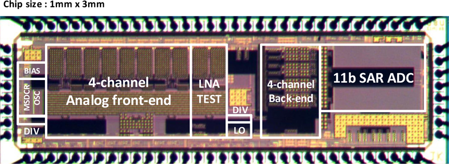
Die photo of the AE-BE IC.
A. Active Electrode LNA Characterization
The measured ac gain response for the active electrode LNA is shown in Fig. 10a. The mid-band amplitude of the LNA is 34dB, where the effective resistance of the proposed MS-DCR is 10X larger than is achievable by conventional duty-cycled resistance. The cutoff frequency can be adjusted by controlling the switching clock duty-cycle. However, the series-connected resistance boosting techniques, including cascaded MS-DCR, introduces a parasitic capacitance at the shared node, which creates an additional pole in the frequency response. For the MS-DCR measurement shown in Fig. 10a, this causes a resulting peaking of the ac gain near the cutoff frequency [24], [25]. This effect can be mitigated using various approaches [26]; one simple modification is to apply a bypass capacitor, which does not increase power consumption, and another approach is to employ an additional Gm amplifier in the negative feedback.
Fig. 10.
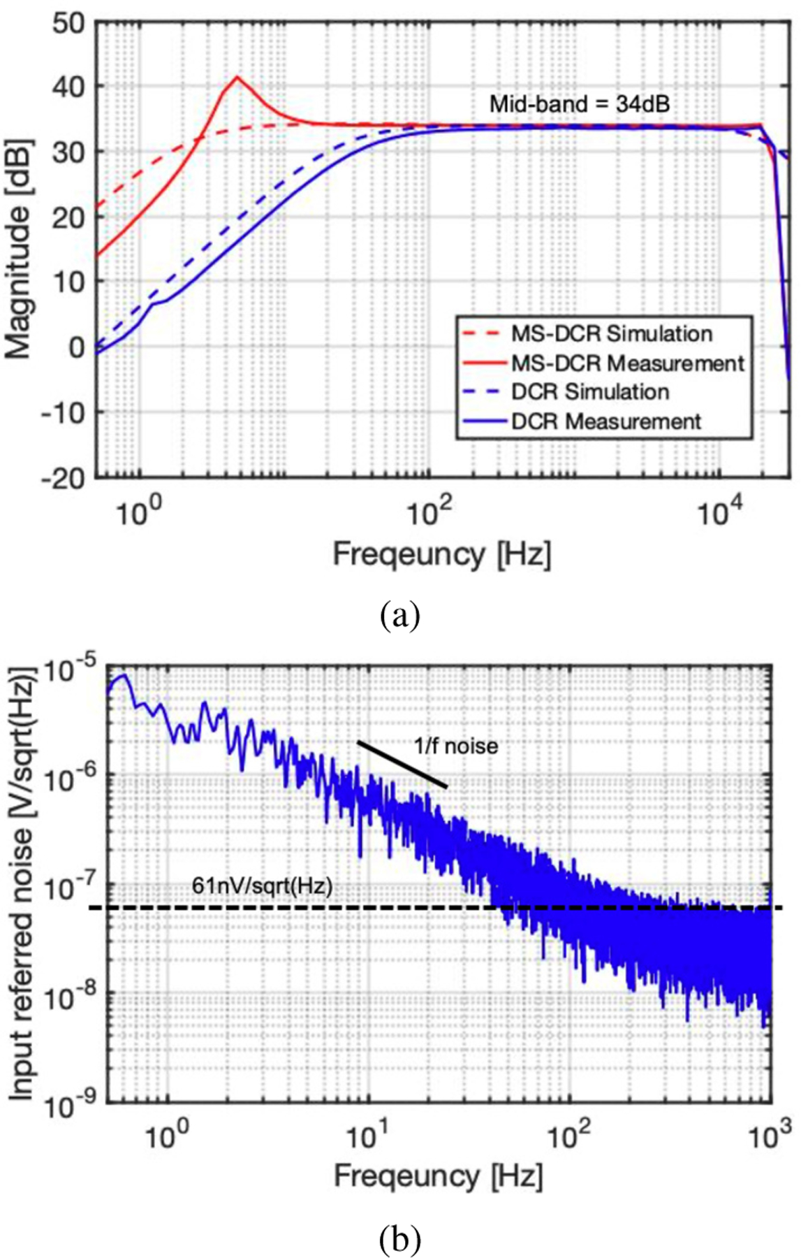
(a) Measured and simulated active-electrode LNA ac response with conventional duty-cycled resistor (DCR) and with the enhanced multi-switching duty-cycled resistor (MS-DCR); and, (b) measured input-referred noise of the active-electrode LNA.
The sharp roll-off at approximately 20 kHz of the measured response compared to the simulated result is due to the inclusion of an on-chip analog buffer at the LNA output using a two-stage amplifier; this was added only for external probing of the node from a pad, and this buffer is not part of the AE signal chain.
As measured, the total input-referred noise of the LNA from 1 Hz to 150 Hz is 3.52 µVrms, where the input-referred thermal noise is as depicted in Fig. 10b.
B. Active Electrode FDM Cross-talk
Cross-talk between channels is present in all FDM-based systems to a greater or lesser degree, where modulation artifacts and harmonic tones are located in the signal band of another frequency channel. For this system, cross-talk was measured between channels, as shown in Fig. 11. Full-scale sinusoidal input voltages were applied to two channels, 1.4 mVrms at 50 Hz and 100 Hz into Channel 1 and Channel 3, respectively; Channel 2 and Channel 4 were both driven with a common-mode dc voltage. Each channel was modulated by a different modulation frequency in the AE, using 1.28 kHz, 1.8 kHz, 2.25 kHz, and 3 kHz for Channels 1–4, where the reference clock is set to 9 kHz. As shown, the demodulated output signals demonstrate 48 dB half-differential (54 dB fully-differential) in-band gain for the 50 Hz and 100 Hz input signals. The measured cross-talk signal magnitude between adjacent channels (CH3 and CH4) is 32 dB lower than the primary signal. As needed, cross-talk can be further reduced by increasing the spacing between the modulation frequencies.
Fig. 11.

Measured crosstalk of the complete four-channel FDM system with two sinusoidal inputs (CH1, CH3) and two dc VCM inputs (CH2, CH4).
C. Mains and Motion Artifact Rejection
Experimental setups for demonstrating the cable noise rejection provided by the implemented FDM-based architecture are illustrated in Fig. 12. In order to mimic motion artifacts, a programmable mechanical shaker was connected to a 3m cable connected between AE and BE. While applying a dc input into the AE IC, we analyzed the noise performance of the FDM-based architecture through a signal analyzer connecting the output of the BE-IC (Fig. 12a).
Fig. 12.

Illustration of the experimental setup for testing rejection of cable noise induced directly in the primary AE-BE cable due to up-conversion using FDM: (a) 20 Hz cable motion artifacts created using a programmable mechanical shaker, and (b) 60 Hz mains interference induced by proximity to powered electrical equipment.
In a similar way, Fig. 12b shows the measurement setup for 60 Hz interference induced by nearby electrical devices injected into the AE-BE cable. In this test environment, the AE-BE cable was looped and placed on the surface of a powered electrical machine to mimic ambient mains noise.
Measured results demonstrating motion artifact and mains interference reduction in the communication cable are depicted in Fig. 13. For measuring a 20 Hz motion artifact, operation of the system using FDM reduces the induced noise by greater than 15X at 20 Hz compared operation of the system without FDM enabled. Also, most of the harmonics induced from main vibration frequency are removed by FDM, as shown in Fig. 13(a). Measured reduction of 60 Hz ambient mains interference injected wirelessly into the AE-BE cable from nearby electrical equipment (Fig. 13(b)) demonstrates that operation of the system with FDM enables improves noise performance greater than 62X compared to operation of the system without FDM enabled.
Fig. 13.

Measured results induced cable noise reduction in the primary AEBE cable due to up-conversion (amplitude modulation), using the experimental setups described in Fig. 12: (a) 15X reduction of 20 Hz cable motion artifacts, and (b) >60X reductions of induced 60 Hz mains interference in the primary cable.
As a further application demonstration of cable noise reduction specific to bioelectrical signal acquisition, a pre-recorded ECG signal taken from the MIT-BIH database [30] was used as an input signal of AM-FDM system using a programmable waveform generator. As shown in Fig. 14, measured results demonstrate mitigation of mechanically-induced 20 Hz cable motion artifacts (Fig. 13(a)) by up-conversion of the signals prior to transmission over the three-wire AE-BE cable bundle.
Fig. 14.

As a further ExG example, measured reduction of induced cable motion artifacts is shown using AM-FDM system for ECG application; experimental setup is similar as in Fig. 12 for inducing 20 Hz cable motion artifacts, and signal input to the AE is a pre-recorded EMG waveform.
D. Four-channel EMG using AM-FDM System
A wearable, FDM-based four-channel EMG readout system prototype has been demonstrated using the implemented AE-IC and BE-IC, as shown in Fig. 15. Commercially available, disposable gel electrodes with Ag/AgCl were used to provide a robust electrical connection [31], [32]. Fig. 15a shows the placement of four surface electrode pairs and one reference electrode for measuring surface biopotential signal changes corresponding to different muscle activations [33]. As shown in Fig. 15b, a battery-powered AE-IC module worn on the arm is connected to a bench-top BE-IC module over a long (3m) three-wire interface. The measured, demodulated transient output signals demonstrate that the AM-FDM system enables distinguishing of wrist extension/flexion and hand closing/opening gestures from the surface EMG measurements (Fig. 15c), providing initial proof-of-concept for the proposed AM-FDM ExG approach.
Fig. 15.
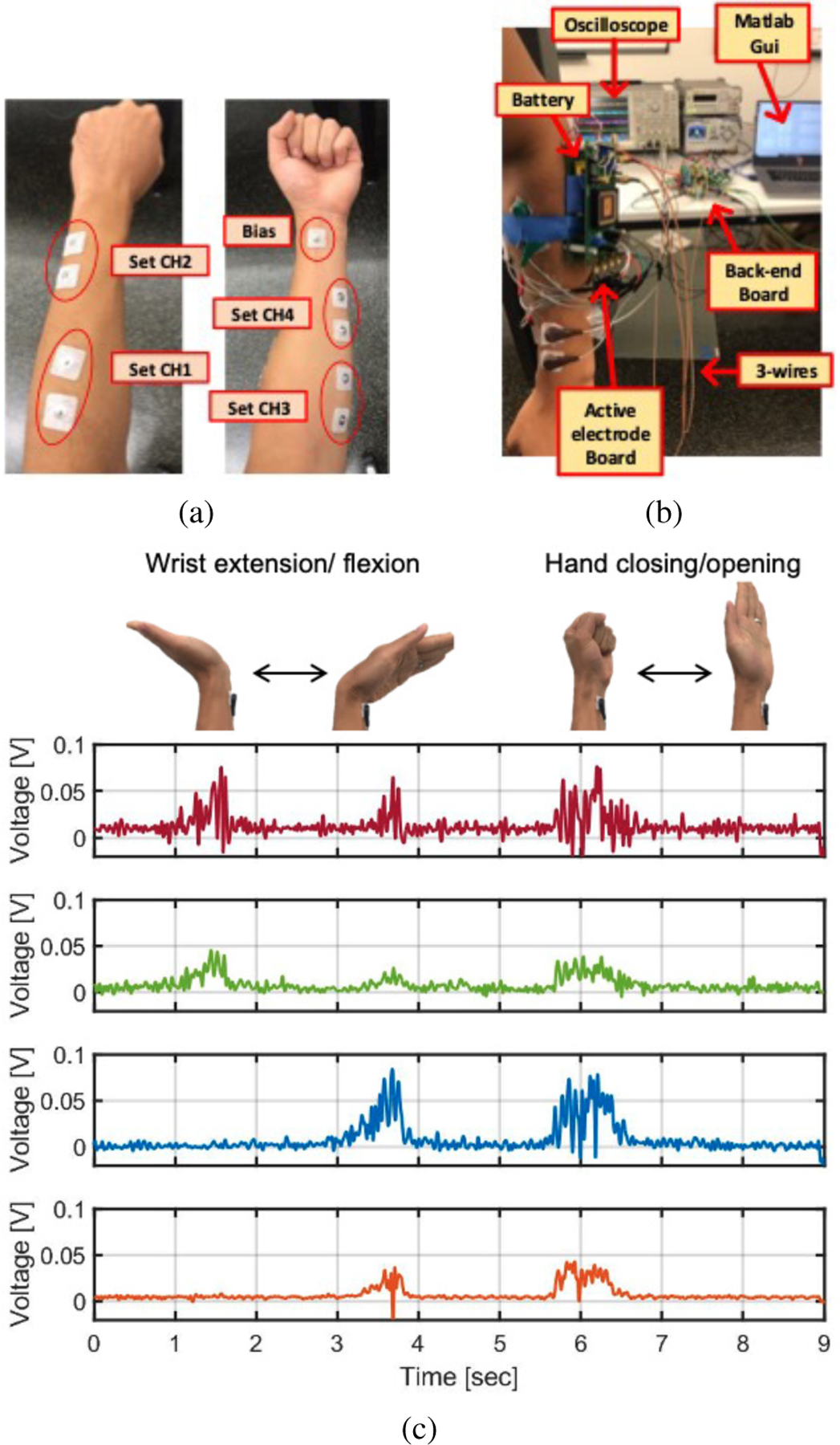
The implemented AM-FDM four channel EMG system demonstration: (a) Electrode position; (b) Experimental setup; (c) Measured results.
E. AM-FDM Power Consumption
A key feature of the implemented readout system is its low power consumption, which makes it suitable for battery-powered active electrode applications. As shown in Fig. 16, the four-channel AE-IC consumes a total average power of 20.8µW, and the BE-IC supporting four channels consumes approximately 76.5µW, most of which is consumed by the four demodulation circuits, as well as analog buffers for monitoring analog signals. Overall, each combined AE-BE channel consumes 43.8µW in operation, including apportioned ADC power.
Fig. 16.

Power breakdown.
VI. Conclusion
This paper has presented an amplitude modulated, frequency-division multiplexing (AM-FDM) biopotential signal acquisition architecture, which reduces the number of wires required for multi-channel recording systems, and further provides inherent reduction in both cable motion artifacts and 50/60 Hz mains noise induced in the cable bundle. Both a front-end active electrode IC and a back-end demodulation IC were implemented and used together for system-level verification.
The performance of the implemented system is compared with other recent, state-of-the-art bioelectrical measurement systems in Table I. The use of passive up-conversion and down-conversion mixers mitigates additional power consumption often required for FDM. In addition, a cascaded multi-switching duty-cycled resistor (MS-DCR) used in the instrumentation amplifier feedback network extends the effective resistance of conventional DCR for high-gain operation.
As shown in Table I, while improving power consumption and removing most off-chip components, overall noise performance is less competitive in the prototype IC compared to other approaches. We believe the additional integration gained in this trade-off will be useful for a variety of applications, such as EMG as shown, but as implemented would not be sufficient for lower noise applications, such as EEG or ECoG.
Overall, the proposed four-channel acquisition system was fabricated in a 0.18µm CMOS process and provides 15X reduction in cable motion artifacts and >62X reduction in cable-induced mains interference, and both one-channel ECG and four-channel real-time EMG systems are demonstrated as proof-of-principle applications.
TABLE I.
Performance comparison with state-of-the-art
| JSSC’14 [11] | TBCAS’20 [27] | JSSC’19 [28] | TBCAS’19 [29] | JSSC’15 [13] | TBCAS’19 [14] | This work | |
|---|---|---|---|---|---|---|---|
| Application | EEG/ETI | EEG | ECG | ETI | EXG | EEG | EMG/ECG |
| Electrode type | Passive | Passive | Passive | Passive | Active | Active | Active |
| Multiplexing type | TDM | TDM | AM-FDM | AM-FDM | Digital bus | FM-FDM | AM-FDM |
| N-channel signal wires | 2N | 2N | 2N | 2N | 2 | 1 | 2 |
| Off-chip component | None | None | 8·LO | None | Capacitor | 2·Inductor | Resistor |
| Electrode offset rejection [mV] | ±250 | ±200 | ±125 | - | ±350 | Rail-to-rail | Rail-to-rail |
| Process [nm] | 180 | 180 | 130 | 130 | 180 | 65 | 180 |
| Supply [V] | 1.8 | 1.0 | 1.0 | 1.0 | 1.8 | 1.2 | 1.8 |
| Bandwidth [Hz] | 0.5–100 | 0.5–100 | 0.5–150 | 15k-125k | 0.5–100 | 0–250 | 1–150 |
| Input Impedance [Ω] | 1.2G(20 Hz) | 560M(50 Hz) | - | - | 100M(50 Hz) | 100M | 160M(50 Hz) |
| Input ref. noise [µV rms ] | 1.75(100 Hz) | 0.63(100 Hz) | 1.44(150 Hz) | - | 0.65(100 Hz) | 0.99(250 Hz) | 3.52(150 Hz) |
| CMRR [dB] | 84 | 89 | 112.5 | - | 102 | - | 76 ∗ |
| AE Gain [dB] | 20–40 | 54/60 | 29.3 | - | 40 | - | 35 |
| ADC | 12b SAR | - | 16b SDM | 16b SDM | 12b SAR | 12b SAR | 11b SAR |
| Area per ch. [mm 2 ] | 21.6 | 0.077(only IA) | 0.525(only IA) | 0.87 | 15.75 | 1 | 0.75 |
| Power per ch. [µW] | 82 | 1.5(only IA) | 7.5(only IA) | 118 | 104.4 | 228 | 43.8 |
LO - Local Oscillator IA - Instrumentation Amplifier
Post simulation result
Contributor Information
Jinyong Kim, School of Electrical Engineering and Computer Science, Oregon State University, Corvallis, OR 97331 USA..
Hyunkyu Ouh, School of Electrical Engineering and Computer Science, Oregon State University, Corvallis, OR 97331 USA. He is now with Apple, Inc., Cupertino, CA USA..
Matthew L. Johnston, School of Electrical Engineering and Computer Science, Oregon State University, Corvallis, OR 97331 USA..
References
- [1].Teng X-F, Zhang Y-T, Poon CC et al. , “Wearable medical systems for p-health,” IEEE reviews in Biomedical engineering, vol. 1, pp. 62–74, 2008. [DOI] [PubMed] [Google Scholar]
- [2].Chi YM, Jung T-P, and Cauwenberghs G, “Dry-contact and non-contact biopotential electrodes: Methodological review,” IEEE reviews in biomedical engineering, vol. 3, pp. 106–119, 2010. [DOI] [PubMed] [Google Scholar]
- [3].Bensmaia SJ and Miller LE, “Restoring sensorimotor function through intracortical interfaces: progress and looming challenges,” Nature Reviews Neuroscience, vol. 15, no. 5, pp. 313–325, 2014. [DOI] [PMC free article] [PubMed] [Google Scholar]
- [4].Edenbrandt L and Pahlm O, “Vectorcardiogram synthesized from a 12-lead ecg: superiority of the inverse dower matrix,” Journal of electrocardiology, vol. 21, no. 4, pp. 361–367, 1988. [DOI] [PubMed] [Google Scholar]
- [5].Daniel KR, Courtney DM, and Kline JA, “Assessment of cardiac stress from massive pulmonary embolism with 12-lead ecg,” Chest, vol. 120, no. 2, pp. 474–481, 2001. [DOI] [PubMed] [Google Scholar]
- [6].Trobec R, “Computer analysis of multichannel ecg,” Computers in biology and medicine, vol. 33, no. 3, pp. 215–226, 2003. [DOI] [PubMed] [Google Scholar]
- [7].Negro F, Muceli S, Castronovo AM et al. , “Multi-channel intramuscular and surface emg decomposition by convolutive blind source separation,” Journal of neural engineering, vol. 13, no. 2, p. 026027, 2016. [DOI] [PubMed] [Google Scholar]
- [8].Lucas M-F, Gaufriau A, Pascual S et al. , “Multi-channel surface emg classification using support vector machines and signal-based wavelet optimization,” Biomedical Signal Processing and Control, vol. 3, no. 2, pp. 169–174, 2008. [Google Scholar]
- [9].Maarsingh E, Van Eykern L, Sprikkelman A et al. , “Respiratory muscle activity measured with a noninvasive emg technique: technical aspects and reproducibility,” Journal of Applied Physiology, vol. 88, no. 6, pp. 1955–1961, 2000. [DOI] [PubMed] [Google Scholar]
- [10].Montavont A, Kaminska A, Soufflet C et al. , “Long-term eeg in children,” Neurophysiologie Clinique/Clinical Neurophysiology, vol. 45, no. 1, pp. 81–85, 2015. [DOI] [PubMed] [Google Scholar]
- [11].Xu J, Mitra S, Matsumoto A et al. , “A wearable 8-channel active-electrode EEG/ETI acquisition system for body area networks,” IEEE Journal of Solid-State Circuits, vol. 49, no. 9, pp. 2005–2016, 2014. [Google Scholar]
- [12].Guermandi M, Cardu R, Scarselli EF et al. , “Active electrode ic for eeg and electrical impedance tomography with continuous monitoring of contact impedance,” IEEE transactions on biomedical circuits and systems, vol. 9, no. 1, pp. 21–33, 2014. [DOI] [PubMed] [Google Scholar]
- [13].Xu J, Busze B, Van Hoof C¨ et al. , “A 15-channel digital active electrode system for multi-parameter biopotential measurement,” IEEE Journal of Solid-State Circuits, vol. 50, no. 9, pp. 2090–2100, 2015. [Google Scholar]
- [14].Warchall J, Theilmann P, Ouyang Y et al. , “Robust biopotential acquisition via a distributed multi-channel FM-ADC,” IEEE Transactions on Biomedical Circuits and Systems, vol. 13, no. 6, pp. 1229–1242, 2019. [DOI] [PubMed] [Google Scholar]
- [15].Harrison RR and Charles C, “A low-power low-noise cmos amplifier for neural recording applications,” IEEE Journal of solid-state circuits, vol. 38, no. 6, pp. 958–965, 2003. [Google Scholar]
- [16].Chandrakumar H and Marković D, “5.5 A 2 µW 40mVpp linear-input-range chopper-stabilized bio-signal amplifier with boosted input impedance of 300MΩ and electrode-offset filtering,” in 2016 IEEE International Solid-State Circuits Conference (ISSCC), 2016, pp. 96–97. [Google Scholar]
- [17].Chandrakumar H and Marković D, “A high dynamic-range neural recording chopper amplifier for simultaneous neural recording and stimulation,” IEEE Journal of Solid-State Circuits, vol. 52, no. 3, pp. 645–656, 2017. [Google Scholar]
- [18].Kim J, Ouh H, and Johnston ML, “A 43.8muw per channel biopotential readout system using frequency division multiplexing with cable motion artifact suppression,” in 2020 IEEE Custom Integrated Circuits Conference (CICC). IEEE, 2020, pp. 1–4. [DOI] [PMC free article] [PubMed] [Google Scholar]
- [19].Yazicioglu RF, Merken P, Puers R et al. , “A 60 µw 60 nv/√hz readout front-end for portable biopotential acquisition systems,” IEEE Journal of Solid-State Circuits, vol. 42, no. 5, pp. 1100–1110, 2007. [Google Scholar]
- [20].Liu X, Zhang M, Xiong T et al. , “A fully integrated wireless compressed sensing neural signal acquisition system for chronic recording and brain machine interface,” IEEE Transactions on biomedical circuits and systems, vol. 10, no. 4, pp. 874–883, 2016. [DOI] [PubMed] [Google Scholar]
- [21].Ouh H and Johnston ML, “Code-division multiplex encoding analog front end for current-mode sensor arrays,” IEEE Solid-State Circuits Letters, vol. 1, no. 5, pp. 118–121, 2018. [Google Scholar]
- [22].Hariprasath V, Guerber J, Lee S-H et al. , “Merged capacitor switching based sar adc with highest switching energy-efficiency,” Electronics letters, vol. 46, no. 9, pp. 620–621, 2010. [Google Scholar]
- [23].Paidimarri A, Griffith D, Wang A et al. , “An RC oscillator with comparator offset cancellation,” IEEE Journal of Solid-State Circuits, vol. 51, no. 8, pp. 1866–1877, 2016. [Google Scholar]
- [24].Ng KA and Xu YP, “A compact, low input capacitance neural recording amplifier,” IEEE Transactions on Biomedical Circuits and Systems, vol. 7, no. 5, pp. 610–620, 2013. [DOI] [PubMed] [Google Scholar]
- [25].Ng KA and Xu YP, “A low-power, high CMRR neural amplifier system employing CMOS inverter-based OTAs with CMFB through supply rails,” IEEE Journal of Solid-State Circuits, vol. 51, no. 3, pp. 724–737, 2016. [Google Scholar]
- [26].Kim J, Ouh H, and Johnston ML, “A sub-hertz bandpass low noise amplifier for biopotential signal acquisition with parasitic pole cancellation,” in 2020 IEEE 63rd International Midwest Symposium on Circuits and Systems (MWSCAS). IEEE, 2020, pp. 13–16. [Google Scholar]
- [27].Tang T, Goh WL, Yao L et al. , “A tdm-based 16-channel afe asic with enhanced system-level cmrr for wearable eeg recording with dry electrodes,” IEEE Transactions on Biomedical Circuits and Systems, vol. 14, no. 3, pp. 516–524, 2020. [DOI] [PubMed] [Google Scholar]
- [28].Zeng L, Liu B, and Heng C-H, “A dual-loop eight-channel ECG recording system with fast settling mode for 12-lead applications,” IEEE Journal of Solid-State Circuits, vol. 54, no. 7, pp. 1895–1906, 2019. [Google Scholar]
- [29].Liu B, Wang G, Li Y et al. , “A 13-channel 1.53-mw 11.28-mm 2 electrical impedance tomography soc based on frequency division multiplexing for lung physiological imaging,” IEEE Transactions on Biomedical Circuits and Systems, vol. 13, no. 5, pp. 938–949, 2019. [DOI] [PubMed] [Google Scholar]
- [30].Moody GB and Mark RG, “The impact of the mit-bih arrhythmia database,” IEEE Engineering in Medicine and Biology Magazine, vol. 20, no. 3, pp. 45–50, 2001. [DOI] [PubMed] [Google Scholar]
- [31].Baba A and Burke M, “Measurement of the electrical properties of ungelled ecg electrodes,” Int. J. Biol. Biomed. Eng, vol. 2, no. 3, pp. 89–97, 2008. [Google Scholar]
- [32].Xu J, Mitra S, Van Hoof C et al. , “Active electrodes for wearable eeg acquisition: Review and electronics design methodology,” IEEE reviews in biomedical engineering, vol. 10, pp. 187–198, 2017. [DOI] [PubMed] [Google Scholar]
- [33].Dawes J, Brian M, Bialek H et al. , “Wireless smartphone control using electromyography and automated gesture recognition,” in 2018 40th Annual International Conference of the IEEE Engineering in Medicine and Biology Society (EMBC). IEEE, 2018, pp. 5390–5393. [DOI] [PubMed] [Google Scholar]