Abstract
Scanning probe microscopies and spectroscopies enable investigation of surfaces and even buried interfaces down to the scale of chemical-bonding interactions, and this capability has been enhanced with the support of computational algorithms for data acquisition and image processing to explore physical, chemical, and biological phenomena. Here, we describe how scanning probe techniques have been enhanced by some of these recent algorithmic improvements. One improvement to the data acquisition algorithm is to advance beyond a simple rastering framework by using spirals at constant angular velocity then switching to constant linear velocity, which limits the piezo creep and hysteresis issues seen in traditional acquisition methods. One can also use image-processing techniques to model the distortions that appear from tip motion effects and to make corrections to these images. Another image-processing algorithm we discuss enables researchers to segment images by domains and subdomains, thereby highlighting reactive and interesting disordered sites at domain boundaries. Lastly, we discuss algorithms used to examine the dipole direction of individual molecules and surface domains, hydrogen bonding interactions, and molecular tilt. The computational algorithms used for scanning probe techniques are still improving rapidly and are incorporating machine learning at the next level of iteration. That said, the algorithms are not yet able to perform live adjustments during data recording that could enhance the microscopy and spectroscopic imaging methods significantly.
Keywords: scanning probe microscopy, scanning tunneling microscopy, data processing, data acquisition
Graphical Abstract
INTRODUCTION
During the past four decades, computers have evolved as everyday instruments in research laboratories. Experimentalists benefit from data digitization that has fundamentally changed the process of data acquisition, analysis, and presentation. Theorists have leveraged the computational power and memory space of modern computers to obtain results from physical models previously unsolvable by pen-and-paper approaches. Nanoscale imaging is one of the fields revolutionized by the use of computers. One example that illustrates the power of the computer-aided processes is super-resolution fluorescence microscopy. Invented and pioneered by Hell,1,2 Betzig,3 Moerner,4,5 (S.) Weiss,6 Xie,7 Zhang,2,8 and others, super-resolution microscopy took advantage of real-time computer fitting of point spread functions of the excitation laser profile to overcome the optical diffraction limit. This technique is now driving innovations throughout biological research,2,9 including exploring protein localization patterns in bacteria,10 unraveling amyloid aggregates structures,11 and direct observation of DNA and RNA dynamics in cells and bacteria.12,13
Similar to super-resolution microscopy, scanning probe microscopy (SPM) also uses point-wise nanoscale data to reconstruct entire images. However, instead of shaping light beyond the diffraction limit, a nano-sized sharp tip is rastered near surfaces—SPM is a surface imaging technique. Depending on the feedback mechanism, different observables can be mapped along with topographical information, such as surface electronic structure, mechanical interactions, and electrochemical reactivity, via scanning tunneling microscopy (STM), atomic force microscopy (AFM), and scanning electrochemical microscopy (SECM), respectively, as well as a host of spectroscopic imaging methods that have been developed and applied.14–22 The introduction of laser excitation into SPM adds another data dimension and enables hyperspectral investigation of charge-transfer phenomena and molecular vibrations at the single-molecule level.23–26
The rich information content and the intrinsic oversampling nature of SPM images serve as ideal platforms for developing computer-aided imaging processing routines. This mini review covers the development, acquisition, and implementation of computer-aided imaging acquisition and processing in nanoscale surface images. Specifically, we focus on recent advances in the improvement of scanning patterns and data segmentation of SPM images. This mini review aims to give a general understanding of the progress of computer-aided image processing of SPM images and to look ahead to fully automated information extraction from multimodal date led by machine learning and artificial intelligence (vide infra).
METHODS
Image Acquisition
All SPM techniques share the same imaging principle of using a sharp tip as the probe for nanoscale surfaces. The first member of the SPM family is STM. A typical STM setup consists of a conductive/semiconducting surface and an atomically sharp metal tip brought within close proximity. When a voltage is applied across this nanoscale probe tip-sample junction, there is a net current of tunneling electrons from one side to the other (once any energy gaps are exceeded by the energy of the tunneling electrons). Moving the tip closer to the surface, the probability of electrons tunneling from one side to the other, and thus the current, increase exponentially. Using a feedback loop that maintains a constant tunneling current, the tip-sample distance is automatically adjusted to compensate for nanoscale changes in the surface electronic density of states. By recording the tip height at every scanned pixel, an STM topographic image can be reconstructed. The most common scan pattern is to raster the tip across the surface in a line-by-line fashion (Figure 1a).27 For the first STM image, analog traces of piezoelectric locations were recorded by a chart recorder. Prior to computers, analog traces of piezoelectric locations were recorded by a chart recorder. A three-dimensional surface model was assembled from the original recorder traces with scissors, plexiglass, nails, and a camera to record the pictures of the glued model at different views (Figure 1b).28,29 Later images have been recorded directly to computer and assembled in software.
Figure 1.
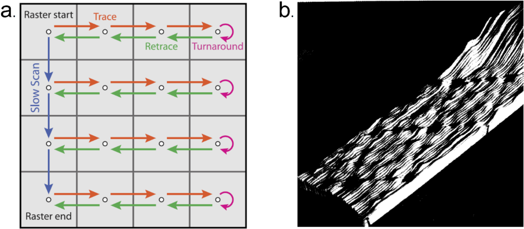
(a) In a linear tip raster pattern, the probe is moved in one direction (orange arrows), is turned around (red arrows) to retrace the line (green arrows), and then advanced to the following line (blue arrows). (b) The first scanning tunneling microscopic observation on the atomic reconfiguration of surface atoms of Si{111}. Image (a) reproduced with permission from ref 27. Copyright 2017 AIP Publishing. Image (b) reproduced with permission from ref 28. Copyright 1987 American Physical Society.
One of the major problems with the scanning pattern from Figure 1a, is the piezoelectric creep and hysteresis that occurs when the velocity of the tip changes by 180° at the end of the trace path (pink arrow in Figure 1a). This sudden change in direction distorts the image and is a time-inefficient method for scanning because the tip needs to return to its original starting position before the next line can be acquired. Some of these issues can be minimized by using a different scanning paradigm or by image processing.
An important contribution to image processing started with mitigating the effects of piezoelectric transducer creep and hysteresis, as STM and AFM both use piezoelectric materials to move the scanning probe tip.30–32 Similarly, Yothers et al. and others have used image post-processing to decompose the components of thermal drift, hysteresis, and creep from their STM images.27,33,34 The processing used a linear transformation correlating the actual tip location with the tip location shown on their images. Matrix elements are used to fit and to minimize the apparent distortions, which enabled recording images to larger scales that are more true to the actual surface. Using an algorithmic approach to image distortions can improve the quality of images acquired through SPM techniques; however, they do not improve the efficiency of image acquisition. In addition, changing the image path algorithm can minimize the effects of hysteresis and creep.
As discussed above, many SPM experiments are performed by rastering a scanning-probe tip across the surface in the fast direction, labeled as trace in Figure 1a, then the tip returns to its original position before it moves one pixel in the slow direction to begin the process again. Though the instrumental design is simple, it also introduces the distortions of creep and hysteresis. Researchers, including Moheimani, have developed a variety of non-rastering patterns to speed up acquisition times.35,36 Ashby and coworkers engineered a version of the spiral raster pattern shown in Figure 2a that is more efficient in time and limits distortion effects.37 By using a mixture of constant linear velocity and constant angular velocity, they have shown an improvement to the simple raster mechanism. To capitalize on the entire image area, they use a constant angular velocity when the tip is close to the center of the image then transition to a constant linear velocity around the edges. Figure 2b is an example of an optimized spiral scanning method with the large image corresponding to the complete scan area. The images to the right correspond to the hashed regions of the total scan area. While varying the scan pattern is not novel,38 Fleming and coworkers found that using non-raster based patterns decreased the time required to image a surface at the expense of an increased vertical bandwith.39 These varied scan patterns also enable researchers to undersample their images decreasing the time required for each subsequent scan.39,40 For other AFM scanning methods, we invite the reader to read the review by Das et al.41
Figure 2.
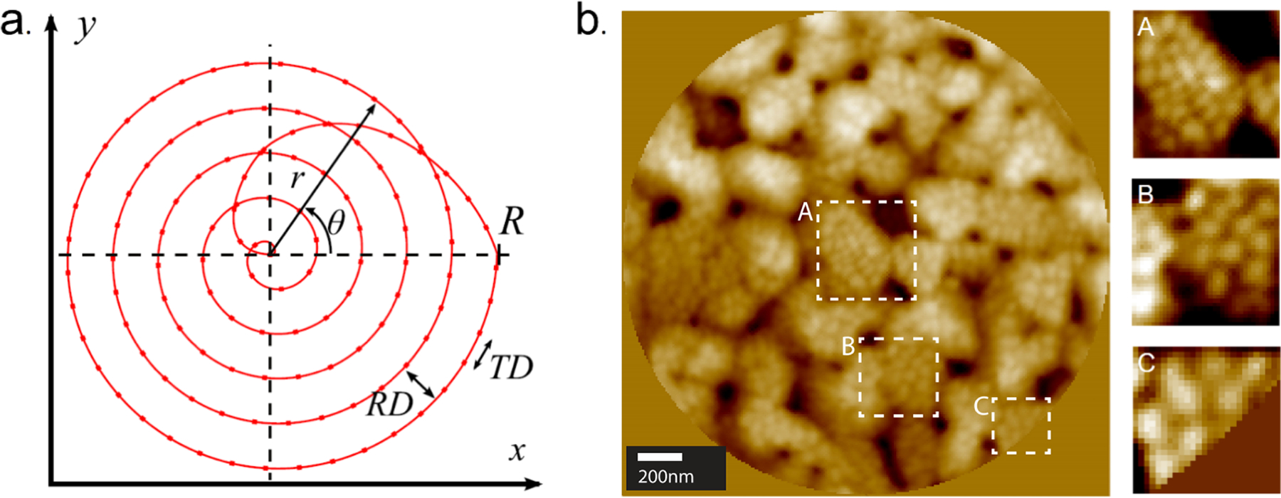
(a) Spiral tip raster pattern implemented for addressing the raster scan paradigm, the probe is moving spirally to minimize the change in acceleration. (b) Optimized spiral-scanning image the three box overlays correspond to the center, middle, and the peripheral imaged regions. Adapted with permission from ref 35. Copyright 2017 IEEE.
Data Segmentation
In addition to improvements to simple image processing and data acquisition, computational methods have also been used for advanced data analysis in STM, particularly in fusing information from different spectroscopic imaging modes. The STM images reveal rich information about the structure of self-assembled monolayers (SAM) since they convey the chemical and physical properties of the studied material. However, the STM images are a convolution of the electronic and geometric information. This convolution makes the images challenging to analyze by a simple computational routine (Figure 3a), such as a planar background subtraction or simple Fourier filters.
Figure 3.
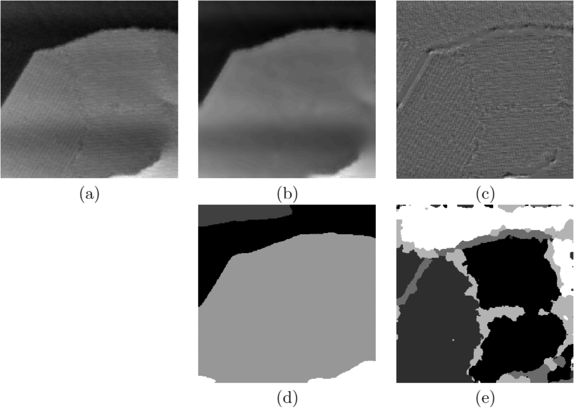
(a) Illustration of the mix of information in a scanning tunneling microscope (STM) image. We observe intensity differences over large regions as well as regions with different textural patterns. These two types of information correspond to specific chemical and physical properties. (b,c) images display the separated cartoon, u, and texture, v, components extracted from the STM image, while images (d,e) show the corresponding segmentation results. Image (a) reproduced with permission from ref 42. Copyright 2016 American Chemical Society. Images (b,c,d,e) reproduced with permission from ref 43. Copyright 2019 Springer Nature.
In Figure 3a, intensity differences occur over large regions in addition to textural (oscillating) patterns. Therefore, the ability to separate regions corresponding to variations of these features (such as significant changes of intensity or textural patterns at different scales and/or orientations) is of the utmost importance in extracting the physical and chemical properties of the observed materials. These properties can include buried functionality and interactions, molecular orientation, tilt angles of individual molecules, molecular conductance, contact conductance, charge redistribution and long-range order of molecular domains.17,44–51
To extract chemical properties,43 STM images can be analyzed using an automated image-processing framework. Since large constant intensity regions and textures carry different information, the first step consists of performing a cartoon (the term cartoon is used since large constant intensity regions look similar to actual cartoon art) and texture decomposition.
The image processing community has widely studied this type of decomposition following the seminal theoretical work of Y. Meyer.52 Most decomposition models consider that the cartoon part (denoted u) and the texture part (denoted v) belong to specific function spaces reflecting their intrinsic characteristics.53–56 Denoting f, the input STM image, these models consist of minimizing some function based on the norms of these spaces, subject to the constraint that f = u+v. A linearized model55 was executed for the simplicity of its numerical implementation as well as its low computational cost (described in detail in ref 57).
Figure 3b and 3c illustrate the cartoon (u) and texture (v) parts extracted from the input image f depicted in Figure 3a, respectively. The next steps are to design segmentation algorithms specialized for each type of component. First, the cartoon part u is segmented using the Local Multiphase Chan-Vese model.58 The Ginzburg-Landeau approximation54 was used to further reduce the expensive computation cost, which can be efficiently computed via the Merriman–Bence–Osher (MBO) scheme.52,60 Figure 3d illustrates the segmentation of the cartoon part given in Figure 3b.
In the image processing community, textures are recognized as the most challenging objects to segment. This challenge is predominantly due to their variability, which avoids the existence of a theoretical model of textures. However, it is widely accepted that textures contain characteristics at different scales and eventually with different orientations. For these reasons, wavelets (and in particular curvelets)59,61 have successfully extracted textures features used to feed some classifiers. Despite these successes, since standard wavelets (or curvelets) correspond to filter banks corresponding to fixed partitioning of the Fourier domain, they are not optimal in capturing the full variability of textures. To remedy this issue, the recently introduced empirical wavelets have been applied for segmentation.62,63
The advantage of empirical wavelets lies in the fact that they are adaptive (i.e., data-driven) wavelets. The wavelets automatically detect the supports, in the Fourier domain, of each wavelet filter leading to the construction of a wavelet decomposition that is “optimal” to extract harmonic (i.e., oscillating) modes. Several types of wavelet, including curvelet, transforms have been revisited and generalized to empirical transforms. Given that both scales and orientations are important textural characteristics in STM images, one can use the energy of the obtained empirical curvelet coefficients to build the expected texture features (note that the superiority of such approaches has been demonstrated for more general texture segmentation/classification tasks in refs 64 and 65).
Finally, feeding the texture features into a multiclass MBO classifier results in the segmentation of the texture component. For example, Figure 3e illustrates the result corresponding to the texture component given in Figure 3c. Note that the algorithm detects the different textures and identifies the boundary regions between textures. In SPM images such boundaries are important clues to structural and other properties.18,66–71
Segmentations obtained from the cartoon and texture parts provide complementary information that is beneficial in understanding the studied material’s physical and chemical properties.47 The complete mathematical description and many more examples showing the efficacy of the proposed framework are available in ref 43. The corresponding Matlab code is freely available at https://github.com/kbui1993/Microscopy-Codes.
For other advanced computational SPM image processing techniques, we direct readers to more thorough reviews by Kalinin and coworkers for detailed discussions of machine learning in analyzing AFM images.70
Using image segmentation, we have been able to differentiate nanoscale surface features in STM images that may be difficult to perceive visually.46 In the field of chemistry, the reactive sites tend to be at the defect sites, including domain boundaries. Specifically, for extracting the chemical information in Figure 3a, we used the aforementioned wavelet algorithm to distinguish regions with similar angular coordinates and frequencies (Figure 4B).42 This image processing method enables grouping regions of the images with similar chemical information, such as the bonding directions of the domains. The regions with different chemical interactions have been given false colors (Figure 4C) to signify the different angular directions of the domains (Figure 4D). Note that multiple domains have similar spacings and orientations. However, viewing these images without these highlights makes grouping of similar domain regions difficult.
Figure 4:
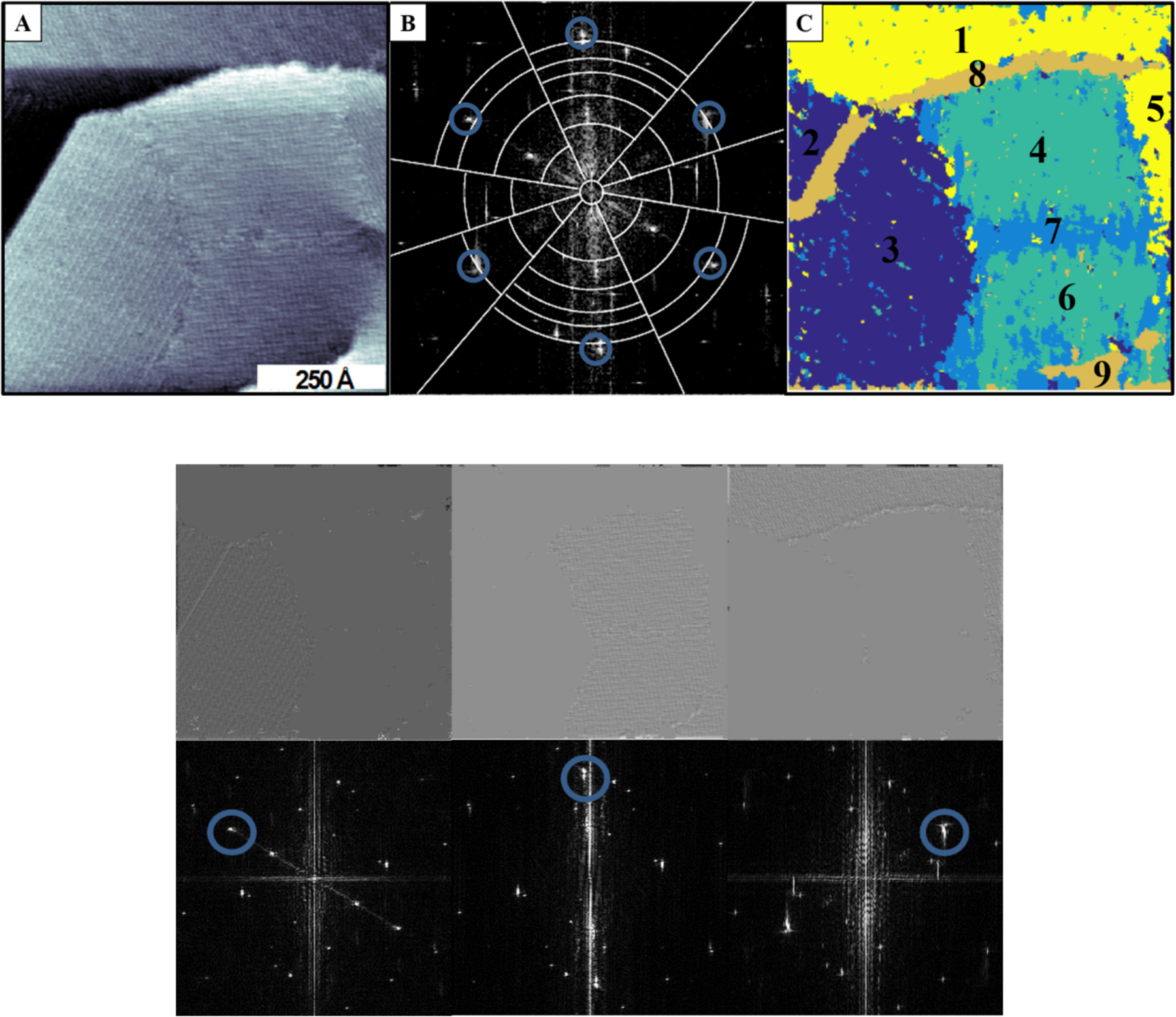
a) Scanning tunneling microscopy image of a thermally annealed sample of AuCN on Au/mica substrate b) Wavelets were used to separate the components of image (a) by angle and frequency. c) False-color reconstruction from wavelet algorithm in (b). Images below show texture relating to the Fourier space below each texture. Reproduced with permission from ref 42 Copyright 2016 American Chemical Society.
We also used empirical wavelets segmentation to separate the textures of the STM image shown in Figure 5A. This process enabled correlating subdomain characteristics of the surfaces to molecular orientations (Figure 5B). Although some subdomain features are easily visible without processing, the interfacial regions can be more challenging to ascertain. Three regions have been assigned where regions 1 and 2 are well-ordered domains with an offset of 120°. Here, classes II, IV, and VI correspond to region 1, and classes I and V correspond to region 2. Finally, class III is composed of the disordered regions that tend to be more reactive than the ordered regions and are likely locations for surface manipulation.
Figure 5:
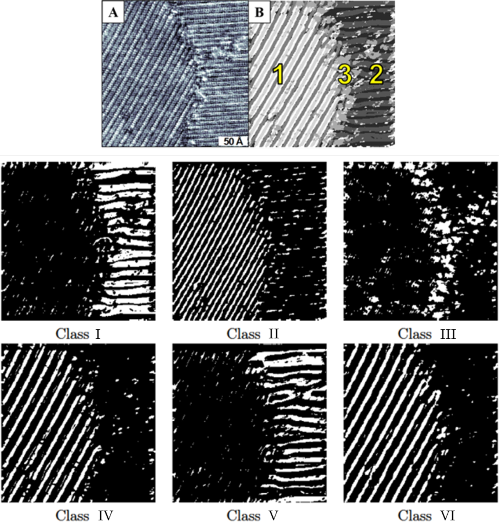
(A) Scanning tunneling microscope image of a self-assembled monolayer of AuCN on a Au/mica substrate (B) Cartoon image of three domains of image (A) composed of six classes (shown above). Adapted with permission from ref 42. Copyright 2016 American Chemical Society.
If complementary experimental measurables can be obtained simultaneously, for example, local barrier height measurments (LBH) and conventional topographic images, chemical information can be extracted by computing the correlations between the two spatially registered data sets. The connections between these two measurements enable resolution of long-range order within SAMs by correlating local maxima of the topography to local maxima of the LBH (Figure 6), which we have shown correspond physically to the exposed and buried ends of the molecules, respectively. Given two hypothetical SPM images containing local maximum data (i.e., p, the blue dots in the topography image and q, the red dots in the LBH image in Figure 6), the corresponding coordinates of p are grouped with q using a block-matching approach. This process is possible because both the topological image and the LBH are acquired simultaneously. The black square and the dashed black square are search windows used for the block-matching process. This procedure is repeated for each p, so p’s and q’s can be linked into a set of vectors that represent the orientations of the individual molecules in the SAM.
Figure 6:
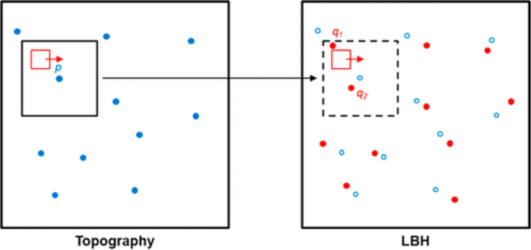
Local maxima in the topography image and local barier height image are defined as p (blue dots) and q (red dots) respectively. The block-matching approach is used to match p and q coordinates. The red square represents the rastering direction. Adapted with permission from ref 46. Copyright 2015 American Chemical Society.
This approach was also used on self-assembled carboranethiol monolayers on Au{111} (Figure 7). Carboranes are composed of carbon–boron cage molecules with each atom bound to one hydrogen; the carboranethiols produce well-ordered monolayers on Au{111} with few defect sites, which by symmetry are limited to translational and rotational offsets in the registry of attachment in complete monolayers.46 However, depending on the locations of the carbons within the caged molecules, there can be a dipole at a variety of angles with respect to the surface normal. Surprisingly, we found that the dipoles within neighboring carboranethiol molecules align within multiple structural domains at low temperature.
Figure 7:
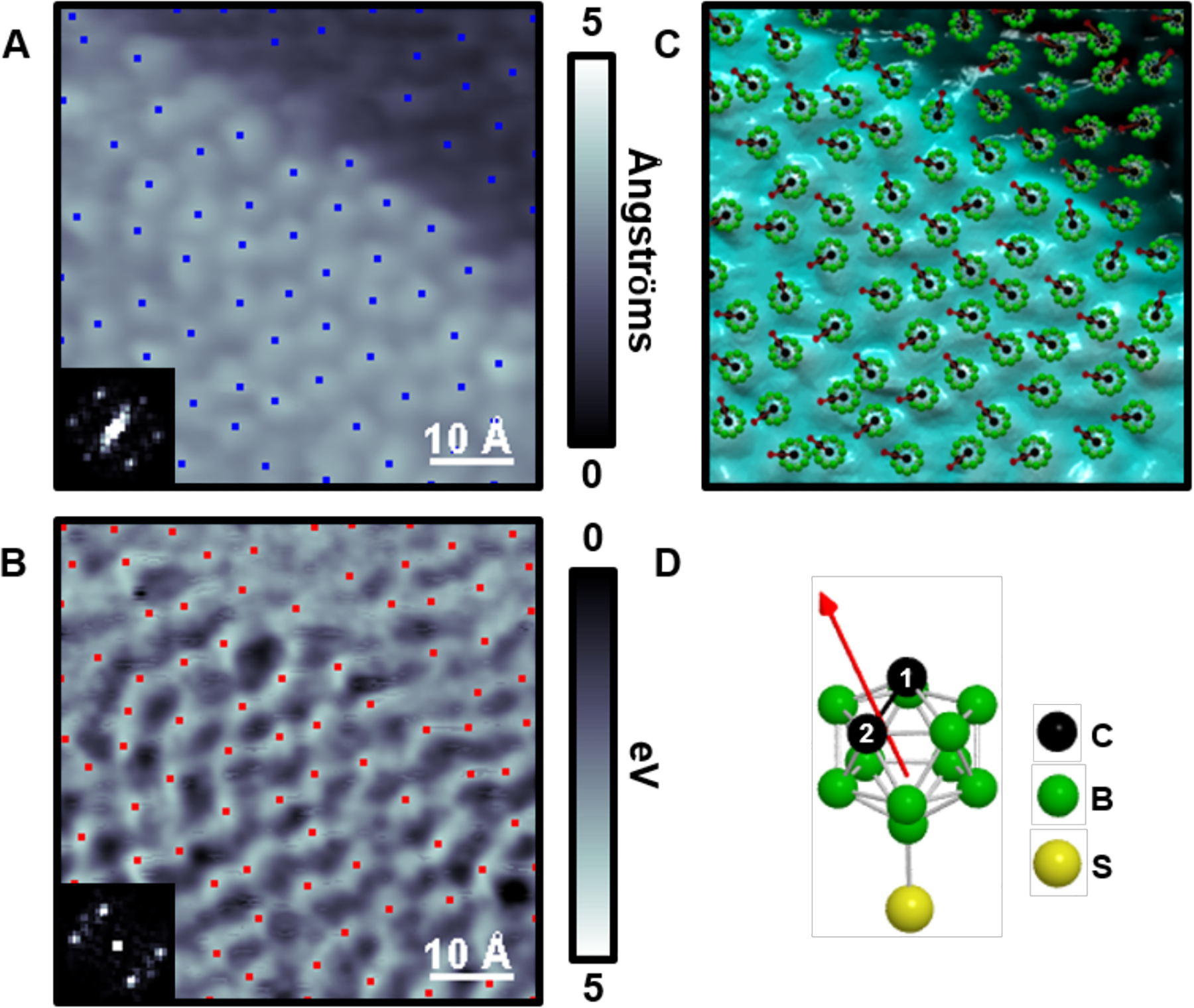
(A) Scanning tunneling micrograph of o-9-carboranethiol (O9) on Au{111} where the blue dots show the local topographic maxima. (B) Simultaneously acquired local barrier height (LBH) image, which is inverted to highlight dipole orientations, with computed local maxima (red). Insets in (A) and (B) depict the fast Fourier transforms (FFTs) of the images. (C) Overlay of the topographic image with the computed molecular dipole orientations. (D) A ball-and-stick model of O9 where hydrogen atoms are omitted for clarity. Adapted with permission from ref 46. Copyright 2015 American Chemical Society.
RESULTS AND DISCUSSION
Hydrogen-Bonding Network and Images
Another use for LBH measurements is to elucidate hydrogen-bonding networks. We studied the long-range hydrogen-bonding networks buried within SAMs using image segmentation.44 Similar to how the dipole directions were measured in Figure 7, the tilts of molecules were measured by correlating the centers of the molecules to the LBH measurements. Using 3-mercapto-N-nonylpropionamide (ATC9), which contains a buried amide group within the monolayer, we found that there were two phases that formed on Au{111} relating to the tilt of the molecules—one with a tilt of 18° while the other was essentially normal to the surface (Figures 8 and 9, respectively). The STM topographic images (Figures 8A and 9A) of both phases were difficult to differentiate; however, the LBH measurements enabled us to assess the relative positions of two parts of the molecule—the top of the molecule and the hydrogen-bonding amide functional group. Schematics of the molecules on the surface are shown in Figures 8C and 9C. It is apparent when the top and bottom of the molecules are not directly overlapping (as can be seen in Figure 8C), the molecular domain has a tilt with respect to the surface normal. Similarly, the local topographic maximums were generally less than 3 Å apart from the LBH maximums within the 0° SAM.
Figure 8:
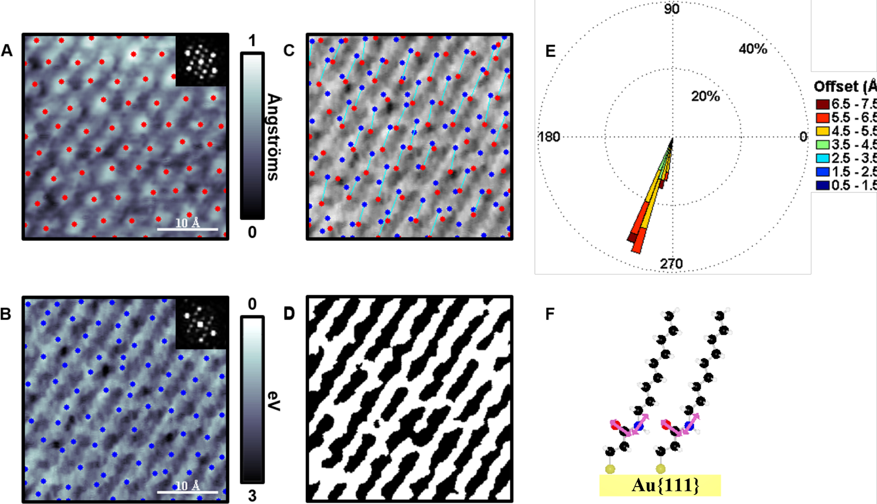
(A) Scanning tunneling microscope topographic and (B) simultaneously acquired local barrier height (LBH) maps over an area of the more tilted (18°) structure of 3-mercapto-N-nonylpropionamide (1ATC9), with respect to the underlying Au{111} surface. The local maxima of both topography (red) and inverted LBH (blue) in B are computed. Insets depict fast Fourier transforms showing the expected topographic hexagonal nearest-neighbor spacing, which is also found within LBH images. (C) All maxima were connected within a defined radial range and orientation; best fit molecular orientations show the expected polar tilt angles. (D) A ball-and-stick model of 1ATC9 showing a polar chain tilt of 18° (for the molecular segment above the amide) and amide bonds nearly parallel to the substrate. Adapted with permission from ref 44. Copyright 2016 American Chemical Society.
Figure 9:
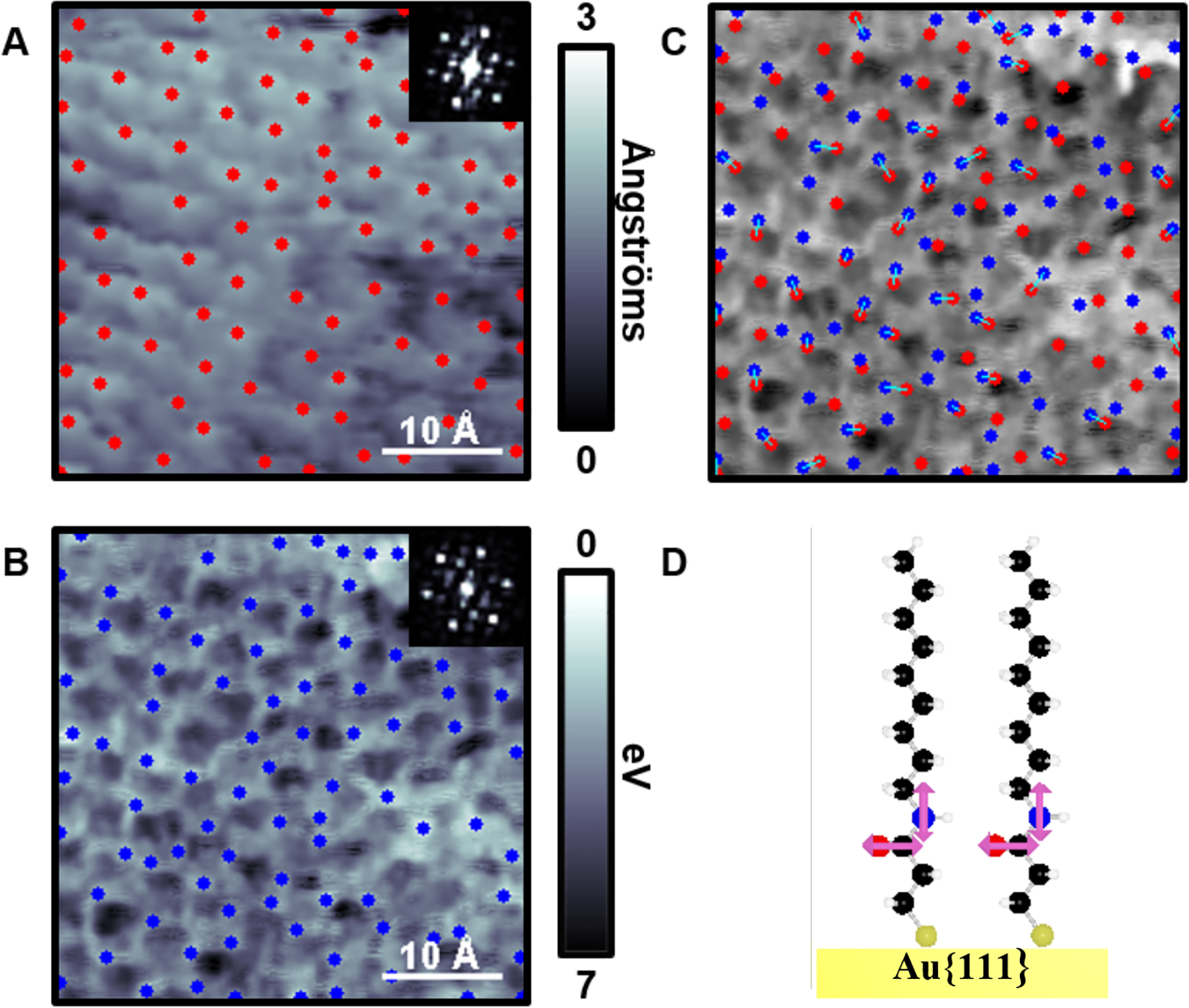
(A) Scanning tunneling microscope topographic and (B) simultaneously acquired local barrier height (LBH) map over the normally oriented (0°) structure, with respect to the underlying Au{111} substrate, within monolayers of 3-mercapto-N-nonylpropionamide (1ATC9). Local maxima in both topography (red) in A and inverted LBH (blue) in B are computed. Insets depict fast Fourier transforms of both topography and LBH images. (C) Computed molecular orientations overlaid onto the LBH map. (D) A ball-and-stick model of 1ATC9 normally oriented on Au substrates. Adapted with permission from ref 44. Copyright 2016 American Chemical Society.
In addition, it is possible to observe both domains within single image frames. Figure 10A and 10B correspond to a region where both domains, 0° and 18°, are in view, where Figure 10A is the topographic measurement and 10B is the LBH measurement. The topographic image appears to have multiple structural domains, however no orientation information can be obtained simply from the image itself. Using the simultaneous acquisition of the LBH measurements, however, the two domains were segmented and stitched together. The blue-shaded region corresponds to the normal phase of the molecules while the red-shaded region corresponds to the 18° tilt phase (Figure 10C). Therefore, to move beyond topography, which contains little chemical information, we can identify the molecular domains and the chemical orientations by correlating the topography with another measurement (in this case LBH). Experimental details and procedures can be found in ref 44.
Figure 10:
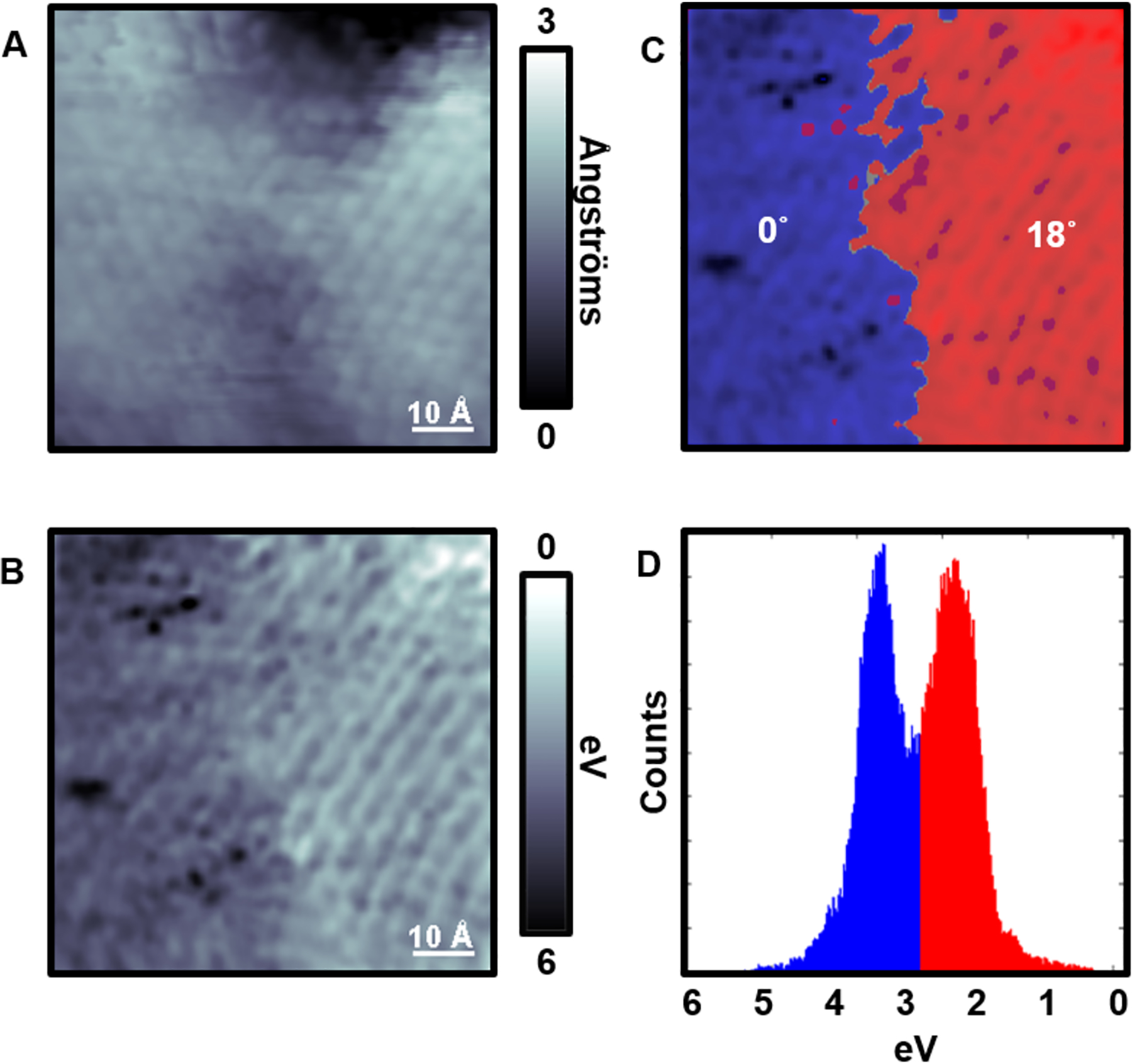
(A) Scanning tunneling micrograph of 3-mercapto-N-nonylpropionamide on Au{111} along a tilt. (B) Simultaneously acquired local barrier height (LBH) image of A. (C) We separate the upper (highlighted as red) and lower (highlighted as blue) domains in LBH based on relative work function differences. (D) Image histogram of C showing the energy cutoff used that was also fit with two Gaussian curves to solve for peak-to-peak image contrast differences. Adapted with permission from ref 44. Copyright 2016 American Chemical Society.
To our surprise, we found that the hydrogen-bonding networks continued across structural domain boundaries and even regions of disorder.44 These observations of robust hydrogen-bonding networks explain the passivating effects of amide-containing alkanethiols, which were observed but not understood at the time of our prior work on the ultrasonic preparation of eutectic gallium-indium (EGaIn) liquid metal nanoparticles.71 In that case, when amide-containing monolayers were uses to protect the liquid EGaIn nanopartices as they were split (calved) to make smaller particles, little oxidation was observed. When n-alkanethiol capping ligands were used, there was significant oxidation of the EGaIn particles.
We have shown two examples in which chemical properties (work function, dipole moment directions, hydrogen-bonding directions, molecular orientations, etc.) were interpreted by using STM and LBH together. These measurements paint a chemical picture more detailed than simply the molecular location that traditional STM measurements yield. In order to understand how molecules are interacting with each other and their substrates, an understanding of the chemical environment is needed.
Functional Materials Properties
Although beyond the scope of the discussion here, we point interested readers to tremendous advances in using analogous machine-learning approaches to explore and to map electrostatic, ferroelectric, liquid crystal orientation, and other properties of functional materials.72–77 Among the pioneers in this area are the Oak Ridge National Lab team, led by Kalinin and co-workers.
CONCLUSIONS AND PROSPECTS
Scanning probe techniques have opened up the atomic-scale world to exploration, including being able to measure bonding and other interactions between molecules and parts of molecules. Increasing power in computational algorithms in the forms of scanning methodologies, fusing complementary information from different imaging modalities, image processing, and image segmentation help elucidate chemical properties at these and larger scales. By correlating the orientations and continuity of interactions, new opportunities beyond chemical bonding distances have been uncovered, which have significant consequences in surface functionalization and passivation, structural biology, and other areas. With this understanding of extended interactions, better materials and assemblies can be designed and fabricated.
Further improvements in these methods will dramatically improve our ability to “see” and to explore the nanoscale world in multiple physical, chemical, and functional dimensions. One key step will be efficiently fusing together multiple acquisition modalities to extract information and understanding. The next generation of SPM techniques will involve more computational algorithms. These opportunities include compressive sensing methods to minimize the number of points acquired without losing information78,79 and by using automated algorithms to manage the processes of sample preparation and image acquisition,80–82 all of which will increase throughput and efficiency in acquiring a “complete” data set in terms of understanding the system under study.
As machine learning improves, gaining efficiency and speed, our ability to use algorithmic platforms will change the way both image collection and image processing are conducted. We target adaptive, real-time, image processing, so as to guide data acquisition to be more information rich and so as to be able to test and to constrain interpretations optimally, as data are being recorded. Though it is improving quickly, the technologies, as of this writing, are not yet able to make strong judgments about images without large libraries of training data. It is more realistic that, in the short term, we will use computational algorithms to increase the efficiency of image acquisition and separate images by quality and features. We will then be able to review images to understand how molecules and assemblies arrange, and with the support from complementary techniques, elucidate the chemistry of the interactions.
Footnotes
The authors declare no competing financial interests.
Contributor Information
Kristopher B. Barr, California NanoSystems Institute and Department of Chemistry and Biochemistry, University of California, Los Angeles, Los Angeles, California 90095, United States.
Naihao Chiang, Department of Chemistry, University of Houston, Houston Texas 77204, United States.
Andrea L. Bertozzi, Department of Mathematics, University of California, Los Angeles, Los Angeles, California 90095, United States.
Jérôme Gilles, Department of Mathematics and Statistics, San Diego State University, San Diego, California 92182, United States.
Stanley J. Osher, Department of Mathematics, University of California, Los Angeles, Los Angeles, California 90095, United States.
Paul S. Weiss, California NanoSystems Institute, Department of Chemistry and Biochemistry, Department of Bioengineering, and Materials Science and Engineering Department, University of California, Los Angeles, Los Angeles, California 90095, United States.
REFERENCES
- (1).Hell SW Nanoscopy with Focused Light (Nobel Lecture). Angew. Chem. Int. Ed 2015, 54, 8054–8066. [DOI] [PubMed] [Google Scholar]
- (2).Hell SW; Sahl SJ; Bates M; Zhuang X; Heintzmann R; Booth MJ; Bewersdorf J; Shtengel G; Hess H; Tinnefeld P; et al. The 2015 Super-Resolution Microscopy Roadmap. J. Phys. D: Appl. Phys 2015, 48, 443001. [Google Scholar]
- (3).Betzig E Single Molecules, Cells, and Super-Resolution Optics (Nobel Lecture). Angew. Chem. Int. Ed 2015, 54, 8034–8053. [DOI] [PubMed] [Google Scholar]
- (4).von Diezmann L; Shechtman Y; Moerner WE Three-Dimensional Localization of Single Molecules for Super-Resolution Imaging and Single-Particle Tracking. Chem. Rev 2017, 117, 7244–7275. [DOI] [PMC free article] [PubMed] [Google Scholar]
- (5).Moerner WE Single-Molecule Spectroscopy, Imaging, and Photocontrol: Foundations for Super-Resolution Microscopy (Nobel Lecture). Angew. Chem. Int. Ed 2015, 54, 8067–8093. [DOI] [PubMed] [Google Scholar]
- (6).Dertinger T; Colyer R; Iyer G; Weiss S; Enderlein J Fast, Background-Free, 3D Super-Resolution Optical Fluctuation Imaging (Sofi). PNAS 2009, 106, 22287–22292. [DOI] [PMC free article] [PubMed] [Google Scholar]
- (7).Zumbusch A; Holtom GR; Xie XS Three-Dimensional Vibrational Imaging by Coherent Anti-Stokes Raman Scattering. Phys. Rev. Lett 1999, 82, 4142–4145. [Google Scholar]
- (8).Huang B; Bates M; Zhuang X Super-Resolution Fluorescence Microscopy. Annu. Rev. Biochem 2009, 78, 993–1016. [DOI] [PMC free article] [PubMed] [Google Scholar]
- (9).Möckl L; Moerner WE Super-Resolution Microscopy with Single Molecules in Biology and Beyond–Essentials, Current Trends, and Future Challenges. J. Am. Chem. Soc 2020, 142, 17828–17844. [DOI] [PMC free article] [PubMed] [Google Scholar]
- (10).Gahlmann A; Moerner WE Exploring Bacterial Cell Biology with Single-Molecule Tracking and Super-Resolution Imaging. Nat. Rev. Microbiol 2014, 12, 9–22. [DOI] [PMC free article] [PubMed] [Google Scholar]
- (11).Sahl SJ; Lau L; Vonk WIM; Weiss LE; Frydman J; Moerner WE Delayed Emergence of Subdiffraction-Sized Mutant Huntingtin Fibrils Following Inclusion Body Formation. Q. Rev. Biophys 2016, 49, e2. [DOI] [PMC free article] [PubMed] [Google Scholar]
- (12).Zhao ZW; Roy R; Gebhardt JCM; Suter DM; Chapman AR; Xie XS Spatial Organization of RNA Polymerase II inside a Mammalian Cell Nucleus Revealed by Reflected Light-Sheet Superresolution Microscopy. Proc. Natl. Acad. Sci. USA 2014, 111, 681–686. [DOI] [PMC free article] [PubMed] [Google Scholar]
- (13).Stracy M; Kapanidis AN Single-Molecule and Super-Resolution Imaging of Transcription in Living Bacteria. Methods 2017, 120, 103–114. [DOI] [PMC free article] [PubMed] [Google Scholar]
- (14).Bonnell DA; Basov DN; Bode M; Diebold U; Kalinin SV; Madhavan V; Novotny L; Salmeron M; Schwarz UD; Weiss PS Imaging Physical Phenomena with Local Probes: From Electrons to Photons. Rev. Mod. Phys 2012, 84, 1343–1381. [Google Scholar]
- (15).Giessibl FJ The qPlus Sensor, a Powerful Core for the Atomic Force Microscope. Rev. Sci. Instrum 2019, 90, 011101. [DOI] [PubMed] [Google Scholar]
- (16).Polcari D; Dauphin-Ducharme P; Mauzeroll J Scanning Electrochemical Microscopy: A Comprehensive Review of Experimental Parameters from 1989 to 2015. Chem. Rev 2016, 116, 13234–13278. [DOI] [PubMed] [Google Scholar]
- (17).Moore AM; Yeganeh S; Yao Y; Claridge SA; Tour JM; Ratner MA; Weiss PS Polarizabilities of Adsorbed and Assembled Molecules: Measuring the Conductance through Buried Contacts. ACS Nano 2010, 4, 7630–7636. [DOI] [PMC free article] [PubMed] [Google Scholar]
- (18).Stranick SJ; Kamna MM; Weiss PS A Low Temperature, Ultrahigh Vacuum, Microwave Frequency – Compatible - Scanning Tunneling Microscope. Rev. Sci. Instrum 1994, 65, 3211–3215. [Google Scholar]
- (19).Feenstra RM; Stroscio JA; Tersoff J; Fein AP Atom-Selective Imaging of the GaAs(110) Surface. Phys. Rev. Lett 1987, 58, 1192–1195. [DOI] [PubMed] [Google Scholar]
- (20).Nienhaus K; Nienhaus GU Where Do We Stand with Super-Resolution Optical Microscopy? J. Mol. Biol 2016, 428, 308–322. [DOI] [PubMed] [Google Scholar]
- (21).Hamers RJ; Köhler UK Determination of the Local Electronic Structure of Atomic - Sized Defects on Si(001) by Tunneling Spectroscopy. Journal of Vacuum Science and Technology A 1989, 7, 2854–2859. [Google Scholar]
- (22).Pitters JL; Wolkow RA Detailed Studies of Molecular Conductance Using Atomic Resolution Scanning Tunneling Microscopy. Nano Lett. 2006, 6, 390–397. [DOI] [PubMed] [Google Scholar]
- (23).Zrimsek AB; Chiang N; Mattei M; Zaleski S; McAnally MO; Chapman CT; Henry A-I; Schatz GC; Van Duyne RP Single-Molecule Chemistry with Surface- and Tip-Enhanced Raman Spectroscopy. Chem. Rev 2017, 117, 7583–7613. [DOI] [PubMed] [Google Scholar]
- (24).Wang S; Chiang N; Guo H; Wattanatorn N; Barr KK; Alexandrova AN; Weiss PS Photoinduced Carrier Generation and Distribution in Solution-Deposited Titanyl Phthalocyanine Monolayers. Chem. Mater 2019, 31, 10109–10116. [Google Scholar]
- (25).Wang S; Wattanatorn N; Chiang N; Zhao Y; Kim M; Ma H; Jen AKY; Weiss PS Photoinduced Charge Transfer in Single-Molecule p–n Junctions. J. Phys. Chem. Lett 2019, 10, 2175–2181. [DOI] [PubMed] [Google Scholar]
- (26).Kradolfer S; Lipiec E; Baldacchini C; Bizzarri AR; Cannistraro S; Zenobi R Vibrational Changes Induced by Electron Transfer in Surface Bound Azurin Metalloprotein Studied by Tip-Enhanced Raman Spectroscopy and Scanning Tunneling Microscopy. ACS Nano 2017, 11, 12824–12831. [DOI] [PubMed] [Google Scholar]
- (27).Yothers MP; Browder AE; Bumm LA Real-Space Post-Processing Correction of Thermal Drift and Piezoelectric Actuator Nonlinearities in Scanning Tunneling Microscope Images. Rev. Sci. Instrum 2017, 88, 013708. [DOI] [PubMed] [Google Scholar]
- (28).Binnig G; Rohrer H; Gerber C; Weibel E 7 × 7 Reconstruction on Si(111) Resolved in Real Space. Phys. Rev. Lett 1983, 50, 120–123. [Google Scholar]
- (29).Binnig G; Rohrer H Scanning Tunneling Microscopy—From Birth to Adolescence (Nobel Lecture). Angew. Chem. Int. Ed. Engl 1987, 26, 606–614. [Google Scholar]
- (30).Croft D; Shedd G; Devasia S Creep, Hysteresis, and Vibration Compensation for Piezoactuators: Atomic Force Microscopy Application, J. Dyn. Sys., Meas., Control 2001, 123, 35–43. [Google Scholar]
- (31).Mokaberi B; Requicha AAG Towards Automatic Nanomanipulation: Drift Compensation in Scanning Probe Microscopes, In IEEE International Conference on Robotics and Automation, 2004. Proceedings of ICRA ‘04, New Orleans, LA, 26 April – 1 May 2004; IEEE: 2004; pp 416–421. [Google Scholar]
- (32).Mokaberi B; Requicha AAG Compensation of Scanner Creep and Hysteresis for AFM Nanomanipulation. IEEE Trans. Autom. Sci. Eng 2008, 5, 197–206. [Google Scholar]
- (33).Ophus C; Ciston J; Nelson CT Correcting Nonlinear Drift Distortion of Scanning Probe and Scanning Transmission Electron Microscopies from Image Pairs with Orthogonal Scan Directions. Ultramicroscopy 2016, 162, 1–9. [DOI] [PubMed] [Google Scholar]
- (34).Horcas I; Fernández R; Gómez-Rodríguez JM; Colchero J; Gómez-Herrero J; Baro AM WSXM: A Software for Scanning Probe Microscopy and a Tool for Nanotechnology. Rev. Sci. Instrum 2007, 78, 013705. [DOI] [PubMed] [Google Scholar]
- (35).Mahmood IA; Moheimani SOR; Bhikkaji B A New Scanning Method for Fast Atomic Force Microscopy. IEEE Trans. Nanotechnol 2011, 10, 203–216. [Google Scholar]
- (36).Yong YK; Bazaei A; Moheimani SOR; Allgöwer F Design and Control of a Novel Non-Raster Scan Pattern for Fast Scanning Probe Microscopy, In 2012 IEEE/ASME International Conference on Advanced Intelligent Mechatronics (AIM), Kaohsiung, Taiwan, 11–14 July 2012; IEEE/ASME: 2012; pp 456–461. [Google Scholar]
- (37).Ziegler D; Meyer TR; Amrein A; Bertozzi AL; Ashby PD Ideal Scan Path for High-Speed Atomic Force Microscopy. IEEE ASME Trans. Mechatron 2017, 22, 381–391. [Google Scholar]
- (38).Yong YK; Bazaei A; Moheimani SOR; Allgöwer F Design and Control of a Novel Non-Raster Scan Pattern for Fast Scanning Probe Microscopy, In 2012 IEEE/ASME International Conference on Advanced Intelligent Mechatronics (AIM), 2012. [Google Scholar]
- (39).Teo YR; Yong Y; Fleming AJ A Comparison of Scanning Methods and the Vertical Control Implications for Scanning Probe Microscopy: Comparison of Scanning Methods Vertical Control Implications for Spm. Asian Journal of Control 2018, 20, 1352–1366. [Google Scholar]
- (40).Niu Y; Han G Fast AFM Imaging Based on Compressive Sensing Using Undersampled Raster Scan. IEEE Trans. Instrum. Meas 2021, 70, 1–9.33776080 [Google Scholar]
- (41).Das SK; Badal FR; Rahman MA; Islam MA; Sarker SK; Paul N Improvement of Alternative Non-Raster Scanning Methods for High Speed Atomic Force Microscopy: A Review. IEEE Access 2019, 7, 115603–115624. [Google Scholar]
- (42).Guttentag AI; Barr KK; Song T-B; Bui KV; Fauman JN; Torres LF; Kes DD; Ciomaga A; Gilles J; Sullivan NF; et al. Hexagons to Ribbons: Flipping Cyanide on Au{111}. J. Am. Chem. Soc 2016, 138, 15580–15586. [DOI] [PubMed] [Google Scholar]
- (43).Bui K; Fauman J; Kes D; Mandiola LT; Ciomaga A; Salazar R; Bertozzi AL; Gilles J; Goronzy DP; Guttentag AI; et al. Segmentation of Scanning Tunneling Microscopy Images Using Variational Methods and Empirical Wavelets. Pattern Anal. Appl 2020, 23, 625–651. [Google Scholar]
- (44).Thomas JC; Goronzy DP; Dragomiretskiy K; Zosso D; Gilles J; Osher SJ; Bertozzi AL; Weiss PS Mapping Buried Hydrogen-Bonding Networks. ACS Nano 2016, 10, 5446–5451. [DOI] [PubMed] [Google Scholar]
- (45).Thomas JC; Goronzy DP; Serino AC; Auluck HS; Irving OR; Jimenez-Izal E; Deirmenjian JM; Macháček J; Sautet P; Alexandrova AN; et al. Acid–Base Control of Valency within Carboranedithiol Self-Assembled Monolayers: Molecules Do the Can-Can. ACS Nano 2018, 12, 2211–2221. [DOI] [PMC free article] [PubMed] [Google Scholar]
- (46).Thomas JC; Schwartz JJ; Hohman JN; Claridge SA; Auluck HS; Serino AC; Spokoyny AM; Tran G; Kelly KF; Mirkin CA; et al. Defect-Tolerant Aligned Dipoles within Two-Dimensional Plastic Lattices. ACS Nano 2015, 9, 4734–4742. [DOI] [PubMed] [Google Scholar]
- (47).Pathem BK; Claridge SA; Zheng YB; Weiss PS Molecular Switches and Motors on Surfaces. Annu. Rev. Phys. Chem 2013, 64, 605–630. [DOI] [PubMed] [Google Scholar]
- (48).Claridge SA; Thomas JC; Silverman MA; Schwartz JJ; Yang Y; Wang C; Weiss PS Differentiating Amino Acid Residues and Side Chain Orientations in Peptides Using Scanning Tunneling Microscopy. J. Am. Chem. Soc 2013, 135, 18528–18535. [DOI] [PMC free article] [PubMed] [Google Scholar]
- (49).Yugay D; Goronzy DP; Kawakami LM; Claridge SA; Song T-B; Yan Z; Xie Y-H; Gilles J; Yang Y; Weiss PS Copper Ion Binding Site in β-Amyloid Peptide. Nano Lett. 2016, 16, 6282–6289. [DOI] [PubMed] [Google Scholar]
- (50).Liu X; Wang L; Li S; Rahn MS; Yakobson BI; Hersam MC Geometric Imaging of Borophene Polymorphs with Functionalized Probes. Nat. Comm 2019, 10, 1642. [DOI] [PMC free article] [PubMed] [Google Scholar]
- (51).Han P; Kurland AR; Giordano AN; Nanayakkara SU; Blake MM; Pochas CM; Weiss PS Heads and Tails: Simultaneous Exposed and Buried Interface Imaging of Monolayers. ACS Nano 2009, 3, 3115–3121. [DOI] [PubMed] [Google Scholar]
- (52).Merriman B; Bence JK; Osher SJ Motion of Multiple Junctions: A Level Set Approach. J. Comput. Phys 1994, 112, 334–363. [Google Scholar]
- (53).Aujol J-F; Chambolle A Dual Norms and Image Decomposition Models. Int. J. Comput. Vision 2005, 63, 85–104. [Google Scholar]
- (54).Aujol J-F; Gilboa G; Chan T; Osher S Structure-Texture Image Decomposition-Modeling, Algorithms and Parameter Selection. Int. J. Comput. Vision 2006, 67, 111–136. [Google Scholar]
- (55).Buades A; Le TM; Morel J-M; Vese L Fast Cartoon + Texture Image Filters. IEEE T. Image Process 2010, 19, 1978–1986. [DOI] [PubMed] [Google Scholar]
- (56).Gilles J Multiscale Texture Separation. Multiscale Model. Sim 2012, 10, 1409–1427. [Google Scholar]
- (57).Buades A; Le T; Morel J-M; Vese L Cartoon + Texture Image Decomposition. Image Processing On Line 2011, 1. [DOI] [PubMed] [Google Scholar]
- (58).Wang X-F; Huang D-S; Xu H An Efficient Local Chan-Vese Model for Image Segmentation. Pattern Recognition 2010, 43, 603–618. [Google Scholar]
- (59).Donoho D; Duncan M Digital Curvelet Transform: Strategy, Implementation and Experiments. Proc. SPIE 2000, 4056, 12–29. [Google Scholar]
- (60).Merriman B; Bence JK; Osher S Diffusion Generated Motion by Mean Curvature, In Proceedings of the Geometry Center Workshop, 1992. [Google Scholar]
- (61).Candès EJ; Demanet L; Donoho DL; Ying L Fast Discrete Curvelet Transforms. Multiscale Modeling and Simulation 2005, 5, 861–899. [Google Scholar]
- (62).Gilles J; Tran G; Osher S 2D Empirical Transforms. Wavelets, Ridgelets and Curvelets Revisited. SIAM J. Imaging Sci 2014, 7, 157–186. [Google Scholar]
- (63).Gilles J Empirical Wavelet Transform. IEEE T. Signal Proces 2013, 61, 3999–4010. [Google Scholar]
- (64).Huang Y; Zhou F; Gilles J Empirical Curvelet Based Fully Convolutional Network for Supervised Texture Image Segmentation. Neurocomputing 2019, 349, 31–43. [Google Scholar]
- (65).Huang Y; Bortoli VD; Zhou F; Gilles J Review of Wavelet-Based Unsupervised Texture Segmentation, Advantage of Adaptive Wavelets. IET Image Process. 2018, 12, 1626–1638. [Google Scholar]
- (66).Poirier GE Characterization of Organosulfur Molecular Monolayers on Au(111) Using Scanning Tunneling Microscopy. Chem. Rev 1997, 97, 1117–1128. [DOI] [PubMed] [Google Scholar]
- (67).Cygan MT; Dunbar TD; Arnold JJ; Bumm LA; Shedlock NF; Burgin TP; Jones L; Allara DL; Tour JM; Weiss PS Insertion, Conductivity, and Structures of Conjugated Organic Oligomers in Self-Assembled Alkanethiol Monolayers on Au{111}. J. Am. Chem. Soc 1998, 120, 2721–2732. [Google Scholar]
- (68).Dziaugys A; Kelley K; Brehm JA; Tao L; Puretzky A; Feng T; O’Hara A; Neumayer S; Chyasnavichyus M; Eliseev EA; et al. Piezoelectric Domain Walls in Van Der Waals Antiferroelectric CuInP2Se6. Nat Commun 2020, 11, 3623. [DOI] [PMC free article] [PubMed] [Google Scholar]
- (69).Claridge SA; Liao W-S; Thomas JC; Zhao Y; Cao HH; Cheunkar S; Serino AC; Andrews AM; Weiss PS From the Bottom Up: Dimensional Control and Characterization in Molecular Monolayers. Chem. Soc. Rev 2013, 42, 2725–2745. [DOI] [PMC free article] [PubMed] [Google Scholar]
- (70).Kalinin SV; Ziatdinov M; Hinkle J; Jesse S; Ghosh A; Kelley KP; Lupini AR; Sumpter BG; Vasudevan RK Automated and Autonomous Experiments in Electron and Scanning Probe Microscopy. ACS Nano 2021, 15, 12604–12627. [DOI] [PubMed] [Google Scholar]
- (71).Hohman JN; Kim M; Wadsworth GA; Bednar HR; Jiang J; LeThai MA; Weiss PS Directing Substrate Morphology via Self-Assembly: Ligand-Mediated Scission of Gallium–Indium Microspheres to the Nanoscale. Nano Lett. 2011, 11, 5104–5110. [DOI] [PubMed] [Google Scholar]
- (72).Balke N; Maksymovych P; Jesse S; Kravchenko II; Li Q; Kalinin SV Exploring Local Electrostatic Effects with Scanning Probe Microscopy: Implications for Piezoresponse Force Microscopy and Triboelectricity. ACS Nano 2014, 8, 10229–10236. [DOI] [PubMed] [Google Scholar]
- (73).Balke N; Maksymovych P; Jesse S; Herklotz A; Tselev A; Eom C-B; Kravchenko II; Yu P; Kalinin SV Differentiating Ferroelectric and Nonferroelectric Electromechanical Effects with Scanning Probe Microscopy. ACS Nano 2015, 9, 6484–6492. [DOI] [PubMed] [Google Scholar]
- (74).Ievlev AV; Kalinin SV Data Encoding Based on the Shape of the Ferroelectric Domains Produced by Using a Scanning Probe Microscope Tip. Nanoscale 2015, 7, 11040–11047. [DOI] [PubMed] [Google Scholar]
- (75).Ievlev AV; Morozovska AN; Shur VY; Kalinin SV Ferroelectric Switching by the Grounded Scanning Probe Microscopy Tip. Phys. Rev. B Condens. Matter 2015, 91, 214109. [Google Scholar]
- (76).Ziatdinov M; Maksov A; Kalinin SV Learning Surface Molecular Structures via Machine Vision. npj Comput. Mater 2017, 3, 1–9. [Google Scholar]
- (77).Kalinin SV; Zhang S; Valleti M; Pyles H; Baker D; De Yoreo JJ; Ziatdinov M Disentangling Rotational Dynamics and Ordering Transitions in a System of Self-Organizing Protein Nanorods via Rotationally Invariant Latent Representations. ACS Nano 2021, 15, 6471–6480. [DOI] [PubMed] [Google Scholar]
- (78).Lerner BE; Flores-Garibay A; Lawrie BJ; Maksymovych P Compressed Sensing for STM Imaging of Defects and Disorder. arXiv:2101.06332 [cond-mat] 2021. [Google Scholar]
- (79).Zengin B; Oppliger J; Liu D; Niggli L; Kurosawa T; Natterer FD Fast Spectroscopic Mapping of Two-Dimensional Quantum Materials. arXiv:2102.00054 [cond-mat] 2021. [Google Scholar]
- (80).Wang S; Zhu J; Blackwell R; Fischer FR Automated Tip Conditioning for Scanning Tunneling Spectroscopy. J. Phys. Chem. A 2021, 125, 1384–1390. [DOI] [PubMed] [Google Scholar]
- (81).Krull A; Hirsch P; Rother C; Schiffrin A; Krull C Artificial-Intelligence-Driven Scanning Probe Microscopy. Commun. Phys 2020, 3, 1–8. [Google Scholar]
- (82).Rashidi M; Croshaw J; Mastel K; Tamura M; Hosseinzadeh H; Wolkow RA Deep Learning-Guided Surface Characterization for Autonomous Hydrogen Lithography. Mach. Learn.: Sci. Technol 2020, 1, 025001. [Google Scholar]


