

Abstract
Focused-ion-beam machining is a powerful process to fabricate complex nanostructures, often through a sacrificial mask that enables milling beyond the resolution limit of the ion beam. However, current understanding of this super-resolution effect is empirical in the spatial domain and nonexistent in the temporal domain. This article reports the primary study of this fundamental tradespace of resolution and throughput. Chromia functions well as a masking material due to its smooth, uniform, and amorphous structure. An efficient method of in-line metrology enables characterization of ion-beam focus by scanning electron microscopy. Fabrication and characterization of complex test structures through chromia and into silica probe the response of the bilayer to a focused beam of gallium cations, demonstrating super-resolution factors of up to 6 ± 2 and improvements to volume throughput of at least factors of 42 ± 2, with uncertainties denoting 95% coverage intervals. Tractable theory models the essential aspects of the super-resolution effect for various nanostructures. Application of the new tradespace increases the volume throughput of machining Fresnel lenses by a factor of 75, enabling the introduction of projection standards for optical microscopy. These results enable paradigm shifts of sacrificial masking from empirical to engineering design and from prototyping to manufacturing.
Keywords: chromium oxide, focused ion beam, sacrificial masking, super-resolution
1. Introduction
Nanoscale milling with a focused ion beam enables the direct formation[1] of nanostructures with complex surfaces in three dimensions. This process is broadly applicable to the fabrication of electronic,[2] mechanical,[3] photonic,[4] and fluidic[5] devices, and is becoming increasingly important to prepare samples for materials characterization[6] and biological imaging.[7] Despite the widespread use of the focused ion beam as a machine tool, its limits of resolution and throughput remain unclear, masking its ultimate utility.
Understanding the limits of focused-ion-beam machining begins with focus. A narrow focus of an ion beam with a low current enables patterning of fine features, whereas a high current enables rapid milling of deep features across wide areas. Although the de Broglie wavelength of gallium cations in a conventional focused-ion-beam system is at the femtometer scale, aberrations intrinsic to electrostatic lenses and space-charge effects from Coulomb interactions broaden the focus of such an ion beam into an approximately Gaussian profile at the nanometer scale.[8] For dielectric substrates, exposure to an ion beam results in electrostatic charging and repulsion of ions from the surface, further complicating the process of focusing the ion beam and degrading lateral and vertical resolution. The lateral extent of the ion-beam profile generally follows a power-law dependence on ion-beam current, with effective lateral resolution requiring characterization[9] for specific ion sources and substrate materials. Accordingly, reducing the lateral extent of the focused ion beam, simply by decreasing the current, generally improves lateral resolution and decreases the accumulation of charge. However, a lower current also results in a longer time to mill through the vertical range, prolonging any drift of the system and wear of the aperture that limits current. These issues can degrade lateral resolution[10] to an intolerable extent, while operating costs can accrue to an unsustainable level. Depending on the materials and dimensions, a single workpiece can take tens of hours to machine.
This inherent coupling of lateral resolution and volume throughput yields a tradespace of spatial and temporal constraints. Although an explicit description of this tradespace is absent from the literature, there is a general tendency to consider the focused ion beam as being slow, costly, and more useful for prototyping than for manufacturing, with excursions into the latter domain often relying on pattern replication.[5d,11] In contrast, previous studies have described a tradespace for lithographic processes, finding a power-law relation between lateral resolution and areal throughput[12] extending into the commercial domain of manufacturing.[13] These studies explicitly excluded the focused ion beam from analysis, for several reasons. First and foremost, direct milling conventionally involves a volume throughput rather than an areal throughput, without a separate process of pattern transfer. Second, focused beams of metal ions implant remnants of the machine tool in the workpiece, requiring the additional study of the milling process and material responses. Third, conventional processes at the state of the art of focused-ion-beam machining are commercially viable for only a few products of high value, such as editing circuits[14] and repairing photomasks.[15]
Constraints on lateral resolution motivate the use of sacrificial films[4d,5b,16] to dissipate charge from insulating substrates,[17] protect workpieces from redeposition and damage along the edges of device features,[5b,16b] enable super-resolution of such edges down to the scale of one to ten nanometers,[5b] and prepare samples for microscopy[6,7] and tomography.[10b] In each of these applications, a sacrificial film functions as a physical barrier that masks the workpiece from the diffuse periphery, or tail, of the focused ion beam. This masking process effectively reduces the radius of the ion beam near boundaries of the milling pattern and yields edge profiles that are narrower than and differ in shape from those resulting from direct milling. In this way, sacrificial masking manifests as a super-resolution effect, in which a multiplicative factor quantifies the reduction of edge width and corresponding improvement from a conventional resolution to an unconventional resolution. Despite its common use, current understanding of spatial masking is incomplete, beginning with material selection. Milling rates of polymeric masks[16b,c] exceed those of common substrates such as silica,[18] resulting in soft masks with low values of physical selectivity, a fundamental property of the mask-substrate bilayer. Metallic masks,[4d,5b,16a,d] such as aluminum, platinum, and chromium, have lower milling rates but tend to be polycrystalline, with grain sizes ranging from tens to hundreds of nanometers. Additionally, milling rates depend on grain orientation,[19] transferring surface and line-edge roughness into the substrate,[16d] degrading lateral and vertical resolution, and potentially limiting the accuracy of models of ion transport[20] to understand the bilayer response.
Reductions of electrostatic charging and edge defects are obvious advantages of a conductive sacrificial mask, and the super-resolution effect implies some advantage. However, it is nonobvious that a sacrificial mask presents any fundamental advantage to super-resolve nanostructure edges, in comparison to simply reducing ion-beam current to improve lateral resolution. To answer this open question, which is central to our study, we unmask the resolution–throughput tradespace of focused-ion-beam machining, discovering that a sacrificial mask enables patterning with the effective resolution of a low value of ion-beam current and the volume throughput of a high value of ion-beam current. This dramatic improvement demonstrates that the dominant advantage of the super-resolution effect occurs in the temporal domain, rather than in the spatial domain.
To substantiate this surprising finding, we perform the first comprehensive and systematic study of this topic, integrating five new concepts for the most widely available type of electron-ion beam system at the state of the art (Figure 1). First, we introduce a chromia, Cr2O3, film for electron microscopy and sacrificial masking of silica, characterizing the advantageous properties of this multifunctional masking material (Figure 1a). Second, we demonstrate a new method for in-line metrology of effective lateral resolution, enabling new efficiency and reproducibility (Figure 1b). Third, we pattern complex nanostructures through chromia and into silica, measuring and simulating responses of the bilayer to ion exposure, and quantifying vertical resolution and lateral super-resolution (Figure 1c). Fourth, we develop a model of the super-resolution effect, achieving good agreement with experimental data, simulating the super-resolution of conventional test structures, and elucidating the temporal efficiency of the process (Figure 1d). Fifth, we test our model predictions in an application of sacrificial masking to the fabrication of arrays of Fresnel lenses, increasing volume throughput by a factor of 75 relative to a single, functionally equivalent lens that we fabricate directly into silica with a low value of ion-beam current (Figure 1e). These results demonstrate paradigm shifts of focused-ion-beam machining through sacrificial masks, from empirical to engineering design of processes for device fabrication and sample preparation, and from prototyping single devices to manufacturing device arrays and otherwise surpassing the volume throughput limit of conventional resolution.
Figure 1.
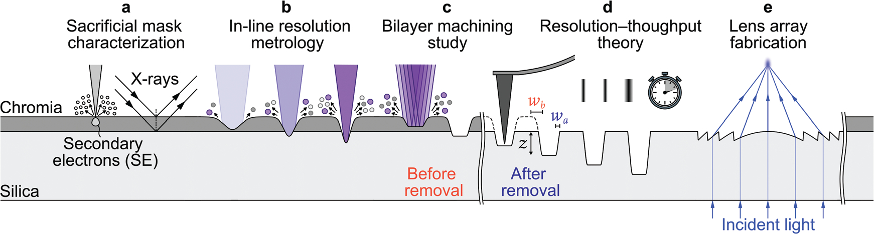
Experimental overview. a) Materials characterization reveals the structure and solid state of a sacrificial mask of chromia on a silica substrate. b) In-line resolution metrology enables reproducible and optimal focus of a beam of gallium cations. c) Study of the bilayer structure before and after removal of the chromia elucidates milling responses. d) Theory predicts spatial and temporal advantages of masking the periphery of the ion beam with a sacrificial film. e) Application of the resolution–throughput tradespace increases volume throughput of the fabrication of Fresnel lens arrays.
2. Results and Discussion
2.1. Materials Characterization
The semiconducting behavior,[21] nanometer roughness,[22] gigapascal hardness,[22b,23] and high selectivity in chemical etching of chromia against silica make this material a good candidate for our application. We form a silica film by thermal oxidation of a silicon substrate, over which we form a chromia masking film by sputter deposition[24] (Note S1, Supporting Information). To comprehensively characterize our bilayer and provide input quantities for theoretical models, we combine atomic force microscopy, scanning electron microscopy, transmission electron microscopy, and X-ray diffraction (Note S2, Supporting Information).
2.1.1. Surface Structure
The silica surface has a subnanometer root-mean-square roughness and sparse asperities with a height of 1.6 ± 0.2 nm (Figure S1, Supporting Information). We report all uncertainties as 95% coverage intervals, or we note otherwise. Atomic force micrographs provide estimates of the lower bound[25] of root-mean-square roughness of 0.3 ± 0.2 nm for silica and 0.6 ± 0.2 nm for chromia (Figure 2a). X-ray diffractometry data are generally consistent with these measurements, yielding estimates of root-mean-square roughness of 0.4 ± 0.4 nm and 1.5 ± 0.4 nm (Figure 2g and Table S1, Supporting Information). Scanning electron micrographs of the chromia surface indicate negligible charging during imaging and show lateral roughness ranging in scale from 10 to 40 nm (Figure 2b). We report quantitative ranges of experimental data as 95% coverage intervals. Discrete Fourier transforms of atomic force micrographs (Figure 2d) and of scanning electron micrographs (Figure 2e) indicate an aperiodic structure of the chromia surface.
Figure 2.
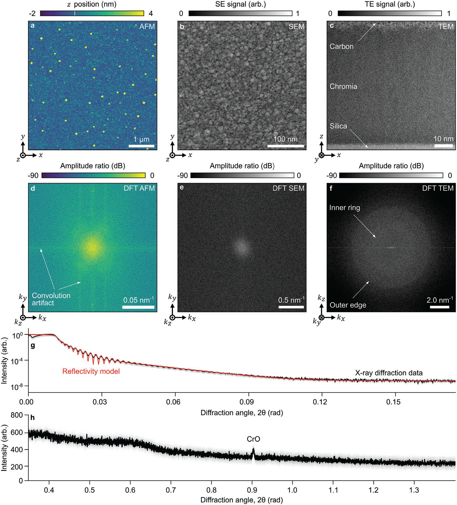
Chromia characterization. a) Atomic force micrograph and b) scanning electron micrograph showing the surface structure of the chromia mask on silica before milling with a focused ion beam. c) Transmission electron micrograph showing a cross section of the chromia mask. The carbon is an artifact of sample preparation. d–f) Plots showing discrete Fourier transform (DFT) of the micrographs in (a–c). The origin, corresponding to a spatial frequency of 0 nm−1, occurs at the center of each image. Horizontal and vertical lines in (d) indicate the presence of a convolution artifact of the probe tip in atomic force micrographs. g) Plot showing (black) a grazing-incidence 2θ scan of X-ray diffraction and (red) a fit of an X-ray reflectivity model[26] with a reduced chi-square statistic, , of 0.4. h) Plot showing a conventional 2θ scan of X-ray diffraction. The gray regions around the black lines in (g,h) indicate intensity distribution widths as 95% coverage intervals.
2.1.2. Volume Structure
Ellipsometry data show a silica thickness of 488 ± 2 nm. Consistent with our measurements of surface roughness by X-ray diffraction, transmission electron micrographs show a chromia thickness of 63 ± 2 nm (Figure 2c and Table S1, Supporting Information). In discrete Fourier transforms of these transmission electron micrographs (Figure 2f), a diffuse inner region with a sharp outer edge around 4.0 nm−1 indicates a generally amorphous composition, which is consistent with X-ray diffraction data. A fit of a reflectivity model[26] to the X-ray diffraction data yields a chromia thickness of 65 ± 3 nm and density of 5.3 ± 0.1 g cm−3 (Figure 2g). The X-ray diffraction pattern of the chromia (Figure 2h) shows a broad peak of low intensity below angles of 0.7 rad (40°), indicating that the chromia is generally amorphous, and a narrow peak of low intensity at 0.901 ± 0.003 rad (51.6° ± 0.2°), suggesting the presence of crystalline domains of CrO[27] with a size of approximately 40 nm.
2.2. In-Line Resolution Metrology
Having comprehensively characterized our bilayer, we load a sample into an electron–ion beam system and focus both beams. Scanning electron microscopy offers the potential to measure and optimize the effect of the focused ion beam prior to nanofabrication. In such a process, the system operator mills an open cavity or pit, the simplest test structure, by dwelling the focused ion beam in a single position for a certain amount of time. Measurement of the radius of the pit by scanning electron microscopy quantifies the effective lateral resolution of the focused ion beam. Manual focusing of the ion beam proceeds by iteratively adjusting the voltage of the final lens in the ion-beam column, milling a new pit, and measuring its radius. This process can occur in real time if a fast method for dimensional metrology is available, and concludes with the estimation of a minimum radius, indicating that the focus of the ion beam is near optimal.
There are two main challenges of such in-line measurements. The first is physical, as scanning electron microscopy is sensitive to dielectric charging, which our chromia mask mitigates. The second is analytical, as scanning electron microscopy yields an indirect measure of surface topography, with image contrast resulting primarily from local tilt, shadow, and material contrast.[28] Previous studies have taken different approaches to analyze the resulting images, yielding different combinations of efficiency and accuracy. Simple approximations without uncertainty evaluation[9] are unsuitable for dimensional metrology, whereas accurate physical models[29] of scanning electron microscopy require energy-loss functions of the constituent materials. Historically, these functions have required synchrotron measurements to obtain. Intermediate approaches can achieve both efficiency and accuracy, such as by using reference data from a physical model to calibrate an empirical model.[30]
2.2.1. Image Formation
We introduce an efficient method of measuring pit radius by scanning electron microscopy, in comparison to independent measurements of surface topography by atomic force microscopy (Figure 3a,b and Table S2, Supporting Information). We make the novel observation of a near equality of pit radii corresponding to the maximum signals of secondary electrons in scanning electron micrographs (Figure 3d), and the maximum convexity of surface profiles in atomic force micrographs, where the negative value of the second derivative of the surface profile with respect to position is maximal (Figure 3e). This empirical correlation implies that the curvature of our test pits affects image formation, which we interpret by topographic calculations of tilt and shadow contrast (Note S3 and Figure S2, Supporting Information). This new analysis suggests that the implantation of gallium, sputtering and redeposition of chromia and silica, and resulting material contrast near the region of maximum convexity contributes to signal peaks in scanning electron micrographs. Further study is necessary to fully understand the cause of this empirical correlation, which we nonetheless put to good use.
Figure 3.
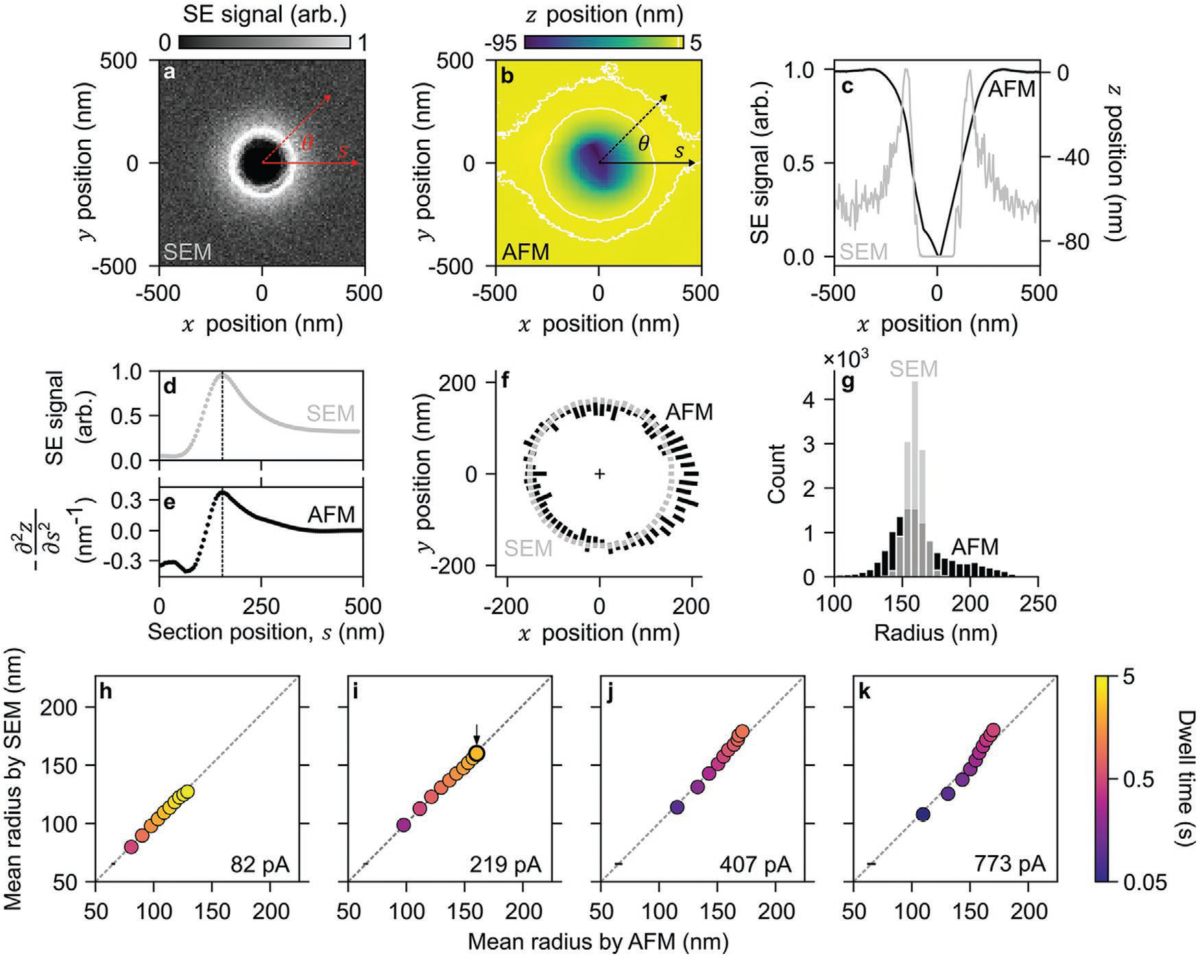
In-line resolution metrology. a) Scanning electron micrograph and b) atomic force micrograph showing a representative pit in the chromia-silica bilayer. c) Plots showing (gray) secondary electron signals from (a) and (black) z position from (b) for horizontal line scans through the center of either image. d) Plot showing the secondary electron scattering intensity along a radial section from (a) in the direction of the largest radius of the pit. e) Plot showing the negative of the second derivative of the z position of the pit along a radial section from (b) in the direction of the largest radius of the pit. f) Plots showing angular dependence of pit radius for all values of section angle from (gray) scanning electron microscopy (SEM) and (black) atomic force microscopy (AFM) after smoothing. Bars indicate radius distribution widths as 95% coverage intervals. g) Histograms showing pit radius for all values of section angle of ten replicates from (gray) scanning electron microscopy and (black) atomic force microscopy. h–k) Plots showing correlative measurements of mean radius of pits by atomic force microscopy and scanning electron microscopy for one decade of ion-beam current and two decades of dwell time. (a–g) Correspond to the black circle and arrow in (i). The lone black bars near the lower left corner of the plots in (h–k) indicate representative uncertainties of mean radius as 95% coverage intervals. More details are in Tables S2 and S3 and Notes S3 and S4, and Figures S3 and S4, and Table S4 (Supporting Information).
2.2.2. Correlative Measurements
For a representative test pit, we compare a section from a scanning electron micrograph (Figure 3c) to a section of the negative of the second derivative from an atomic force micrograph (Figure 3d). The micrographs show pit asymmetry due to several non-ideal conditions of milling and microscopy, including astigmatism and drift of the focused ion beam during patterning and an artifact from probe-sample convolution in atomic force micrographs (Note S4 and Figures S3 and S4, Supporting Information). As a result, scanning electron microscopy yields a relatively narrow and approximately normal distribution of pit radius, whereas atomic force microscopy yields a relatively broad and asymmetric distribution of pit radius (Figure 3e). Regardless, the two measurements of mean pit radius agree to within a root-mean-square error ranging from 4 to 7 nm (Figure 3f–j and Table S4, Supporting Information). These values are comparable to our estimate of statistical uncertainty for atomic force microscopy and range from 3% to 5% of the pit radii. Even better, our estimate of statistical uncertainty for scanning electron microscopy has a 95% coverage interval of 1 nm, whereas accurate measurements with physical models can achieve a total uncertainty of approximately 1 nm, including systematic effects.[29] These results show that our new approach to in-line metrology of effective lateral resolution is usefully precise, although further study is necessary to quantify systematic effects that limit accuracy. These results build confidence in our method of minimizing the radii of test pits, which we use to focus our ion-beam prior to nanofabrication of complex test structures.
2.3. Complex Test Structures
2.3.1. Ion Exposure
In contrast to lithographic patterning, which requires pattern transfer and is generally serial for each vertical feature dimension, focused-ion-beam milling directly forms complex nanostructures. To quantify the relationships between milling depth, mask thickness, effective lateral resolution, and volume throughput, we mill checkerboard patterns through the chromia mask and into the underlying silica (Figure 4a,b and Figure S5, Supporting Information). The depths vary from 0 to 200 nm before removal of the chromia and from 0 to 130 nm after removal of the chromia by selective chemical etching. This complex pattern tests lateral resolution at the edges of square structures, which are more robust than pit or line structures to artifacts from probe-sample convolution in atomic force micrographs (Note S5, Supporting Information). Subsequent simulations of conventional line-space arrays supplement our experimental test structures.
Figure 4.
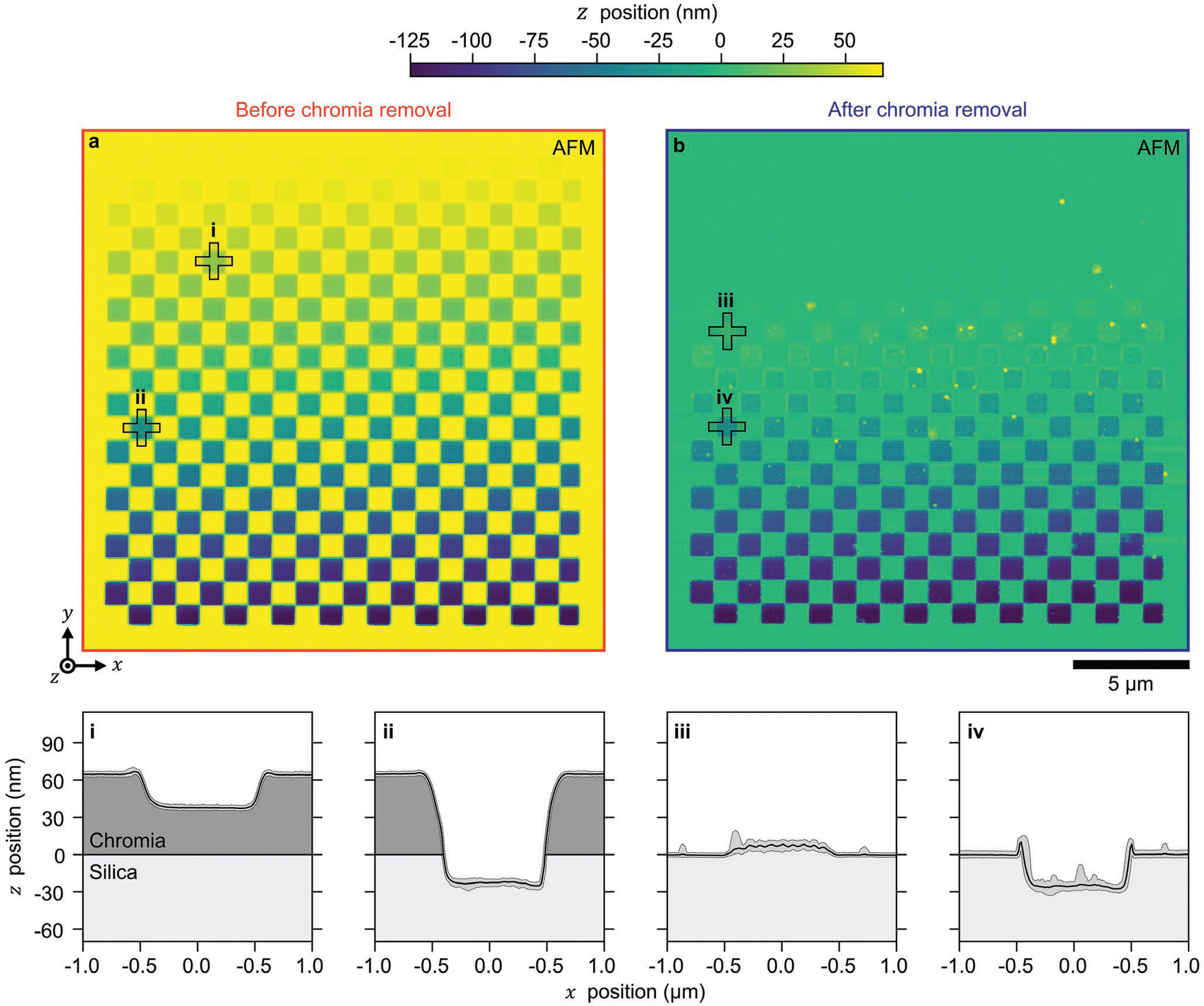
Complex test structures. a,b) Atomic force micrographs showing representative checkerboard patterns a) before and b) after removal of the chromia mask. i–iv) (Black profiles) Sections from atomic force micrographs showing representative features before and after removal of the chromia mask. The gray shading around the black profiles indicates distribution widths of sections of atomic force micrographs as 95% coverage intervals. ii,iv) Sections showing the same feature before and after removal of the chromia mask by selective chemical etching, respectively. We define the zero plane to be top of the silica surface. The periodic surface topography within some squares may be due to an aliasing artifact.[5a]
2.3.2. Vertical Responses
Vertical responses of the bilayer include variable milling rates and apparent modification of the material interface. Milling rates increase monotonically through chromia into silica (Figure 5a; Figure S6 and Table S5, Supporting Information). A piecewise-linear approximation of the milling response fits four apparent milling rates. The initial milling rate of chromia is low, which is relevant to patterning near the top surface. At higher doses, the milling rate of chromia triples to a value representative of milling bulk chromia. Milling through bulk chromia, gallium ions penetrate the chromia-silica interface, and the milling rate increases by approximately one third. Milling through the interfacial layer, bulk silica shows a milling rate that again increases by one third, indicating that any initial response of silica, such as a lower milling rate,[5a] occurs through and under the chromia. The ratio of the bulk milling rate of silica to that of chromia exceeds unity, resulting in a physical selectivity of 1.63 +0.61/−0.44 (Table S6, Supporting Information). This fractional notation denotes 95% coverage intervals that are asymmetric. In addition to the critical parameter of physical selectivity, which exceeds unity for this bilayer, crystalline grains and surface roughness of hard masks should be minimal to reduce lateral and vertical anisotropy of the milling process. Our chromia mask performs well in this regard, being predominantly amorphous and having surface roughness of less than 2 nm in comparison to the roughness of the underlying silica surface, which is less than 1 nm (Figure 2a–c).
Figure 5.
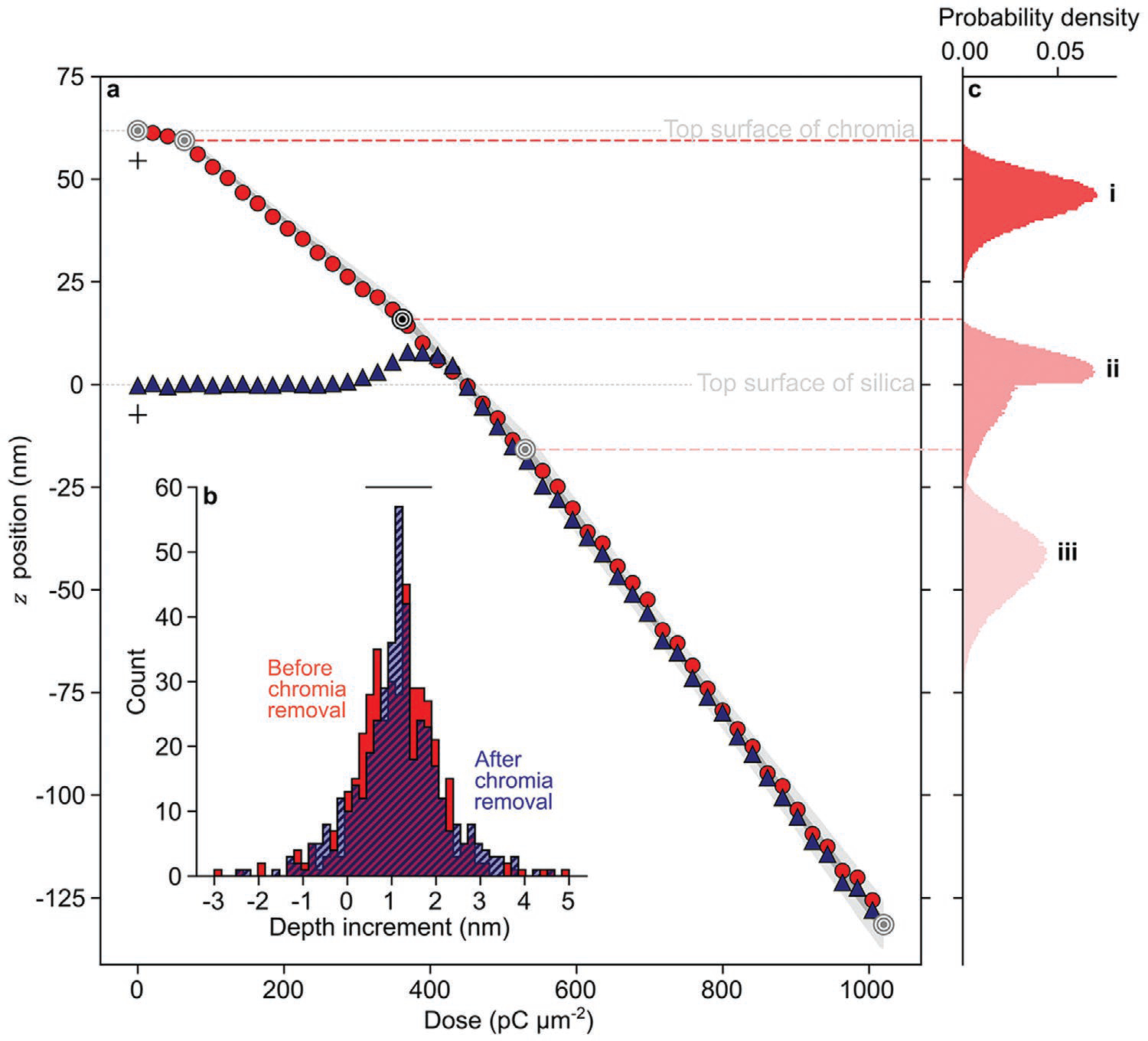
Vertical responses. a) Plot showing milling responses of chromia on silica for an ion-beam current of 227 ± 1 pA (red circles) before and (blue triangles) after chromia removal. Uncertainties of ion-beam currents are conservative estimates of 100% coverage intervals. The light and dark gray regions respectively indicate the 95% coverage interval and the interval between the lower and upper quartiles of the piecewise-linear model of milling responses. The lone black crosses indicate distribution widths of dose and depth respectively as 100% and 95% coverage intervals. b) Histograms showing depth increments (red) before and (blue hatch) after removal of the chromia mask for all ion-beam currents. The lone black bar indicates a representative uncertainty of z position as a 95% coverage interval. c) Histograms showing simulations of stopping range as a function of z position for depths that correspond to (roundels) inflection points in the milling rates of chromia on silica, i) (69 pC μm−2, 59 nm), ii) (366 pC μm−2, 16 nm), and iii) (531 pC μm−2, −16 nm). The lone black roundel indicates the onset of a change in milling rate due to the underlying chromia-silica interface. More details are in Figure S6 and Tables S5–S7 (Supporting Information).
At intermediate doses, nanostructures rise above the zero plane of the chromia-silica interface after exposure to chromium etchant (Figure 4b–iii). In a previous study of a similar substrate, thermal oxide did not swell significantly at low doses,[5a] suggesting that gallium cation penetration modifies the chromia-silica interface, potentially forming a silicate with lower susceptibility to chromium etchant than chromia. Higher doses mill these nanostructures back down through the zero plane (Figure 5a). We achieve our target depth increment of 1 nm in silica, with standard deviations that are within 1 nm of the surface roughness of the silica, down to a depth of 130 nm (Figure 5b and Figure S6, Supporting Information). Depth increment distributions broaden slightly after chromia removal (Table S5, Supporting Information).
To better understand these material responses, we perform three simulations of gallium cation penetration through chromia and silica, elucidating a primary interaction of the machine tool and workpiece. The suitability of amorphous materials for calculation of stopping ranges of ions in matter, and the input parameters from our materials characterization, build confidence in the simulation results. Three histograms of stopping range as a function of depth correspond to bulk chromia, the chromia-silica interface, and bulk silica (Figure 5c-i–iii). The mean stopping range of gallium cations in bulk chromia agrees to within 2 nm with the z position onset of a higher milling rate of the chromia-silica interface (Figure 5c-i–iii and Table S7, Supporting Information). This consistency supports our experimental measurements, piecewise-linear approximations of vertical responses, and simulations of ion penetration.
2.3.3. Edge Profiles
Completing our characterization of the test structures, we quantify widths of nanostructure edges before, wb, and after, wa, removal of the sacrificial mask. Edge and line widths are both straightforward to measure and are both proportional to the radius of the ion beam, which ultimately limits lateral resolution. Accordingly, we use edge width as a metric of effective lateral resolution and super-resolution. Focused-ion-beam milling of the bilayer yields edge profiles that are approximately sigmoidal. Removal of the sacrificial mask changes the shape of the profile, abruptly truncating the sigmoid, which can be advantageous for nanofluidic channels,[5a,b] waveguides,[16a] or for the process of replica molding.[11] Accordingly, the reduction of data from profiles in atomic force micrographs to quantities of edge width requires two different models. To extract widths and depths, we fit an error function to edge profiles before removal of the sacrificial mask, and we truncate an error function to fit to edge profiles after removal (Figure S7, Supporting Information).[31] These approximations originate from integration of a Gaussian function, which is appealing for nanostructure edges resulting from exposure to a focused beam with a profile that is approximately Gaussian. However, edge profiles do include systematic effects from the dependence of milling rate on incidence angle, discontinuities in milling rate within the bilayer, and an apparent overshoot artifact from atomic force microscopy. Even so, a novel Monte-Carlo statistical analysis with jack-knife resampling shows that measurement uncertainty dominates our estimates of uncertainty for wb, wa, and resulting super-resolution factors, Figures S7a, S8, and S9 and Tables S8–S10, Supporting Information). After chromia removal, edge widths decrease by factors ranging from 2 for deep features to 6 for shallow features. Shallow features in chromia exhibit wider edges than features of similar depth in silica after removal of the chromia (Figure S8 and Table S8, Supporting Information), indicating that the sacrificial mask improves lateral resolution for features of similar depth. These results affirm the use of error functions to accurately extract edge widths, building confidence in the reliability of these measurement results and the validity of our subsequent use of error functions in models of spatial masking.
2.4. Resolution–Throughput Tradespace
2.4.1. Theoretical Basis
Characterization of the bilayer response enables a new study of the tradespace of lateral resolution and volume throughput. The effective lateral resolution, , can be either a conventional resolution, , or an unconventional super-resolution, (Note S9, Supporting Information). Effective lateral resolution improves as ion-beam current decreases,[32] but reductions in ion-beam current, I, incur a nonlinear cost of milling time, degrading volume throughput and potentially lateral resolution by drift of the system. To elucidate how sacrificial masks affect this tradespace, we express effective lateral resolution and super-resolution in terms of ion-beam current and equate them. Conventional lateral resolution results from milling a feature of a certain depth directly into a substrate with a low value of ion-beam current, Ilow, whereas super-resolution results from milling a similar feature through a sacrificial mask and into an underlying substrate with a high value of ion-beam current, Ihigh. The super-resolution factor, , relates the two quantities,
| (1) |
where we apply the approximation of a power-law relation of the radius of a focused ion beam with coefficient, α, and exponent, β, the latter of which typically ranges from 0.25 to 1.00 for liquid-metal ion sources with ion-beam currents of less than 10 nA.[32]
To test Equation (1) and further characterize our effective lateral resolution, we fit a power-law model to pit radius (Figure 3h–k) as a function of total charge, and to edge width before and after removal of the chromia mask as a function of ion-beam current (Figure S10, Supporting Information). The trends for the different test structures are generally consistent and yield reasonable values of model parameters (Table S11, Supporting Information), corroborating our results from in-line resolution metrology and building confidence in Equation (1) as the basis of the resolution–throughput tradespace.
An important issue to consider is that Equation (1) presents a theoretical perspective in which ion-beam current is a continuous variable. However, in typical focused-ion-beam systems, apertures limit the selection of ion-beam current to discrete values. Nonetheless, this theoretical perspective yields important insights into the spatiotemporal domain, while also accommodating experimental validation in the spatial domain. To this end, Equation (1) permits a substitution of terms, in which the widths of nanostructures resulting from milling with a single value of ion-beam current, before and after removal of the chromia mask, take the place of the power-law expressions for the radii of ion beams with low and high values of current. The resulting proportionality in Equation (2) avoids the experimental limitation of discrete values of ion-beam current, enabling validation of the kernel of our model of super-resolution with measurements of edge widths before and after removal of the chromia mask,
| (2) |
On the basis of Equations (1 and 2), we introduce new theory, in three aspects, to elucidate the super-resolution effect. First, a model of spatial masking maps patterns of ion dose to resulting nanostructures in chromia and silica to calculate factors of lateral super-resolution, predicting our experimental results without adjustable parameters and fitting other experimental results with adjustable parameters. Second, a model of temporal efficiency uses Equation (1) to account for the different durations of milling a structure of a certain volume by a low or high current, elucidating the temporal advantage of the super-resolution effect. Third, a comparison of the spatial and temporal effects of the sacrificial mask shows dramatic improvements depending on the mask selectivity and thickness, and a figure of merit quantifies performance within the tradespace to guide future optimization.
2.4.2. Super-Resolution
The common approximation of the current density distribution of a focused ion beam by a Gaussian or bi-Gaussian function enables derivation of a closed-form solution to in terms of the complementary error function and geometric and physical parameters of the bilayer. We use the Gaussian approximation for simplicity, and we establish the validity of either approximation in our model of lateral super-resolution (Note S6 and Figure S11, Supporting Information). Our model relates the ratio of edge widths, wb, and wa, to the milling depth after normalization by the mask thickness, , and the physical selectivity of the bilayer, , where zs is the milling depth into the substrate, is the bulk milling rate of the substrate, zm is the thickness of the mask, and is the bulk milling rate of the mask (Table S11 and Figure S12, Supporting Information). The simplifying assumption of bulk milling rates ignores the initial milling response, the transition in milling chromia and then silica, the dependence of milling rate on angle of incidence,[33] and redeposition of the working material,[34] yielding an analytic function,
| (3) |
Despite the Gaussian approximation of the ion-beam profile and the simplifying assumption of bulk milling rates, the predictions of our model are generally consistent with our experimental results and nearly within our uncertainty estimates. Experimental results from milling with an ion-beam current of 227 ± 1 pA show the best agreement with the model, which predicts higher super-resolution factors for shallower features and a monotonic decrease in super-resolution factor for deeper features (Figure 6). Similar trends result for ion-beam currents ranging from approximately 80 to 800 pA (Figure S13, Supporting Information). In comparison to mean values of the spatial masking model, mean values of experimental super-resolution factors from all experiments show a root-mean-square error of 0.5 ± 0.1, corresponding to a mean relative error of approximately 20%. At the cost of analytic utility, a computational model without our simplifying assumptions might improve the agreement of theory and experiment. However, our simple model captures the general effect of spatial masking, enabling predictions of processes using only two parameters.
Figure 6.
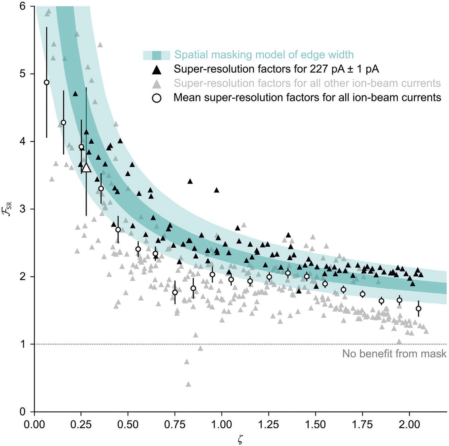
Super-resolution. Plot showing lateral super-resolution factor, , as a function of the ratio of milling depth to mask thickness, ζ. The light and dark regions of cyan respectively indicate the 95% coverage interval and the interval between the lower and upper quartiles of the spatial masking model. The black triangles represent all features below the zero plane that we mill with an ion-beam current of 227 ± 1 pA. The white triangle corresponds to a representative feature with a depth of 18 nm and edge widths that decrease from 195 ± 18 nm before removal of the mask to 54 ± 12 nm after, yielding a super-resolution factor of 3.6 +1.2/−0.7. The black bars above and below the white triangle indicate the distribution width of super-resolution factor as a 95% coverage interval. The distribution width in the ζ direction of ± 0.01 is smaller than the data marker. The gray triangles represent features that we mill with all other ion-beam currents, which range from approximately 80 to 800 pA. The white circles represent a subset of mean super-resolution factors from the entire data set, with downsampling for clarity. The black bars indicate uncertainties of mean super-resolution factor as 95% coverage intervals. Uncertainties of ζ are smaller than the data markers. More details are in Figures S8 and S13 and Table S8 (Supporting Information).
Beyond this primary comparison of theory and experiment, two variants of our spatial masking model allow secondary tests of its reliability. The first variant models the milling of a single line, matching that of an experimental study that achieved super-resolution at the scale of one to ten nanometers.[5b] This line variant fits the experimental data with and extracts reasonable parameter values from decreasing widths of nanochannels in quartz, resulting from line scans of a focused ion beam through sacrificial chromium masks of increasing thickness (Note S7 and Figure S14, Supporting Information). The second variant models the pattern of lines and spaces of variable pitch and duty cycle, simulating a conventional structure to test resolution, albeit with edge profiles that are characteristic of focused-ion-beam milling. This line-space variant shows trends that are comparable to our experimental results (Figures S15 and S16, Supporting Information), indicating that reductions in edge width translate to improvements of the conventional resolution metric of line-space density or half-pitch of periodic features.
The general agreement of our spatial masking model, various experimental results, and test-structure simulations substantiates our theory as a useful construct, which we extend into the temporal domain to explore the limits of the process of spatial masking.
2.4.3. Temporal Efficiency
Having demonstrated the capability of our analytic model to describe generally the spatial advantage of a sacrificial mask, we extend the model into the temporal domain to investigate the temporal efficiency of the fabrication process. We argue that spatial masking is rational under two conditions—first, if patterning with a high value of ion-beam current through a sacrificial mask requires less time than patterning with a low value of ion-beam current directly into the substrate, and second, if the patterning resolution at a minimal value of ion-beam current, typically around 1 pA for commercial systems at the state of the art, exceeds critical dimensions of the nanostructure design. The temporal efficiency of spatial masking, ητ, describes the extent to which patterning with a high value of ion-beam current through a sacrificial mask to achieve a certain effective lateral resolution saves time,
| (4) |
where Vs and Vm are, respectively, the volumes of the substrate and mask that the ion beam mills (Note S8, Supporting Information). For simplicity, we neglect the time to deposit and remove the sacrificial mask, which is a fraction ranging from 10−3 to 10−1 of the time to mill with a low value of ion-beam current. Equation (4) predicts that the temporal efficiency of spatial masking increases as physical selectivity increases and decreases as milling depth increases with respect to mask thickness (Figure 7a). Moreover, Equation (4) implies that the limits of milling depth for spatial masking occur where the temporal efficiency falls below unity. Solving for this condition numerically reveals that the efficiency limit is proportional to the physical selectivity of the mask and substrate (Figure 7b). Applying this model, while accounting for all measurement uncertainties, yields a remarkable prediction for our bilayer patterning a nanostructure with a certain edge width, using a high value of ion-beam current through a sacrificial mask, would require less time than directly milling a similar nanostructure with a low value of ion-beam current to depths ranging from 35 to 135 times the thickness of the chromia mask, or approximately 2 to 9 μm. In this way, even modest improvements in physical selectivity yield relatively large improvements in the milling range, ζmax. To better understand the intriguing implication of these results, we combine our experimental measurements of super-resolution factors with experimental values of temporal efficiency and revisit the resolution-throughput tradespace.
Figure 7.
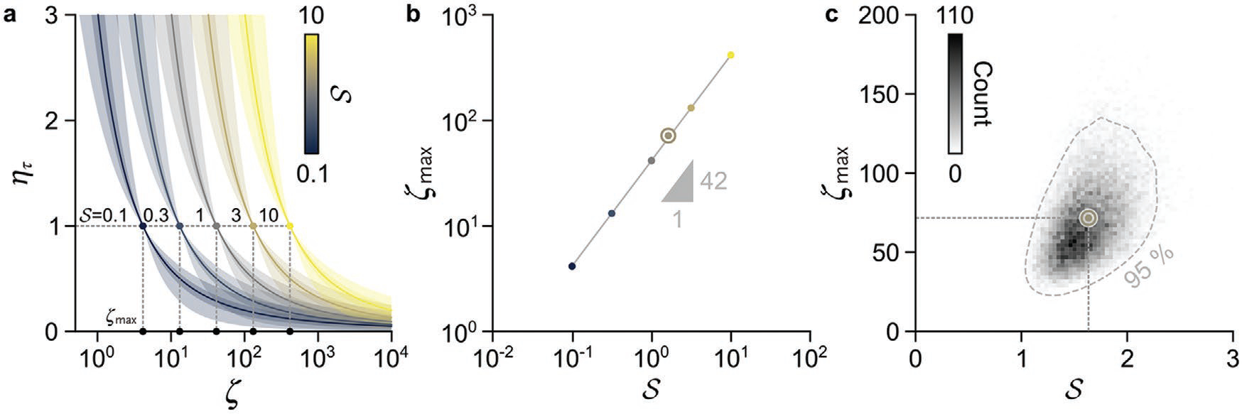
Temporal efficiency. a) Plots showing theoretical mean values of temporal efficiency, ητ, as a function of milling depth for a range of values of physical selectivity, S, and a scaling exponent of 0.15 +0.06/−0.07. For clarity, we consider uncertainty only from the scaling exponent. The light and dark regions respectively indicate the 95% coverage interval and the interval between the lower and upper quartiles of temporal efficiency. The circles are positions of maximum milling depth, where the temporal milling efficiency equals unity. b) Plot showing maximum milling depth, ζmax, as a function of physical selectivity. The circles correspond to theoretical values of maximum milling depth in (a). Uncertainties of the data, which are 95% coverage intervals of the mean values, are smaller than the data markers. c) Joint histogram showing physical selectivity and maximum milling depth with (dash line) contour indicating the 95% coverage region. The roundels in (b,c) correspond to our experimental values that predict a maximum milling depth at which super-resolution patterning remains temporally efficient, ζmax, of 71+64/−36.
2.4.4. Paradigm Shift
Lithographic patterning has a characteristic tradespace,[12a] with lateral resolution following a power-law dependence on areal throughput for different processes. The tradespace of focused-ion-beam milling is analogous but requires consideration of volume throughput. A key finding of our study is that a sacrificial mask transforms the coupling of lateral resolution and volume throughput. This is evident in the improvement of conventional resolution to super-resolution by factors of 1.8 to 2.7 after removal of the mask. These experimental results are independent of our theoretical model of super-resolution (Figure 8a). Power-law models of each resolution–throughput trend enable evaluation of the tradespaces to determine equivalent values of conventional resolution and super-resolution but dramatically different values of volume throughput resulting from different ion-beam currents (Table S13 and Note S6, Supporting Information). A minimal extrapolation of experimental values of volume throughput for equivalent values of conventional resolution and super-resolution indicates an improvement by a factor of 42 ± 2 for our highest value of ion-beam current. Extrapolation to lower values of ion-beam current implies even more impressive improvements, ranging from two to three orders of magnitude (Table S13, Supporting Information), while extrapolation to higher values of ion-beam current suggests potential limits of such improvements. To better understand the spatiotemporal advantages of spatial masking, we combine metrics of lateral resolution and volume throughput to empirically investigate this limiting behavior.
Figure 8.
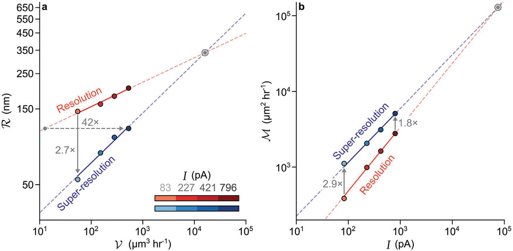
Lateral resolution and volume throughput. a) Plots showing lateral resolution, R, which can be either (red) conventional resolution or (blue) super-resolution as a function of volume throughput, V. The horizontal dash arrow indicates a factor of improvement of 42 in volume throughput for an equal value of lateral resolution with minimal extrapolation outside of our experimental range. The vertical solid arrow indicates a mean factor of improvement of 2.7 in resolution for the volume throughput that corresponds to our lowest value of ion-beam current. b) Plots showing figures of merit, M, as a function of ion-beam current, I (red) before and (blue) after removal of the chromia mask. The vertical arrows indicate mean factors of improvement in figure of merit of 2.9 for our lowest value of ion-beam current and 1.8 for our highest value of ion-beam current. For both plots, solid lines are fits of power-law models to experimental data, dash lines extrapolate outside of the experimental range, roundels mark the intersection of conventional resolution and super-resolution trends, and uncertainties are smaller than data markers.
We introduce a figure of merit, , as a function of ion-beam current to elucidate the effect of spatial masking on the tradespace of lateral resolution, , and volume throughput, ,
| (5) |
The figure of merit, in units of μm2 h−1, increases as ion-beam current increases, decreases as resolution degrades, and collapses to in the absence of a sacrificial mask, where equals unity. In this way, the figure of merit enables direct comparison of conventional milling of a bilayer before removal of the sacrificial mask, to super-resolution milling through a sacrificial mask after removal. For our experimental system, the mask increases the figure of merit by a factor ranging from 1.8 to 2.9, due to better resolution with a mean factor of 2.1 ± 0.9 at a constant volume throughput (Figure 8b and Table S13, Supporting Information). Extrapolation to low values of ion-beam current suggests higher factors of improvement, whereas extrapolation to high values of ion-beam current implies a limit to improvement by a sacrificial mask.
Equation (5) yields two nonobvious insights into the effects of physical selectivity and milling depth on process quality (Figure S17, Supporting Information). First, our model predicts that, for a constant value of milling depth, figure of merit increases as physical selectivity decreases. This implies that softer masks hasten the milling process, improving volume throughput with little cost to lateral super-resolution but some cost to milling range. Second, our model predicts that, for a constant physical selectivity, figures of merit increase as milling depth decreases. This implies that thicker masks yield nanostructures with narrower edges than thinner masks, improving lateral resolution and milling range with some cost to volume throughput. Other bilayer materials might optimize physical selectivity for particular objectives. These new insights into the resolution–throughput tradespace motivate experimental tests of the improvements in volume throughput that sacrificial masking enables.
2.5. Lens Array Fabrication
Our new understanding of the resolution–throughput tradespace of focused-ion-beam machining predicts that sacrificial masking can increase the throughput of device fabrication at a higher value of ion-beam current. This improvement of throughput is relative to equivalent devices resulting from directly milling a workpiece at a lower value of ion-beam current. To test this prediction, we mill two arrays of Fresnel lenses that are nominally equivalent, either a single lens directly into silica with an ion-beam current of 26 pA, or 75 lenses through a sacrificial mask of chromia and into silica with an ion-beam current of 2600 pA, in an equal time of 3.75 h. Without a chromia mask to dissipate the accumulation of positive charge,[17b] direct milling of silica requires a modification of the fabrication process, such as simultaneous exposure by an electron beam or flood gun, which may or may not be available, to neutralize the accumulation of positive charge and achieve comparable results (Table S14, Supporting Information). We perform a control experiment to test this effect, milling single lenses directly into silica at an ion-beam current of 2600 pA, with and without simultaneous exposure by an electron beam. Fresnel lenses are simple to design[35] but their structural complexity and sharp transitions in surface relief make them challenging to machine and measure at small scales.[36] For both reasons, Fresnel lenses are suitable targets for novel fabrication and functional characterization. In testing the dose delivery to fabricate the Fresnel lenses, we develop methods to trim the dose around the peaks of concentric ridges to tune the super-resolution effect, and to exhaust the mask in the milling process (Note S10, Supporting Information).
In our application, the function of Fresnel lenses is to focus incident light into spots of a certain size at a certain distance away from the surface of a microscope coverslip, enabling projection standards for, and functional characterization by, optical microscopy. These primary metrics of performance are nearly equivalent for both lens arrays. The single lens that we mill directly into silica at an ion-beam current of 26 pA and with electron-beam exposure to achieve the best results serves as a reference. In comparison, the projection distances of the lenses that we mill through chromia are equal to within 0.14% +1.4%/−1.6% and the apparent spot sizes are equal to are equal to within −0.27%+0.88%/−0.78% (Figure 9 and Figure S19, Supporting Information). In this way, the reference lens and lens array perform similarly as projection standards. In contrast, the projection distances and apparent spot sizes of the two control lenses differ significantly from the reference lens. Direct milling into silica at an ion-beam current of 2600 pA with electron-beam exposure results in a lens with a projection distance that differs by 3.46% +3.27%/−3.14% and an apparent spot size that differs by 14.38% +0.04%/−0.04% from the reference lens (Figure S20 and Table S14, Supporting Information). Without the electron beam, charge accumulation severely impairs the milling process, degrading the quality of the resulting lens structure so much as to compromise its performance. There is also a 30% to 40% reduction in the transmittance of the lenses that we mill through chromia, which is potentially attributable to the intermixing of chromia and silica and potentially remediable by pattern transfer to an optical polymer.[37] The similar performance of the reference lens and the lens that we mill through chromia demonstrates an improvement in fabrication throughput by a factor of 75, testing the new tradespace and showing a significant benefit from the paradigm shift.
Figure 9.
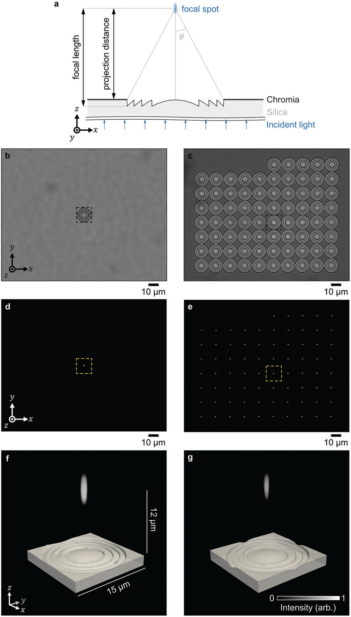
Fresnel lens arrays. a) Schematic showing the design of a single Fresnel lens. b,c) Brightfield optical micrographs showing Fresnel lenses that we mill b) directly into silica with an ion-beam current of 26 pA and c) through chromia and into silica with an ion-beam current of 2600 pA. Different background intensities result from the absence or presence of chromia. d,e) Brightfield optical micrographs showing focal spots from the lenses in (b,c). f,g) Volume reconstruction of the focal spots from brightfield optical micrographs that we register to surface reconstructions from atomic force micrographs of the Fresnel lenses in (b,c).
3. Conclusions
Focused-ion-beam machining occurs within a tradespace of lateral resolution and volume throughput. At the root of this tradespace is a power-law dependence of lateral resolution on ion-beam current, such that fine features mill slowly. This limits the utility of what is otherwise a powerful process to directly form complex nanostructures without serial lithography, yielding the conventional view of the focused ion beam as that of a machine tool for prototyping rather than for manufacturing. In this study, we comprehensively and systematically investigate how a sacrificial mask can radically improve the resolution–throughput tradespace, using a chromia film to mask a silica substrate from gallium ions. Chromia proves to be a multifunctional mask, facilitating in-line metrology of ion-beam focus without issues from dielectric charging, enabling theoretical and experimental studies of the super-resolution effect, and being chemically suitable for a variety[23a] of processes and applications. This general process may extend to other bilayer materials and ion sources. Building on our characterization and application of these useful properties, we develop foundational theory for the spatial masking process and super-resolution effect, deriving an analytic model that generally predicts our experimental results and provides key insight into the parameter space of the process. Our tractable theory informs a paradigm shift from empirical to engineering design of masking and milling processes. Through measurements that are independent of our model and its simplifying approximations, we experimentally demonstrate super-resolution factors of up to 6 ± 2, and improvements to volume throughput of at least factors of 42 ± 2 for our smallest mean super-resolution factor and with minimal extrapolation. For our larger super-resolution factors, further extrapolation to equal values of resolution at lower values of ion-beam current implies a higher volume throughput by two to three orders of magnitude. An effect of this scale is analogous to the gain mechanism of chemical amplification of resist materials, in which effective thresholding improves contrast in photolithography, or increases in sensitivity improve areal throughput of electron-beam lithography.[38] We test these predictions by the fabrication of Fresnel lenses, increasing throughput by a factor of 75 for functionally equivalent lenses that we mill through chromia and into silica relative to lenses that we mill directly into silica. Further work could develop the Fresnel lens array into a novel standard for projecting focal spots into a sample to perform magnification and distortion calibration in the presence of sample aberrations.[39] Further work is also necessary to explore this advantage and optimize the tradespace for different objectives, such as fabricating other types of diffractive optics,[36c] electromagnetic metasurfaces,[40] or nanofluidic molds.[11,41] However, our results show a temporal advantage that is so decisive as to enable a paradigm shift from conventional machining to ultrarapid prototyping of complex structures for research and development, and even to commercial manufacturing of device arrays that would conventionally require hundreds to thousands of hours of machine time. Moreover, our chromia characterization and model development can impact sample preparation for materials characterization[6] and biological imaging,[7] enabling prediction and optimization of the super-resolution and volume throughput that are latent to masking and milling processes for volumetric imaging. In general, our new insights into the resolution–throughput tradespace extend the utility of focused-ion-beam machining from fundamental science to commercial products.
4. Experimental Section
Fabrication:
To form the chromia-silica bilayer, thermal oxidation of p-type silicon substrates produced a silica working film, over which sputter deposition yielded a chromia masking film. An electron–ion beam system focused gallium cations from a liquid metal source onto the bilayer, at an accelerating voltage of 30 kV, and with ion-beam currents that ranged from approximately 26 to 2600 pA (Table S2, Supporting Information). Milling of the bilayer occurred at the eucentric height of the electron–ion beam system, at normal incidence to the ion-beam column, and with the stage tilted at 0.9075 rad (52°) with respect to the electron-beam column. Arrays of pits tested the focus of the ion beam, and arrays of squares in a checkerboard pattern tested the spatial masking process. After milling and characterization of these test structures, immersion in chromium etchant selectively removed the chromia mask from the silica film.
Fresnel lenses milled into silica coverslips required several variations of the machining process. Bulk milling rates of chromia and silica and the film thickness of chromia informed the estimation of ion doses needed to mill the Fresnel lenses. Interpolation of ion dose as a function of radial position yielded ion doses for milling positions in a Cartesian coordinate system. One reference Fresnel lens milled directly into silica, with an ion-beam current of approximately 26 pA in a time of 3.75 h, required scanning the electron beam over the patterning area at a nominal electron-beam current of 100 pA to neutralize the accumulation of positive charge from ion irradiation. Two control Fresnel lenses milled directly into silica, with an ion-beam current of approximately 2600 pA in a time of 0.04 h, one lens with and one lens without a nominal electron-beam current of 6400 pA, tested the effect of charge neutralization. Sputter deposition of a chromia film onto a silica coverslip enabled the milling of an array of 75 Fresnel lenses, with an ion-beam current of approximately 2600 pA in a time of 3.75 h, for a comparison of lens performance against the reference Fresnel lens.
Characterization:
Ellipsometry quantified the thickness of silica films. Ellipsometry, transmission electron microscopy, and X-ray diffractometry quantified the thickness of chromia films.
Atomic force microscopy characterized the surface topography of all structures resulting from focused-ion-beam milling. Surface probes were silicon nitride cantilevers with nominal values of a length of 27 μm, a resonant frequency of 1400 kHz, and a force constant of 17 N m−1. Probe tips were silicon with nominal values of a front angle of 261 ± 44 mrad (15° ± 2.5°), a back angle of 446 ± 44 mrad (25° ± 2.5°), a radius of 5 nm, and a maximum radius of 12 nm.
X-ray diffractometry characterized several properties of silica and chromia. The incident X-rays, which resulted from copper Kα transitions, had an energy of 1.29 fJ (8.04 keV) and a wavelength of 0.1506 nm. Fits of a reflectivity model[26] to the resulting X-ray data yielded measurements of density, surface roughness, and thickness. All fits of models to data were by damped least-squares estimation with uniform weighting. The Scherrer equation estimated crystallite size from X-ray diffraction data.
Scanning electron microscopy characterized chromia surfaces and test pits milled into the chromia-silica bilayer, and Fresnel lenses milled through a chromia film and into a silica coverslip. The electron beam had an acceleration voltage of 5 kV and a nominal current of 100 pA, and impinged on the sample from a working distance of 4.2 mm, at normal incidence for the chromia surface and test pits, and at an incident angle of 0.9075 rad (52°) for Fresnel lenses. Signals in all scanning electron micrographs resulted from secondary electrons incident on a through-lens detector.
Brightfield optical microscopy quantified the projection distances and apparent spot sizes of the Fresnel lenses. The microscope objective lens and tube lens pair had a nominal magnification of 50× and a numerical aperture of 0.95. The optical microscope operated in trans-illumination at wavelengths that ranged from 420 to 510 nm with a peak wavelength of approximately 460 nm. An array of subwavelength apertures with a pitch of 5001.45 ± 1.08 nm calibrated[42] the mean pixel size of all optical micrographs as 126.82 ± 0.03 nm. Scanning vertically through focus in increments of approximately 40 nm resulted in a series of optical micrographs that included each lens and spot within a focal volume of approximately 258 by 258 by 40 μm. The vertical positions of best focus of the lens surface corresponded to the maxima of ninth-order polynomial models of image contrast. The vertical positions of best focus of each spot corresponded to maxima of ninth-order polynomial models of the apparent standard deviations of symmetric bivariate Gaussian models of the spot images. The difference between the two vertical positions of best focus yielded the projection distance of each lens.
In-line Resolution Metrology:
Correlative measurements of test pits by scanning electron microscopy and by atomic force microscopy enabled evaluation of pit radius by scanning electron microscopy, as a measure of effective lateral resolution just prior to the fabrication of complex test structures. Maximum signal intensities in scanning electron micrographs correlated with the negative of the second derivative of pit surface topography from atomic force micrographs, the latter of which required second-order differentiation with respect to lateral position. Monte-Carlo simulations of either microscopy measurement propagated uncertainties for each measurand (Note S4, Table S3, Supporting Information).
Milling Responses:
Analysis of leveled atomic force micrographs yielded measurements of the depth, surface roughness, and edge width of square features in checkerboard test patterns. Monte-Carlo simulations of these measurements propagated uncertainties for each measurand (Table S3, Supporting Information). Fits of error function models to the z position zbefore(s) of the surfaces in sections of atomic force micrographs extracted parameter values of the depth and edge width of features before chromia removal, Equation (6),
| (6) |
Fits of truncated error function models to the z position zafter(s) of the surfaces in sections of atomic force micrographs extracted parameter values of the depth and edge width of the same features after chromia removal, Equation (7),
| (7) |
In Equations (6) and (7), d is the depth of the feature, s0 is the location of the edge, σedge is the standard deviation of the Gaussian function, and c is a constant. In this analysis, edge widths from the 95% coverage intervals of the widths of the error functions corresponded to wbefore = 4σedge before removal of the chromia and wafter = 2σedge after removal of the chromia. Repeated measurements along the edges of each square feature in the checkerboard test patterns fully sampled the test patterns.
Ion Penetration:
Three simulations of ion penetration into the bilayer, using Stopping and Range of Ions in Matter (SRIM) software, elucidated the responses of the material system to ion irradiation (Table S7, Supporting Information).[20] Material densities, elemental compositions, and three different chromia thicknesses were key input parameters in these simulations. The three chromia thicknesses were 63.5 nm, which corresponded to milling bulk chromia, 16 nm, which corresponded to the z position at which the chromia-silica interface evidently began to influence the milling response of chromia, and 0 nm, which corresponded to milling bulk silica. In each Monte-Carlo simulation, 105 gallium ions, each with a landing energy of 4.81 fJ (30 keV), bombarded either a chromia-on-silica target or a silica target at normal incidence. The resulting spatial distributions of gallium ions in the target materials guided interpretation of the nanostructure topographies that were apparent in atomic force micrographs.
Spatial Masking:
Theoretical analysis of the spatial profiles of ion doses yielded an analytic expression for super-resolution factors. These one-dimensional profiles corresponded to the ion doses required to mill a uniform region through a sacrificial mask and into an underlying substrate. For simplicity, this analysis assumed that the mask had an average milling rate and a thickness zm, and that the substrate had an average milling rate and a final depth zs. A Gaussian approximation of the distribution of current density of the ion beam led to a model of the spatial profile of the ion dose along the x direction, D(x), in terms of an error function of the form,
| (8) |
where D0 is the dose of the ion beam, x0 is the center position of the edge of the pattern, and σ is the effective standard deviation of the Gaussian profile of the ion beam. The dose required to mill through the mask and to a depth, zs, into the substrate is the sum of the dose required to mill through the mask, Dm, and the dose required to mill the nanostructure, Ds. Accordingly, . Milling depths, zm and zs, have units of length, and milling rates, and , have units of volume per current per second or μm3 nA−1 s−1. The quotient of measurements of length and milling rate yields a value with units of dose, nA s μm−2, which reduces to pC μm−2.
The lateral extent to which the ion beam milled the underlying silica film corresponds to the x position of the dose in Equation (8) that exceeded the dose required to mill through the mask. In other words, the x position at which the mask began to screen the tail of the ion beam occurred where D(x) = D(xm) = Dm (Figure S12, Supporting Information),
| (9) |
Two dimensionless parameters simplified Equation (9)—the ratio of the milling depth of the substrate to the thickness of the mask, , and the ratio of the milling rate of the substrate to the milling rate of the mask, , which is the physical selectivity. Making these substitutions in Equation (9) and solving the resulting expression for xm yielded the position at which the mask began screening the tail of the ion beam,
| (10) |
The super-resolution factor is the ratio of the edge width that resulted from a low value of ion-beam current, wlow, to the edge width that resulted from a high value of ion-beam current, whigh, after removal of the sacrificial film. The 95% coverage interval of the error function widths defined the nanostructure edge widths. These widths extended to ± 2σlow on either side of the center position of the edge that resulted from low current, where σlow is the effective standard deviation of the Gaussian profile of the beam resulting from a low current. Similarly, the extents of the edge that resulted from high current before removal of the sacrificial film were ± 2σhigh, but after removal of the sacrificial mask, the edge width decreased from 4σhigh to a final width of . The ratio of widths from either case yielded the super-resolution factor, which is valid for ,
| (11) |
| (12) |
and
| (13) |
Application of the experimental constraint of sparse and discontinuous values of ion-beam current to Equation (13) highlighted the effect of removal of the sacrificial mask on edge width. A single value of ion-beam current constrained the parameters, σlow = σhigh = σ, which isolated the effect of the mask on the edge profiles and yielded an expression that is applicable to the experimental system,
| (14) |
Line–Space Patterns:
Simulations of the focused-ion-beam milling of periodic lines and spaces elucidated the limitations of the process to form dense arrays in the presence and absence of a sacrificial mask (Figures S15 and S16, Supporting Information). Application of the vertical milling response of the bilayer predicted structures resulting from patterns of ion dose with pitch, p, ranging from 1σ to 10σ and duty cycle, δ, ranging from 0% to 100%. For each set of parameters, the bilayer model predicted vertical profiles in silica that could result from either direct exposure, zdirect(x),
| (15) |
where msilica is the milling rate of bulk silica and Dls(x) is a spatial pattern of ion dose resulting from positioning a Gaussian ion beam with standard deviation σ, to form lines and spaces of design depth, ζdesign – or from milling through a sacrificial mask, zmasking(x),
| (16) |
where mbilayer is the milling rate of the chromia and silica bilayer. Both simplifications neglected the dependence of incidence angle on milling rate, any effects of redeposition, and any defocus of the ion beam due to charge accumulation. The fraction of predicted depth to designed depth defined a metric of fabrication feasibility. A tolerance of 0.975 identified values of a minimum pitch at which patterning was feasible and enabled the comparison of values of minimum pitch for direct milling and milling in the presence of a sacrificial mask.
Temporal Efficiency:
Equation (4) yielded theoretical values of temporal efficiency as a function of milled depth after normalization by mask thickness and as a function of physical selectivity (Note S8, Supporting Information). Monte-Carlo simulations propagated uncertainties from physical selectivity and of the scaling exponent of the effective lateral patterning resolution from fits of a power law model to edge widths as a function of ion-beam current (Table S3, Supporting Information). These simulations yielded values of temporal efficiency for ζ that ranged from 10−1 to 104 and enabled the calculation of values of milling depth where ητ = 1 by interpolation to define maximum milling depths for five mean values of physical selectivity that ranged from 0.1 to 10. Repeating this simulation 104 times yielded distributions of maximum milling depth. Similarly, the analytic expression for temporal efficiency and propagation of uncertainties from atomic force microscopy, normal distributions of mask thickness, uncertainties from physical selectivity, and of the exponent of the power-law model of effective lateral patterning resolution, yielded distributions of maximum milling depth of the bilayer (Table S11, Table S3, Supporting Information). Kernel density estimation[43] with a Gaussian kernel estimated the joint probability density of physical selectivity and maximum milling depth.
Throughput:
Values of volume throughput for equivalent values of resolution and super-resolution required two steps of calculation. First, power-law models fit experimental values of resolution or super-resolution as a function of volume throughput by damped least-squares estimation with uniform weighting. Second, setting the power-law model of the resolution trend equal to each value of super-resolution and inverting the resolution model enabled the calculation of corresponding values of equivalent throughput, which required extrapolating somewhat outside of the range of experimental values (Table S13, Supporting Information).
Supplementary Material
Acknowledgements
The authors acknowledge helpful comments from Lindsay C. C. Elliot, Henri J. Lezec, Jacob M. Majikes, and Adam L. Pintar, and inspiration on silicate formation from Sven Larsen. A.C.M. acknowledges support of a National Research Council Research Associateship. S.M.S. supervised the study. A.C.M. and S.M.S. designed the study with contributions from all authors. K.-T.L. prepared silica substrates. B.R.I. optimized the deposition of chromia. A.C.M. performed atomic force microscopy. A.C.M. and K.S. performed X-ray diffraction experiments and analysis. K.S. performed transmission electron microscopy. A.C.M., J.S.V., and S.M.S. developed the in-line metrology method. A.C.M. and J.S. performed focused-ion-beam milling and scanning electron microscopy. A.C.M. and S.M.S. performed SRIM simulations. A.C.M., J.S.V., and S.M.S. developed the theoretical model of super-resolution. A.C.M. and S.M.S. designed the Fresnel lenses. C.R.C. and A.C.M. performed optical microscopy. A.C.M. and S.M.S. designed the statistical analysis and prepared the manuscript with contributions from all authors.
Footnotes
Conflict of Interest
The authors declare no conflict of interest.
Supporting Information
Supporting Information is available from the Wiley Online Library or from the author.
Contributor Information
Andrew C. Madison, Microsystems and Nanotechnology Division, National Institute of Standards and Technology, Gaithersburg, MD 20899, USA
John S. Villarrubia, Microsystems and Nanotechnology Division, National Institute of Standards and Technology, Gaithersburg, MD 20899, USA
Kuo-Tang Liao, Microsystems and Nanotechnology Division, National Institute of Standards and Technology, Gaithersburg, MD 20899, USA; Maryland Nanocenter, College Park, MD 20740, USA.
Craig R. Copeland, Microsystems and Nanotechnology Division, National Institute of Standards and Technology, Gaithersburg, MD 20899, USA
Joshua Schumacher, CNST NanoFab, National Institute of Standards and Technology, Gaithersburg, MD 20899, USA.
Kerry Siebein, CNST NanoFab, National Institute of Standards and Technology, Gaithersburg, MD 20899, USA.
B. Robert Ilic, Microsystems and Nanotechnology Division, National Institute of Standards and Technology, Gaithersburg, MD 20899, USA; CNST NanoFab, National Institute of Standards and Technology, Gaithersburg, MD 20899, USA.
J. Alexander Liddle, Microsystems and Nanotechnology Division, National Institute of Standards and Technology, Gaithersburg, MD 20899, USA.
Samuel M. Stavis, Microsystems and Nanotechnology Division, National Institute of Standards and Technology, Gaithersburg, MD 20899, USA
Data Availability Statement
The data that support the findings of this study are available from the corresponding author upon reasonable request.
References
- [1].Ocola LE, Rue C, Maas D, MRS Bull. 2014, 39, 336. [Google Scholar]
- [2].a) Blaikie A, Miller D, Alemán BJ, Nat. Commun. 2019, 10, 4726; [DOI] [PMC free article] [PubMed] [Google Scholar]; b) Xu T, Walter EC, Agrawal A, Bohn C, Velmurugan J, Zhu W, Lezec HJ, Talin AA, Nat. Commun. 2016, 7, 10479; [DOI] [PMC free article] [PubMed] [Google Scholar]; c) Ahmed R, Victora RH, Appl. Phys. Lett. 2018, 112, 182401; [Google Scholar]; d) Lee SC, Neumann A, Jiang YB, Artyushkova K, Brueck SRJ, Nanotechnology 2016, 27, 375707. [DOI] [PubMed] [Google Scholar]
- [3].a) Chen M, Pethö L, Sologubenko AS, Ma H, Michler J, Spolenak R, Wheeler JM, Nat. Commun. 2020, 11, 2681; [DOI] [PMC free article] [PubMed] [Google Scholar]; b) Cho H, Kim J, Park H, Won Bang J, Seop Hyun M, Bae Y, Ha L, Yoon Kim D, Min Kang S, Jung Park T, Seo S, Choi M, Suh K-Y, Nat. Commun. 2014, 5, 3137. [DOI] [PubMed] [Google Scholar]
- [4].a) Dhawan A, Gerhold M, Madison A, Fowlkes J, Russell PE, Vo-Dinh T, Leonard DN, Scanning 2009, 31, 139; [DOI] [PubMed] [Google Scholar]; b) Zhu W, Xu T, Wang H, Zhang C, Deotare PB, Agrawal A, Lezec HJ, Sci. Adv. 2017, 3, e1700909; [DOI] [PMC free article] [PubMed] [Google Scholar]; c) Chen P, Jung IW, Walko DA, Li Z, Gao Y, Shenoy GK, López D, Wang J, Nat. Commun. 2019, 10, 1158; [DOI] [PMC free article] [PubMed] [Google Scholar]; d) Bassim ND, Giles AJ, Ocola LE, Caldwell JD, Appl. Phys. Lett. 2018, 112, 091101. [Google Scholar]
- [5].a) Liao K-T, Schumacher J, Lezec HJ, Stavis SM, Lab Chip 2018, 18, 139; [DOI] [PMC free article] [PubMed] [Google Scholar]; b) Menard LD, Ramsey JM, Nano Lett. 2011, 11, 512; [DOI] [PMC free article] [PubMed] [Google Scholar]; c) Zhou J, Wang Y, Menard LD, Panyukov S, Rubinstein M, Ramsey JM, Nat. Commun. 2017, 8, 807; [DOI] [PMC free article] [PubMed] [Google Scholar]; d) Fanzio P, Mussi V, Manneschi C, Angeli E, Firpo G, Repetto L, Valbusa U, Lab Chip 2011, 11, 2961. [DOI] [PubMed] [Google Scholar]
- [6].a) Cao S, Tirry W, Van Den Broek W, Schryvers D, Microsc J. 2009, 233, 61; [DOI] [PubMed] [Google Scholar]; b) Giannuzzi LA, Stevie FA, Micron 1999, 30, 197; [Google Scholar]; c) Nellen PM, Callegari V, Sennhauser U, Chimia 2006, 60, 735. [Google Scholar]
- [7].Narayan K, Subramaniam S, Nat. Methods 2015, 12, 1021. [DOI] [PMC free article] [PubMed] [Google Scholar]
- [8].Orloff J, Utlaut M, Swanson L, High Resolution Focused Ion Beams: FIB and Its Applications, Kluwer Academic/Plenum Publishers, New York, NY: 2003. [Google Scholar]
- [9].Vladov N, Segal J, Ratchev S, J. Vac. Sci. Technol., B: Microelectron. Nanometer Struct.–Process., Meas., Phenom. 2015, 33, 041803. [Google Scholar]
- [10].a) Freeman D, Luther-Davies B, Madden S, TechConnect Briefs 2006, 3, 241; [Google Scholar]; b) Holzer L, Indutnyi F, Gasser PH, Münch B, Wegmann M, J. Microsc. 2004, 216, 84. [DOI] [PubMed] [Google Scholar]
- [11].Liao K-T, Madison AC, Pintar AL, Ilic BR, Copeland CR, Stavis SM, arXiv:2101.03881 [cond-mat.soft], arXiv 2020. [Google Scholar]
- [12].a) Marrian CRK, Tennant DM, J. Vac. Sci. Technol., A 2003, 21, S207; [Google Scholar]; b) Mack CA, Proc. SPIE 2019, 10958, 10.1117/12.2517598.full?SSO=1. [DOI] [Google Scholar]
- [13].Liddle JA, Gallatin GM, ACS Nano 2016, 10, 2995. [DOI] [PMC free article] [PubMed] [Google Scholar]
- [14].a) Wu H, Stern LA, Xia D, Ferranti D, Thompson B, Klein KL, Gonzalez CM, Rack PD, J. Mater. Sci.: Mater. Electron. 2014, 25, 587; [Google Scholar]; b) Tan S, Livengood R, Hack P, Hallstein R, Shima D, Notte J, McVey S, J. Vac. Sci. Technol. B 2011, 29, 06F604. [Google Scholar]
- [15].a) Córdoba R, Orús P, Strohauer S, Torres TE, De Teresa JM, Sci. Rep. 2019, 9, 14076; [DOI] [PMC free article] [PubMed] [Google Scholar]; b) Fumio A, Tomokazu K, Osamu M, Anto Y, Shingo Y, Koichi K, Hiroyuki M, Naoya H, Proc. SPIE 2014, 9235, 92350F. [Google Scholar]
- [16].a) Kannegulla A, Cheng L-J, Nanotechnology 2016, 27, 36LT01; [DOI] [PubMed] [Google Scholar]; b) Vermeij T, Plancher E, Tasan CC, Ultramicroscopy 2018, 186, 35; [DOI] [PubMed] [Google Scholar]; c) Taillon JA, Ray V, Salamanca-Riba LG, Microsc. Microanal. 2017, 23, 872; [DOI] [PubMed] [Google Scholar]; d) Qu M, Shen Y, Wu L, Fu X, Cheng X, Wang Y, Precis. Eng. 2020, 62, 10. [Google Scholar]
- [17].a) Alias MS, Liao H-Y, Ng TK, Ooi BS, J. Vac. Sci. Technol. B 2015, 33, 06F701; [Google Scholar]; b) Stokes DJ, Vystavel T, Morrissey F, Phys J. D: Appl. Phys. 2007, 40, 874; [Google Scholar]; c) Komoda H, Yoshida M, Yamamoto Y, Iwasaki K, Nakatani I, Watanabe H, Yasutake K, Microelectron. Reliab. 2006, 46, 2085; [Google Scholar]; d) Komoda H, Nakatani I, Watanabe H, Yasutake K, Jpn. J. Appl. Phys. 2005, 44, 7907; [Google Scholar]; e) Gervinskas G, Seniutinas G, Juodkazis S, Laser Photonics Rev. 2013, 7, 1049. [Google Scholar]
- [18].a) Blom T, Welch K, Strømme M, Coronel E, Leifer K, Nanotechnology 2007, 18, 285301; [Google Scholar]; b) Ostadi H, Jiang K, Prewett PD, Microelectron. Eng. 2009, 86, 1021. [Google Scholar]
- [19].a) Kempshall BW, Schwarz SM, Prenitzer BI, Giannuzzi LA, Irwin RB, Stevie FA, J. Vac. Sci. Technol. B 2001, 19, 749; [Google Scholar]; b) Urbánek M, Uhlíř V, Bábor P, Kolíbalová E, Hrnčíř T, Spousta J, Šikola T, Nanotechnology 2010, 21, 145304. [DOI] [PubMed] [Google Scholar]
- [20].Ziegler JF, Ziegler MD, Biersack JP, Nucl. Instrum. Methods Phys. Res., Sect. B 2010, 268, 1818. [Google Scholar]
- [21].a) Abdullah MM, Rajab FM, Al-Abbas SM, AIP Adv. 2014, 4, 027121; [Google Scholar]; b) Julkarnain MD, Hossain J, Sharif KS, Khan KA, J. Optoelectron. Adv. Mater. 2011, 13, 485; [Google Scholar]; c) Ku RC, Winterbottom WL, Thin Solid Films 1985, 127, 241. [Google Scholar]
- [22].a) Hones P, Diserens M, Lévy F, Surf. Coat. Technol. 1999, 120–121, 277; [Google Scholar]; b) Khojier K, Savaloni H, Ashkabusi Z, Dehnavi NZ, Appl. Surf. Sci. 2013, 284, 489. [Google Scholar]
- [23].a) Aydinoglu F, Saffih F, Dey RK, Cui B, J. Vac. Sci. Technol. B 2017, 35, 06GB01; [Google Scholar]; b) Pang X, Gao K, Volinsky AA, J. Mater. Res. 2007, 22, 3531. [Google Scholar]
- [24].Ilic BR, Ray CH, Seibein K, Liddle JA, presented at The 61st Int. Conf. on Electron, Ion, and Photon Beam Technology and Nanofabrication, Orlando, FL June 2017. [Google Scholar]
- [25].Liddle JA, Salmassi F, Naulleau PP, Gullikson EM, J. Vac. Sci. Technol. B 2003, 21, 2980. [Google Scholar]
- [26].Yasaka M, Rigaku J. 2010, 26, https://www.rigaku.com/journal/summer-2010-volume-26-no-2/01-09. [Google Scholar]
- [27].Bhushan B, Thin Solid Films 1980, 73, 255. [Google Scholar]
- [28].a) Postek MT, Villarrubia JS, Vladár AE, J. Vac. Sci. Technol. B 2005, 23, 3015; [Google Scholar]; b) Villarrubia JS, Vladár AE, Postek MT, Surf. Interface Anal. 2005, 37, 951; [Google Scholar]; c) Reimer L, Scanning Electron Microscopy: Physics of Image Formation and Microanalysis, Springer, Berlin: 1985. [Google Scholar]
- [29].Villarrubia JS, Vladár AE, Ming B, Kline RJ, Sunday DF, Chawla JS, List S, Ultramicroscopy 2015, 154, 15. [DOI] [PubMed] [Google Scholar]
- [30].Mack C, Bunday B, Proc. SPIE 2016, 9778, 97780A. [Google Scholar]
- [31].a) Hagara M, Kulla P, Radioengineering 2011, 20, 516; [Google Scholar]; b) Lee SW, Lee SY, Pahk HJ, Curr. Opt. Photonics 2018, 2, 69. [Google Scholar]
- [32].Smith NS, Skoczylas WP, Kellogg SM, Kinion DE, Tesch PP, Sutherland O, Aanesland A, Boswell RW, J. Vac. Sci. Technol. B 2006, 24, 2902. [Google Scholar]
- [33].Xu X, Della Ratta AD, Sosonkina J, Melngailis J, J. Vac. Sci. Technol. B 1992, 10, 2675. [Google Scholar]
- [34].Han J, Lee H, Min B-K, Lee SJ, Microelectron. Eng. 2010, 87, 1. [Google Scholar]
- [35].Nishihara H, Suhara T, in Progress in Optics, Vol. 24 (Ed: Wolf E), Elsevier, Amsterdam: 1987, p. 1. [Google Scholar]
- [36].a) Chiu Y, Huang C-H, Hsu Y-C, presented at Optical Data Storage, Portland, Oregon: May 2007; [Google Scholar]; b) Fujita T, Nishihara H, Koyama J, Opt. Lett. 1982, 7, 578; [DOI] [PubMed] [Google Scholar]; c) Anna S, Andrzej M, Jacek M, Katarzyna K, Opt. Eng. 2017, 56, 057106. [Google Scholar]
- [37].Jacobo-Martín A, Jost N, Hernández JJ, Domínguez C, Vallerotto G, Askins S, Antón I, Rodríguez I, Opt. Express 2021, 29, 34135. [DOI] [PubMed] [Google Scholar]
- [38].a) Hiroshi I, Proc. SPIE 1999, 3678, 10.1117/12.350143; [DOI] [Google Scholar]; b) Reichmanis E, Houlihan FM, Nalamasu O, Neenan TX, Chem. Mater. 1991, 3, 394; [Google Scholar]; c) Gangnaik AS, Georgiev YM, Holmes JD, Chem. Mater. 2017, 29, 1898. [Google Scholar]
- [39].Copeland CR, Geist J, McGray CD, Aksyuk VA, Liddle JA, Ilic BR, Stavis SM, Light: Sci. Appl. 2018, 7, 31. [DOI] [PMC free article] [PubMed] [Google Scholar]
- [40].Hsiao H-H, Chu CH, Tsai DP, Small Methods 2017, 1, 1600064. [Google Scholar]
- [41].Campbell LC, Wilkinson MJ, Manz A, Camilleri P, Humphreys CJ, Lab Chip 2004, 4, 225. [DOI] [PubMed] [Google Scholar]
- [42].Copeland CR, Dixson RG, Pintar AL, Ilic BR, Stavis SM, arXiv e-prints 2021, arXiv:2106.10221v2 [physics.optics]. [Google Scholar]
- [43].Scott DW, Multivariate Density Estimation: Theory, Practice, and Visualization, John Wiley & Sons, New York: 2015. [Google Scholar]
Associated Data
This section collects any data citations, data availability statements, or supplementary materials included in this article.
Supplementary Materials
Data Availability Statement
The data that support the findings of this study are available from the corresponding author upon reasonable request.