Abstract
Lead ethyl dithiocarbamates have been successfully used as single-source precursors for the deposition of PbS using spin coating followed by annealing at moderate temperatures. The thin films were characterized using a powder X-ray diffractometer and were found to be face-centred cubic with the (200) plane being the most preferred orientation. Scanning electron microscopy images showed the formation of well-defined cubes. Optical band gaps of PbS thin films were estimated using Tauc plots as 0.72, 0.73 and 0.77 eV at annealing temperatures of 250, 300 and 400°C. These band gaps were all blue shifted from the bulk value of 0.41 eV. Energy-dispersive X-ray analysis was used to determine the composition of the thin films which showed an approximately 1 : 1 Pb to S ratio.
Keywords: lattice constant, strain, scanning electron microscopy, band gap, X-ray diffractometer
1. Introduction
Single-source precursors (SSPs) have been widely studied recently due to their efficiency as starting materials to the syntheses of nanomaterials [1–4]. Common examples include carbamates [5], xanthates [6], urea [7], imidodiphosphinates [8], phosphinates [9] and biurets [10]. These SSPs have multiple advantages over their dual-source counterparts as reviewed earlier in the literature [11,12].
Dithiocarbamates are highly versatile ligands that form stable complexes with most metal ions [5,13]. Aside from their use as starting materials for the syntheses of nanomaterials, they have been reported as antimicrobial agents [14], herbicides [15], insecticides [16] and flotation agents [17]. Extensive research has been conducted on metal dithiocarbamate complexes due to their strong metal-binding properties. This is as a result of the presence of two-electron donor sulfur atoms which determines the stability of the resulting complex [18]. Dithiocarbamates are soft sulfur donor ligands, and the O'Brien group was the first to report on the use of lead(II) dithiocarbamato complexes [Pb(S2CNRR′)2] (R, R′ = ethyl, butyl, ibutyl) as SSPs for the syntheses of PbS nanoparticles [19]. Using trioctylphosphine oxide (TOPO) as capping agents, the researchers synthesized nanocrystalline PbS by thermolyses of the SSPs. It was observed that the optical and morphological properties of the PbS nanocrystallites depended strongly on the temperature rather than the chemical nature of the precursors. For example, at 100°C, spherical PbS nanocrystallites with average diameters of 6.3 nm were obtained, whereas a mixture of cubic and spherical crystallites was obtained at 150°C.
PbS nanomaterials have been synthesized using several techniques; however, the spin coating of SSPs onto substrates followed by annealing at moderate temperatures offers a simple, quick, cost-effective and industrially scalable route for the production of high-quality thin films [6,20,21]. Depending on the reaction conditions, several morphologies have been reported [22,23]. These include cubes [24], rods [3], octahedron [25], rod with cube at the tip [20], rod interdispersed with cubes [21], spheres [26] mesh-like structures [27], stars [28], pyramid [29], wires [30] and dendrites [31]. PbS is a group IV–VI semiconductor which possesses much higher dielectric constants (ε) and lower effective mass for the electron and the hole [32]. It is a direct band gap semiconductor with an exciton Bohr radius of 18 nm and a narrow band gap of 0.41 eV [21]. PbS can be size-tuned to absorb strongly over a wide range of wavelength on the electromagnetic spectrum thereby shifting its absorption edge into the near infrared region [33]. PbS has widely been used in several opto-electronic devices which include photovoltaic cells [34], sensors [35], thermoelectrics [36], photodetectors [37], diodes [38], catalyst [39], photoconductors [40] and solar concentrators [41]. We have previously reported the syntheses of PbS nanoparticles and thin films using xanthates as precursors [6,21]. There is, however, no report on the deposition of PbS thin films using lead diethyldithiocarbamates SSPs using the spin coating method.
Herein, this report outlines a simple and straightforward synthesis of lead ethyl dithiocarbamates and their use as starting materials for the deposition of PbS thin films.
2. Experimental
2.1. Materials
Lead acetate trihydrate 99%, toluene 99.8%, chloroform 98% and sodium diethyldithiocarbamate 98% were used as received from Sigma Aldrich.
2.2. Instrumentation
Elemental analyses (CHNS) were carried out on Flash 2000 Thermo Scientific elemental analyser and TGA data obtained with Mettler Toledo TGA/DSC1 Star System between the ranges of 30–600°C at a heating rate of 10°C min−1 under nitrogen flow. Scanning electron microscopy (SEM) and energy-dispersive X-ray (EDX) spectroscopy were carried out using a Philips XL 30 FEG scanning electron microscope equipped with a DX4 EDX detector and was used to determine surface morphology and elemental composition of the nanoparticles. All samples were carbon coated using Edwards coating system E306A prior to SEM and EDX analyses. Powder X-ray diffraction (p-XRD) analyses were done using a Bruker AXS D8 diffractometer employing CuKα radiation (λ = 1.5418 Å) at 40 kV and 40 mA at room temperature. The PbS nanoparticles were scanned between 20° and 90° with a step size of 0.02° and dwell time of 3 s. Electronic absorption measurements were performed on Perkin Elmer UV–VIS–NIR lambda 1050 double beam spectrophotometer.
2.3. Synthesis and characterization of lead ethyl dithiocarbamate complex
The lead ethyl dithiocarbamate complex was synthesized as reported elsewhere in the literature [19]. Typically, 20 mmol of the sodium ethyl carbamate was stirred in distilled water (50 ml) until complete dissolution. Lead acetate trihydrate (10 mmol) was dissolved in distilled water (50 ml) and added dropwise to the sodium ethyl carbamate solution. The resulting precipitate was filtered, washed three times with distilled water (50 ml) and air dried. The crude complex was recrystallized in toluene to give crystalline yellow lead ethyl dithiocarbamate complex. Yield = 92%. The melting point is 210–211°C. Micro-elemental analyses: calc (found); C, 26.90 (26.85); H, 5.27 (5.26); N, 5.23 (5.22); Pb, 38.67 (38.65) and S, 23.94 (23.90). υ(C–S) 1265 cm−1, υ(C–N) and 1133 cm−1. 1HNMR (CDCl3, 400 MHz) δ/ppm: 1.26 (t, J = 7.2 Hz, 3H; CH3), 3.67 (q, J = 7.1 Hz, 2H; CH3).
2.4. Deposition of PbS thin films
Precursor solutions were prepared by dissolving lead ethyl carbamate (0.2 g) in chloroform (2 ml) and spin coating at 1500 r.p.m. for 20 s onto glass substrates. The coated glass substrates were heated at 200, 250, 300 and 400°C for 30 min under nitrogen gas.
3. Results and discussion
The lead diethyldithiocarbamate complex was synthesized by exchanging the sodium atom in the ligand with the lead atom. The use of water as a solvent makes the reaction process environmental friendly. Water as a reaction medium has been reported to give high yields when compared with other organic solvents such as methanol, chloroform and hexane [42]. Micro-elemental analysis of the complex is in good agreement with the proposed formula further confirming its high purity. An ideal complex that is suitable as a starting material for the syntheses of nanomaterials should have specific characteristics. These include satisfactory solubility in common organic solvent and its ability to stay undecomposed upon exposure to moisture and air at room temperature [20]. The lead diethyldithiocarbamate complex possessed these characteristics.
The FTIR spectrum of the lead diethyldithiocarbamate complex showed characteristic absorptions at 2967 and 2928 cm−1 which could be attributed to CH antisymmetric and symmetric stretches, respectively. Other equally important stretches such as C–S and C–N occurred at 1265 and 1133 cm−1, respectively, as reported in the literature [39,43]. The single absorption peak around 981 cm−1 indicates the coordination of the diethyldithiocarbamate ligand, in a bidentate manner, to the lead ion [39].
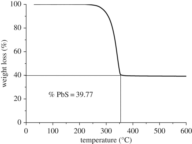
The complex decomposed in a single step to yield a stable residue which is 39.77% of the initial mass of sample used (figure 1). The onset and offset decomposition temperatures were at 216 and 350°C, respectively. The 100% conversion of the complex to PbS results as 44.60% of the total mass. The difference, however, between the two values is 4.90% which implies that the compound can be decomposed to produce PbS as residue [21].
Figure 1.
TGA thermograph of lead diethyldithiocarbamate complex.
Each of the p-XRD patterns of as-deposited PbS thin films was indexed as the face-centred cubic (fcc) phase of PbS (galena) with (111), (200), (220), (311), (222), (400), (311), (420), (422) and (511) as the faces (ICDD 00-003-0614). Generally, there were eight distinct diffraction peaks in the XRD pattern of the PbS obtained at 250, 300 and 400°C. The purity of the PbS produced was highly dependent on the annealing temperature (figure 2). At 200°C, the other peaks in the pattern primarily were as a result of undecomposed precursor which did not match to any phase of PbS. An increase in temperature to 250°C showed the complete decomposition of the precursor to a pure cubic phase PbS with no additional peaks from either the precursor or other phases of PbS. Similar pure PbS phase spectra were obtained at 300 and 400°C confirming the purity of the products [44]. Similar observations on the effect of deposition temperature on the in situ thermal decomposition of lead(II) n-octylxanthate within a 1,3-diisopropenylbenzene–bisphenol A dimethacrylate sulfur copolymer has been reported [45].
Figure 2.
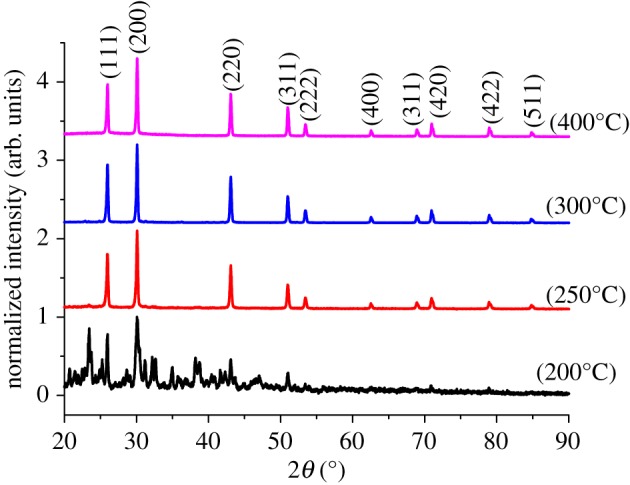
p-XRD pattern of PbS thin films at 200, 250, 300 and 400°C thermal decomposition temperatures.
Structural parameters such as crystallite size (D), dislocation density (δ), lattice constant (a) and strain (ε) were calculated from the p-XRD data [46].
The crystallite size calculated from the Scherrer equation (eqn. (3.1)) ranged from 34.78 to 37.49 nm as the temperature increased from 250 to 400°C (table 1). There was no significant change in the width of the peaks and therefore there was not much significant change in the calculated crystallite sizes.
| 3.1 |
where D is the crystallite size (nanometre), k is a dimensionless shape factor, with a typical value of about 0.9, λ is the wavelength of the radiation, B is the full width at half maximum (FWHM) and θ is the angle of diffraction (Bragg angle).
Table 1.
Structural analyses from p-XRD data.
| temperature (°C) | crystallite size (nm) | size from WH plot (nm) | dislocation density | lattice constant (Ǻ) | strain |
|---|---|---|---|---|---|
| 250 | 34.8 | 50.0 | 0.00082669 | 5.93439 | 0.0010 |
| 300 | 34.9 | 51.28 | 0.00082101 | 5.93375 | 0.0008 |
| 400 | 37.5 | 48.08 | 0.00071149 | 5.93272 | 0.0007 |
There was a decrease in the number of defects, which represents the dislocation density as the crystallite sizes increased (table 1). This may be due to a decrease in the occurrence of grain boundaries as the crystallite size increases with temperature [47,48]. The dislocation density was calculated from Williamson and Smallman's equation,
| 3.2 |
where D is the average crystallite size.
The lattice constant a refers to the physical dimensions of the unit cell in a crystal lattice [21]. Usually, lattices are represented by three constants a, b and c which are referred to as lattice parameters. However, in a special case of a cubic crystal, the three lattices are equal and usually referred to as a. The calculated lattice constant ranged between 5.9327 and 5.9344 Å, which was similar to that of bulk PbS, which is 5.9362 Å [11]. The lattice constant for the cubic phase is determined by using the equation below:
| 3.3 |
where d is the spacing between the planes in the atomic lattice, and h, k and l are the Miller indices.
The Williamson–Hall (WH) plot is a useful tool for graphically demonstrating the hkl-dependence of broadening within a diffraction pattern [49]. A plot of βcosθ/λ against 4sinθ/λ, which is the Williamson–Hall plot, gives a linear plot with strain as the slope and particle size as the inverse of the intercept (electronic supplementary material, figure S1) [50]. The positive slope in the Williamson–Hall plot implies that tensile strain was dominant in all the PbS thin films [51]. The microstrain developed in the film decreases with an increase in annealing temperature. This may be explained as the increase in grain size with an increase in annealing temperature may decrease the surface area of each grain and thereby a reduction in force per unit area between grains and consequently pave the way for strain relaxation [52].
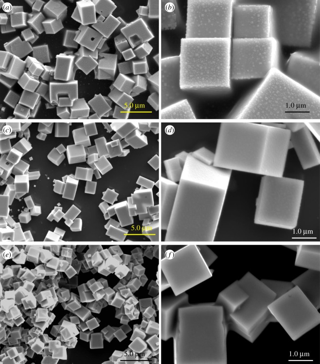
The SEM images of the as-deposited PbS thin films on glass substrate are shown in figure 3. Generally, the overall morphology of the PbS thin films at the three annealing temperatures (250, 300 and 400°C) consist of cubic crystals, with varying degrees of plane-related growth of conjoined interlocking crystals visually evident. The frequency of occurrence of conjoined crystals appeared to vary between the three samples. It was less frequent in the samples at relatively low temperatures (250, 300°C), but very frequent in the sample annealed at high temperature (400°C). The range of crystal dimensions appeared to vary between the annealing temperatures as follows: 1.7–4.4 µm, 1.7–2.3 µm and 1.8–2.0 µm for spin-coated glass substrates annealed at 250, 300 and 400°C, respectively.
Figure 3.
SEM images of all PbS thin films taken at various magnifications (instrument magnifications of 5000× and 20 000×) to illustrate the overall morphology of PbS thin films obtained at 250°C (a,b), 300°C (c,d) and 400°C (e,f).
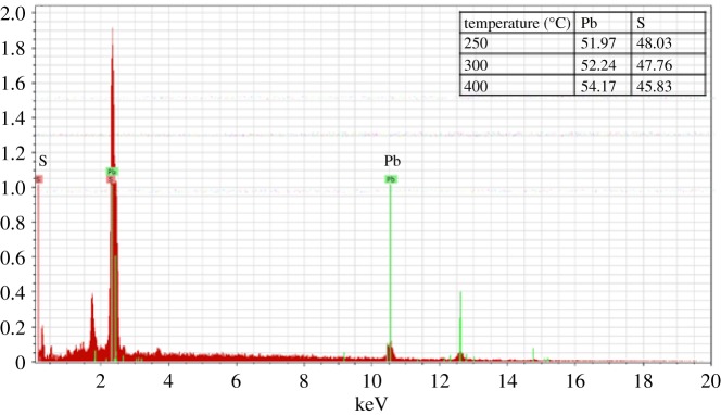
EDX spectroscopy of the PbS thin film did differ significantly from the theoretical ratio of 1 : 1 expected for PbS. Generally, the % S decreased slightly as the annealing temperature was increased from 250 to 400°C (figure 4). However, at all cases, the ratio of Pb to S was approximately 1 : 1 as reported elsewhere in the literature [34].
Figure 4.
EDX spectrum of PbS thin films at 250°C (inset) table of % Pb and % S.
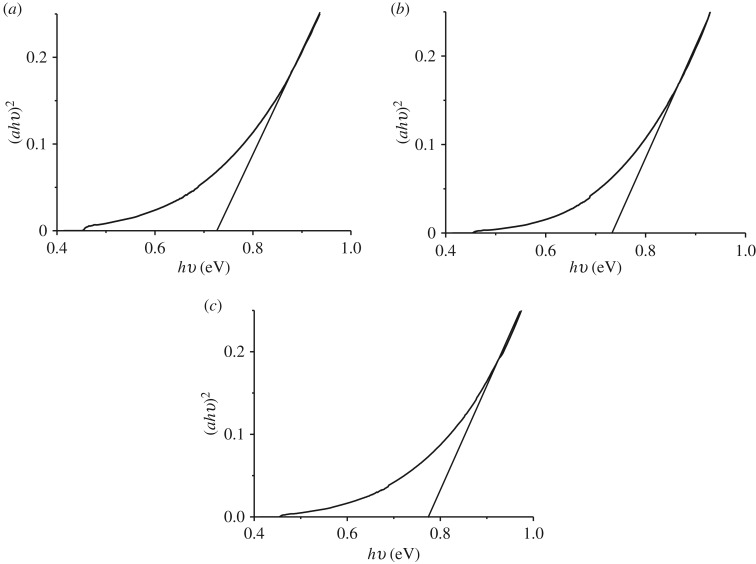
PbS is a direct band gap semiconductor and hence a plot of (αhʋ)2 against hʋ is expected to show a linear portion that corresponds to the energy of the optical band gap when extrapolated to the hʋ axis. Optical properties of PbS were estimated using Tauc plots as 0.72, 0.73 and 0.77 eV for thin films annealed at 250, 300 and 400°C (figure 5). These band gaps were blue shifted from the bulk value of 0.41 eV and also conform to earlier reports on the band gap of PbS thin films as reviewed in the literature [21]. From the band gaps obtained, the PbS thin films can be used as acceptors in solar cells.
Figure 5.
Tauc plots of PbS thin films at (a) 250°C, (b) 300°C and (c) 400°C.
4. Conclusion
Face-centred cubic PbS thin films with the 200 planes as the most preferred orientation have been deposited from lead ethyl carbamate SSP using the spin coating technique followed by annealing at moderate temperatures. SEM analyses revealed the formation of well-resolved cubes of sizes ranging between 1.7 and 2.3 µm depending on the annealing temperature. Optical band gaps of the PbS thin films were estimated to range from 0.72 to 0.77 eV which has been blue shifted from the bulk band gap.
Supplementary Material
Supplementary Material
Acknowledgements
The University of Energy and Natural Resources, Sunyani, Kwame Nkrumah University of Science and Technology, Kumasi and The University of Manchester, United Kingdom are acknowledged for providing laboratory space for this research.
Data accessibility
Data have been uploaded as part of the supplementary material.
Authors' contributions
S.A.S. synthesized and characterized complexes. N.O.B. analysed and wrote the sections of the XRD. D.A.-P. analysed and wrote the sections of the UV–VIS–NIR and band gap. C.W. analysed and wrote the sections of the SEM and EDX.
Competing interests
We declare we have no competing interests
Funding
We received no funding for this study.
References
- 1.Akhtar J, Akhtar M, Malik MA, O'Brien P, Raftery JA. 2012. A single-source precursor route to unusual PbSe nanostructures by a solution–liquid–solid method. J. Am. Chem. Soc. 134, 2485–2487. ( 10.1021/ja209831n) [DOI] [PubMed] [Google Scholar]
- 2.Al-Dulaimi N, Lewis DJ, Zhong XL, Malik MA, O'Brien P. 2016. Chemical vapour deposition of rhenium disulfide and rhenium-doped molybdenum disulfide thin films using single-source precursors. J. Mater. Chem. C 4, 2312–2318. ( 10.1039/C6TC00489J) [DOI] [Google Scholar]
- 3.Buckingham MA, Catherall AL, Hill MS, Johnson AL, Parish JD. 2017. Aerosol-assisted chemical vapor deposition of CdS from xanthate single source precursors. Cryst. Growth Des. 17, 907–912. ( 10.1021/acs.cgd.6b01795) [DOI] [Google Scholar]
- 4.Khan MD, Aamir M, Sohail M, Bhoyate S, Hyatt M, Gupta RK, Sher M, Revaprasadu N. 2019. Electrochemical investigation of uncapped AgBiS2 (schapbachite) synthesized using in situ melts of xanthate precursors. Dalton Trans. 48, 3714–3722. ( 10.1039/C9DT00242A) [DOI] [PubMed] [Google Scholar]
- 5.Tshemese Z, Khan MD, Mlowe S, Revaprasadu N. 2018. Synthesis and characterization of PbS nanoparticles in an ionic liquid using single and dual source precursors. Mater. Sci. Eng. B 227, 116–121. ( 10.1016/j.mseb.2017.10.018) [DOI] [Google Scholar]
- 6.Saah SA, Boadi NO, Wilkins C. 2019. Deposition of PbS thin films from lead hexadecyl and octadecyl xanthate complexes using the spin coating method. MRS Adv. 4, 733–742. ( 10.1557/adv.2019.106) [DOI] [Google Scholar]
- 7.Saah SA, Khan MD, McNaughter PD, Awudza JAM, Revaprasadu N, O'Brien P. 2018. Facile synthesis of a PbS1−xSex (0≤ x≤ 1) solid solution using bis(N, N-diethyl-N′-naphthoylchalcogenoureato)lead(ii) complexes. New J. Chem. 42, 16 602–16 607. ( 10.1039/C8NJ03299H) [DOI] [Google Scholar]
- 8.Boadi NO, Malik MA, O'Brien P, Awudza JAM. 2016. The deposition of PbS and PbSe thin films from lead dichalcogenoimidophosphinates by AACVD. Inorganica Chim. Acta 453, 439–442. ( 10.1016/j.ica.2016.08.023) [DOI] [Google Scholar]
- 9.Malik SN, Akhtar M, Revaprasadu N, Qadeer A, Malik MA. 2014. Dialkyldiselenophosphinato-metal complexes – a new class of single source precursors for deposition of metal selenide thin films and nanoparticles. Mater. Sci. Eng. 64, 1–9. ( 10.1088/1757-899x/64/1/012019) [DOI] [Google Scholar]
- 10.Cant DJH, et al. 2015. Surface properties of nanocrystalline PbS films deposited at the water–oil interface: a study of atmospheric aging. Langmuir 31, 1445–1453. ( 10.1021/la504779h) [DOI] [PubMed] [Google Scholar]
- 11.Boadi NO, Malik MA, O'Brien P, Awudza JAM. 2012. Single source molecular precursor routes to lead chalcogenides. Dalton Trans. 41, 10 497–10 506. ( 10.1039/c2dt30849e) [DOI] [PubMed] [Google Scholar]
- 12.Malik MA, Afzaal M, O'Brien P. 2010. Precursor chemistry for main group elements in semiconducting materials. Chem. Rev. 110, 4417–4446. ( 10.1021/cr900406f) [DOI] [PubMed] [Google Scholar]
- 13.Oellig C, Schwack W. 2017. Comparison of HILIC columns for residue analysis of dithiocarbamate fungicides. J. Liq. Chromatogr. Relat. Technol. 40, 415–418. ( 10.1080/10826076.2017.1315724) [DOI] [Google Scholar]
- 14.Kanemoto-Kataoka Y, Oyama K, Oyama TM, Ishibashi H, Oyama YZ. 2018. Ziram, a dithiocarbamate fungicide, exhibits pseudo-cytoprotective actions against oxidative stress in rat thymocytes: possible environmental risks. Environ. Res. 160, 232–238. ( 10.1016/j.envres.2017.09.027) [DOI] [PubMed] [Google Scholar]
- 15.De Souza LMSD. 2016. Ziram herbicide determination using a polished silver solid amalgam electrode. Electrochim. Acta 224, 541–550. [Google Scholar]
- 16.Kailasa SK, Rohit JV. 2017. Tuning of gold nanoparticles analytical applications with nitro and hydroxy benzylindole-dithiocarbamates for simple and selective detection of terbufos and thiacloprid insecticides in environmental samples. Colloids Surf. A Physicochem. Eng. Asp. 515, 50–61. ( 10.1016/j.colsurfa.2016.11.067) [DOI] [Google Scholar]
- 17.Odularu AT, Ajibade PA. 2019. Dithiocarbamates: challenges, control, and approaches to excellent yield, characterization, and their biological applications. Bioinorg. Chem. Appl. 2019, 1–15. ( 10.1155/2019/8260496.) [DOI] [PMC free article] [PubMed] [Google Scholar]
- 18.Onwudiwe DC, Strydom CA. 2015. The bipyridine adducts of N-phenyldithiocarbamato complexes of Zn(II) and Cd(II); synthesis, spectral, thermal decomposition studies and use as precursors for ZnS and CdS nanoparticles. Spectrochim. Acta A Mol. Biomol. Spectrosc. 135, 1080–1089. ( 10.1016/j.saa.2014.08.004) [DOI] [PubMed] [Google Scholar]
- 19.Trindade T, O'Brien P. 1997. Lead(II) dithiocarbamato complexes as precursors for the LP-MOCVD of lead sulfide. Chem. Vapor Depos. 3, 75–77. ( 10.1002/cvde.19970030203) [DOI] [Google Scholar]
- 20.Lewis EA, et al. 2015. In situ synthesis of PbS nanocrystals in polymer thin films from lead(II) xanthate and dithiocarbamate complexes: evidence for size and morphology control. Chem. Mater. 27, 2127–2136. ( 10.1021/cm504765z) [DOI] [Google Scholar]
- 21.Saah SA, McNaughter PD, Malik MA, Awudza JAM, Revaprasadu N, O'Brien P. 2018. PbSxSe1−x thin films from the thermal decomposition of lead(II) dodecylxanthate and bis(N,N-diethyl-N′-naphthoylselenoureato)lead(II) precursors. J. Mater. Sci. 53, 4283–4293. ( 10.1007/s10853-017-1836-5) [DOI] [Google Scholar]
- 22.Nyamen LD, Pullabhotla VSRR, Nejo AA, Ndifon PT, Warner JH, Revaprasadu N. 2012. Synthesis of anisotropic PbS nanoparticles using heterocyclic dithiocarbamate complexes. Dalton Trans. 41, 8297–8302. ( 10.1039/c2dt30282a) [DOI] [PubMed] [Google Scholar]
- 23.Patel JD, Mighri F, Ajji A, Chaudhuri TK. 2012. Morphology and size control of lead sulphide nanoparticles produced using methanolic lead acetate trihydrate–thiourea complex via different precipitation techniques. Mater. Chem. Phys. 132, 747–755. ( 10.1016/j.matchemphys.2011.12.006) [DOI] [Google Scholar]
- 24.McNaughter PD, Saah SA, Akhtar M, Abdulwahab K, Malik MA, Raftery J, Awudza JAM, O'Brien P. 2016. The effect of alkyl chain length on the structure of lead(ii) xanthates and their decomposition to PbS in melt reactions. Dalton Trans. 45, 16 345–16 353. ( 10.1039/C6DT02859D) [DOI] [PubMed] [Google Scholar]
- 25.Wang N, Cao X, Guo L, Yang S, Wu Z. 2008. Facile synthesis of PbS truncated octahedron crystals with high symmetry and their large-scale assembly into regular patterns by a simple solution route. ACS Nano 2, 184–190. ( 10.1021/nn7000855) [DOI] [PubMed] [Google Scholar]
- 26.Chintso T, Ajibade PA. 2015. Synthesis and structural studies of hexadecylamine capped lead sulfide nanoparticles from dithiocarbamate complexes single source precursors. Mater. Lett. 141, 1–6. ( 10.1016/j.matlet.2014.11.022) [DOI] [Google Scholar]
- 27.Barote MA, Yadav AA, Chavan TV, Masumdar EU. 2011. Characterization and photoelectrochemical properties of chemical bath deposited n-PbS thin films. Dig. J. Nanomater. Biostruct. 6, 979–990. [Google Scholar]
- 28.Li Y-F, Zhang M, Yang Q-J, Zhang F-X, Zheng M-Q, Wang A-J. 2015. A simple and facile solvothermal synthesis of hierarchical PbS microstars with multidendritic arms and their optical properties. J. Nanosci. 2015, 25–27. [Google Scholar]
- 29.Fan D, Thomas PJ, O'Brien P. 2008. Pyramidal lead sulfide crystallites with high energy {113} facets. J. Am. Chem. Soc. 130, 10 892–10 894. ( 10.1021/ja804516q) [DOI] [PubMed] [Google Scholar]
- 30.Wu H, Yang Y, Oh E, Lai F. 2006. Direct synthesis of high-density lead sulfide nanowires on metal thin films towards efficient infrared light conversion. Nanotechnology 23, 265 602–265 609. ( 10.1088/0957-4484/23/26/265602) [DOI] [PubMed] [Google Scholar]
- 31.Ni Y, Wang X, Hong J. 2012. Fast reflux synthesis of multi-armed PbS dendrites, influencing factors and optical properties. RSC Adv. 2, 546–551. ( 10.1039/C1RA00769F) [DOI] [Google Scholar]
- 32.Preetha KC, Remadevi TL. 2015. Effect of hydrazine hydrate concentration on structural, surface morphological and optoelectronic properties of SILAR deposited PbSe thin films. Mater. Sci. Semicond. Process. 39, 178–187. ( 10.1016/j.mssp.2015.04.053) [DOI] [Google Scholar]
- 33.Saravanan RSS, Meena M, Pukazhselvan D, Mahadevan CK. 2015. Structural, optical and electrical characterization of Mn2+ and Cd2+ doped/co-doped PbS nanocrystals. J. Alloys Compd. 627, 69–77. ( 10.1016/j.jallcom.2014.12.008) [DOI] [Google Scholar]
- 34.Veena E, Bangera KV, Shivakumar GK. 2017. Effective role of thickness on structural, electrical and optical properties of lead sulphide thin films for photovoltaic applications. Mater. Sci. Eng. B 223, 64–69. ( 10.1016/j.mseb.2017.06.003) [DOI] [Google Scholar]
- 35.Song C, Sun M, Yin Y, Xiao J, Dong W, Li C, Zhang L. 2016. Synthesis of star-shaped lead sulfide (PbS) nanomaterials and theirs gas-sensing properties. Mater. Res. 19, 1351–1355. ( 10.1590/1980-5373-mr-2015-0683) [DOI] [Google Scholar]
- 36.He J, et al. 2013. Role of sodium doping in lead chalcogenide thermoelectrics. J. Am. Chem. Soc. 135, 4624–4627. ( 10.1021/ja312562d) [DOI] [PubMed] [Google Scholar]
- 37.Xiea BH, Fei GT, Xu SH, Gaoa XD, Zhang JX, Zhang LD. 2018. Tunable broadband wavelength-selective enhancement of responsivity in ordered Au-nanorod array-modified PbS photodetectors. Mater. Chem. C 6, 1767–1773. ( 10.1039/C7TC04884J) [DOI] [Google Scholar]
- 38.Cheng Y, Whitaker MDC, Makkia R, Cocklin S, Whiteside VR, Bumm LA, Roberts KP. 2017. Role of defects and surface states in the carrier transport and nonlinearity of the diode characteristics in PbS/ZnO quantum dot solar cells. Appl. Mater. Interface 9, 13 269–13 277. ( 10.1021/acsami.7b00141) [DOI] [PubMed] [Google Scholar]
- 39.Pitchaimani P, Mun K, Elango KP. 2015. Synthesis, crystal structures, luminescence properties and catalytic application of lanthanide(III) piperidine dithiocarbamate complexes. Polyhedron 93, 8–16. ( 10.1016/j.poly.2015.03.012) [DOI] [Google Scholar]
- 40.Iacovo AD, Venettacci C, Colace L, Scopa L, Foglia S. 2017. High responsivity fire detectors based on PbS colloidal quantum dot photoconductors. IEEE Photonics Technol. Lett. 1135, 1–4. ( 10.1109/lpt.2017.2680741) [DOI] [Google Scholar]
- 41.Tan L, Zhou Y, Ren F, Benetti D, Yang F, Zhao H, Rosei F. 2017. Ultrasmall PbS quantum dots: a facile and greener synthetic route and their high performance in luminescent solar concentrators. J. Mater. Chem. A 5, 10 250–10 260. ( 10.1039/C7TA01372H) [DOI] [Google Scholar]
- 42.Halimehjani AZ, Marjan K, Ashouri A. 2010. Synthesis of dithiocarbamate by Markovnikov addition reaction in aqueous medium. Green Chem. 12, 1306–1310. ( 10.1039/c004711b) [DOI] [Google Scholar]
- 43.Ma X, Hu Y, Zhong H, Wang S, Liu G, Zhao G. 2016. A novel surfactant S-benzoyl-N,N-diethyldithiocarbamate synthesis and its flotation performance to galena. Appl. Surf. Sci. 365, 342–351. ( 10.1016/j.apsusc.2016.01.048) [DOI] [Google Scholar]
- 44.Gottapu S, Muralidharan K. 2016. Room temperature synthesis of organic surfactant-free PbS and PbSe nanoparticles exhibiting NIR absorption. New J. Chem. 40, 832–837. ( 10.1039/C5NJ02794B) [DOI] [Google Scholar]
- 45.McNaughter PD, Bear JC, Mayes AG, Parkin IP, O'Brien P. 2017. The in situ synthesis of PbS nanocrystals from lead(II)n-octylxanthate within a 1,3-diisopropenylbenzene–bisphenol A dimethacrylate sulfur copolymer. R. Soc. open sci. 4, 170 383–170 395. ( 10.1098/rsos.170383) [DOI] [PMC free article] [PubMed] [Google Scholar]
- 46.Popescu V, Rǎducanu D, Dinescu A, Dǎnilǎ M, Popescu GL. 2013. Influence of utltrasounds on structural and morphological properties of PbS deposited on glass substrate. Chalcogenide Lett. 10, 159–165. [Google Scholar]
- 47.Preetha KC, Remadevi TL. 2014. Band gap engineering in PbSe thin films from near-infrared to visible region by photochemical deposition method. J. Mater. Sci. Mater. Electron. 25, 1783–1791. ( 10.1007/s10854-014-1799-0) [DOI] [Google Scholar]
- 48.Rajashree C, Balu AR. 2016. Tuning the physical properties of PbS thin films towards optoelectronic applications through Ni doping. Optik (Stuttg) 127, 8892–8898. ( 10.1016/j.ijleo.2016.06.106) [DOI] [Google Scholar]
- 49.Mozafari M, Moztarzadeh F, Vashaee D, Tayebi L. 2012. Effects of heat treatment on physical, microstructural and optical characteristics of PbS luminescent nanocrystals. Physica E Low Dimens. Syst. Nanostruct. 44, 1429–1435. ( 10.1016/j.physe.2012.03.006) [DOI] [Google Scholar]
- 50.Bhatt SV, Deshpande MP, Soni BH, Garg N, Chaki S. 2013. Chemical bath deposition of lead sulphide (PbS) thin film and their characterization. Solid State Phenom. 209, 111–115. ( 10.4028/www.scientific.net/SSP.209.111) [DOI] [Google Scholar]
- 51.Kumar R, Das R, Gupta M, Ganesan V. 2014. Preparation of nanocrystalline Sb doped PbS thin films and their structural, optical, and electrical characterization. Superlattices Microstruct. 75, 601–612. ( 10.1016/j.spmi.2014.08.019) [DOI] [Google Scholar]
- 52.Remadevi TL, Preetha KC. 2012. Comparative studies on structural, optoelectronic and electrical properties of SILAR grown PbS thin films from acidic, neutral and alkaline cationic reaction bath. J. Mater. Sci. Mater. Electron. 23, 2017–2023. ( 10.1007/s10854-012-0696-7) [DOI] [Google Scholar]
Associated Data
This section collects any data citations, data availability statements, or supplementary materials included in this article.
Supplementary Materials
Data Availability Statement
Data have been uploaded as part of the supplementary material.


