Abstract
We demonstrate the fabrication of micropore and nanopore features in hollow antiresonant reflecting optical waveguides to create an electrical and optical analysis platform that can size select and detect a single nanoparticle. Micropores (4 μm diameter) are reactive-ion etched through the top SiO2 and SiN layers of the waveguides, leaving a thin SiN membrane above the hollow core. Nanopores are formed in the SiN membranes using a focused ion-beam etch process that provides control over the pore size. Openings as small as 20 nm in diameter are created. Optical loss measurements indicate that micropores did not significantly alter the loss along the waveguide.
Subject terms: micropore, nanopore, antiresonant reflecting optical waveguide, microfluidic channels, focused ion beam, optical loss
1 Introduction
This paper concentrates on the fabrication and integration of nanometer-sized openings (nanopores) in hollow antiresonant reflecting optical waveguide (ARROW)-based fluorescence platforms with solid-core waveguides and fluid reservoirs.1,2 These ARROW-based structures were previously demonstrated,3,4 but the inclusion of a nanopore into an ARROW represents a significant advancement in optofluidic integration targeted at single particle analysis. Biological and solid state nanopores have been fabricated using various techniques and successfully used to measure single particle signatures in electrical current blockade tests.5 For example, biological nanopores that spontaneously insert themselves in lipid membranes have been created using the α-hemolysin protein. Kasianowicz et al. showed that an electric field biased at 100 mV providing a continuous current of ~100 pA can drive single stranded RNA and DNA molecules through a 2.2-nm-diam α-hemolysin ion channel in a lipid membrane.6 Nanopores fabricated from solid state materials have been shown to be more mechanically and chemically stable and their sizes can be adjusted for specific applications. Heng et al. made solid state 1.2-nm-diam nanopores by sputtering a 30-nm-thick Si3N4 membrane using a high-energy focused electron beam, however, low etch rates limit the thickness of the membrane for this method.7 By applying an unfocused ion beam, Li et al.8 were able to reduce the diameter of a 100- to 150-nm nanopore sputtered in a Si3N4 membrane with a high-energy Ar+ beam to 5 nm. The membrane separated two compartments biased at 120 mV with a constant ionic current of 1.66 nA through the nanopore that they used to measure the diffusion of double-stranded DNA. Additionally, Storm et al.9 also used a high-energy electron beam to reduce the diameter of a 20-nm nanopore etched in a 10-nm-thick SiO2 membrane to 2 nm. Allen et al. formed 50- to 200-nm nanopores in SiN membranes by focused ion-beam drilling in combination with ion-beam-assisted thin film deposition.10 Siwy and Fulinski used electrochemical etching to create conical nanopores with diameters as small as 2 nm at the aperture of the cone tip in circular polyethylene terephthalate (PET) foils.11 Particle detection and analysis in each of these cases was done electrically by measuring ionic current changes as a particle passed through the nanopore. The motivation for combining nanopores with ARROW platforms is the ability to correlate electrical current blockade and optical fluorescence signals providing sensitive nanoparticle detection.
Optical fluorescence is another primary method used to analyze small numbers of single particles.12 Fluorescence is used to study molecular phenomena and interactions such as DNA structural rearrangements,13,14 ribosome kinetics,15 and protein conformational dynamics.16–18 Some examples of conventional fluorescence detection and analysis techniques include epifluorescence,12 confocal microscopy,12 evanescent field sensors,19 and fluorescence correlation spectroscopy.20,21 However, typical analysis schemes are based on bulky microscopy instruments, therefore, an integrated ARROW fluorescence platform that uses planar waveguides for analysis is an attractive approach to reduce cost, time, analyte volumes, and device size (~1 cm2). However, to use the ARROW to perform fluorescence analysis it is important that the fabrication techniques for the integration of the nanopore do not significantly alter the optical properties and structural integrity of the waveguide.
2 Micropore/Nanopore Integrated Analysis Platform
The ARROW analysis platform is made up of alternating dielectric layers that act as Fabry-Pérot reflectors in the direction transverse to the propagation of light. When operating at antiresonance, the layers have a high reflectivity that enables light to be guided in the core of the hollow ARROW waveguide.22 The condition for antiresonance is satisfied by growing the dielectric layers to specific thicknesses given by
| (1) |
where tj is the thickness of the j’th layer; nj and nc are the indices of refraction of the j’th layer and the core, respectively; dc is the thickness of the core; λ is the wavelength; and N is an integer representing the antiresonance order. An example of a side view of an ARROW waveguide is shown in Fig. 1. We use plasma-enhanced chemical vapor deposition (PECVD) SiN and SiO2 as our dielectric layers at thicknesses of toxide=270 nm and tnitride=93 nm when nnitride=2.05, noxide=1.47, nc =1.33, dc =5 μm, N =0, and λ = 633 nm, though this structure exhibits low propagation loss over a broad wavelength range from 500 to 700 nm. In addition, we deposited a SiO2 layer that is 4 μm thick over our top ARROW layers that we used to etch solid core waveguides in and provide structural support.
Fig. 1.
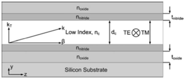
Side view of an ARROW waveguide.
Figure 2 illustrates the functionality of a micropore and nanopore integrated with a hollow ARROW analysis platform. The integration with nanopores poses a unique challenge in integrated optics because ARROWs are constructed of dielectric layers that are a total of several micrometers thick and have a nonflat geometry. This makes it difficult to controllably mill nanopores with diameters of 25 to 100 nm through a complete dielectric stack. To provide a thinner starting layer, a micrometer-sized pore (micropore) was first etched into the ARROW. The micropore exposed a thin SiN layer directly above the hollow core of the ARROW that a nanopore was milled into. A zoomed in view of the micropore, nanopore, and the thin SiN layer are shown in Fig. 2(a). The hollow-core ARROW, the intersecting solid-core waveguides at the ends and middle of the hollow-core ARROW, and the location of the micropore and nanopore are shown in Fig. 2(b). The geometry of the hollow-core and solid-core waveguides was used in earlier experiments.3 Fluorescence detection takes place when fluorophores are excited by the solid-core waveguides intersecting the hollow-core waveguide. Placing a micropore/nanopore feature directly above the hollow-core ARROW will allow for control of particles entering the detection region.
Fig. 2.
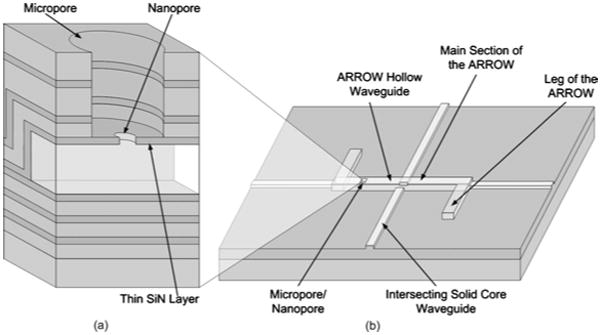
Cross section of a micropore/nanopore integrated with the ARROW hollow core waveguide lab-on-a-chip platform.
3 Micropore and ARROW Fabrication
Figure 3 shows how fabrication of the micropore fits within our established ARROW fabrication process.3,23 Figure 3(a) shows the deposition of a 2-μm layer of thermal oxide that provides isolation from the silicon wafer. Alternating layers of SiO2 and SiN that form the bottom part of the hollow waveguide were deposited using PECVD at thicknesses dictated by the ARROW guiding condition,3,24 are also shown in Fig. 3(a). The PECVD SiN was grown with a mixture of 5% silane in helium (SiH4/He) and ammonia (NH3), at 250 °C, 70 W of rf power, and 1 Torr. The PECVD SiO2 was grown with a mixture of 5% silane in helium (SiH4/He) and nitrous oxide (N2O), at 250 °C, 23 W, and 600 mTorr. A patterned and reflowed rectangular SU8-3005 (Ref. 3) photoresist core is shown in Fig. 3(b). The SU8 photoresist core was used as a sacrificial material that was removed in later processing steps that formed the hollow part of the waveguide. Figure 3(c) shows the first SiN ARROW layer that was deposited over the SU8-3005 core. Nanopore features were milled into this SiN layer in later processing steps.
Fig. 3.
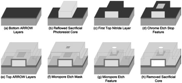
Fabrication flow diagram of the process of creating a micropore in a hollow ARROW waveguide.
The deposition and patterning of a chrome square etch stop feature is shown in Fig. 3(d). The etch stop feature is an 8×8-μm2, 200-nm-thick chrome square that was fabricated using a liftoff technique. The chrome etch stop feature keeps the SiN layer below it intact during a subsequent reactive-ion etching (RIE) that forms the micropore.
Figure 3(e) shows the remaining ARROW SiO2 and SiN layers that were deposited to form the top and sides of the hollow waveguide. The introduction of the chrome etch stop feature does not change the process requirements for the remaining ARROW layers. The total thickness of these layers is 5 μm. The micropore etch mask that was patterned and aligned directly over the chrome etch stop feature is shown in Fig. 3(f). This was accomplished by patterning a 4×4-μm2 SU8-3005 square directly on top of the hollow waveguide. A 200-nm layer of chrome was deposited over the SU8-3005 squares and then the wafer was placed in acid that lifted off the chrome over the SU8-3005 squares. Figure 3(g) shows the ARROW hollow waveguides after the micropore etch was completed and the micropore etch mask was removed. The chrome etch stop feature at the bottom of the micropore was removed using a wet chrome etchant, leaving the underlying SiN membrane exposed.
Finally, Fig. 3(h) shows the ARROW after the rectangular SU8-3005 photoresist core was removed in a piranha solution [(1:1) (H2O2:H2SO4)] at 130 °C, forming the waveguide’s hollow core, which can be subsequently filled with liquids and test particles.
4 Micropore Etching Process
Etching a micropore into the top layers of an ARROW allowed us access to the SiN layer over the core where a nanopore could be milled. The most important consideration during the micropore etch was keeping the relatively thin SiN layer intact. We determined that depositing an etch stop layer over the SiN layer was a more reliable and higher yield approach to cover and protect the SiN layer than using a timed RIE etch process.
While the fabrication of this etch stop feature was straightforward, we had to select a material that was not sputtered away during the micropore RIE etch process. The micropore RIE etch process was performed using an Anelva RIE DEM-451, 13.56-MHz system employing tetrafluoromethane CF4. The CF4 gas was chosen primarily for its high selectivity etching of SiO2 and SiN films.
Six different materials were investigated as possible etch stop candidates: chrome, titanium, aluminum, nickel, positive photoresist AZ3330, and negative photoresist SU8-3005. Our selection criteria were based on the materials RIE etch rate selectivity. Table 1 shows that titanium and chrome both have very low etch rates under the conditions used for etching through SiO2 and SiN layers. While specific etch rates will vary for different RIE machines and etch conditions, we expected the general trends to hold for fluorine-based etches. Chrome was chosen for the production of micropores because it had a highest RIE etch selectivity and it was straightforward to pattern and remove in a commercially available wet etchant.
Table 1.
Average RIE etch rate (in nanometers per minute) for a set of possible etch stop materials.
| Material | Average Etch Rate (nm/min) |
|---|---|
| SiO2 | 111 |
| AZ3330 | 107 |
| SU8-3005 | 255 |
| Aluminum | 3.65 |
| Nickel | 1.48 |
| Titanium | 0.97 |
| Chrome | 0.60 |
The recipe used is a CF4 etch gas at a flow rate of 25 standard cubic centimeters per minute (SCCM), rf power of 300 W, and a chamber pressure of 100 mTorr.
Figure 4 shows two scanning electron microscope (SEM) images of micropores etched into ARROWs. A zoomed out view that also shows the intersection of a solid-core waveguide with a hollow-core waveguide is shown in Fig. 4(a). The smooth [5-nm root mean square (rms) measured by a Vecco Dimension 3100 atomic force microscope with a 1-×1-μm scanning region] flat SiN membrane surface at the bottom of the micropore is shown in Fig. 4(b).
Fig. 4.
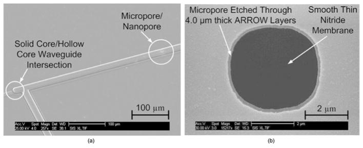
(a) SEM of an intersection of a hollow and solid core waveguide and a micropore on the ARROW hollow waveguide and (b) SEM image of the top view close-up of micropore.
5 Nanopore Formation
To demonstrate the ability to combine the micropore fabrication process with the addition of nanopores, we milled a nanopore in the thin SiN membrane at the bottom of the etched micropore using a focused-ion-beam (FIB) etching process.25,26 We used a dual-beam FEI Strata DB 235 FIB that had a 30-kV accelerating voltage for liquid Ga+ ions and current apertures ranging from 1 pA to 20 nA. The formation of nanopores that had diameters between 20 and 100 nm is shown in Fig. 5. Initially, the diameter of the nanopore was 100 nm. While this size was generally adequate for the detection of particles that had the dimensions of large viruses (100 to 150 nm), subsequently shrinking the nanopore to smaller sizes (20 to 40 nm) would enable us to sense and size select smaller biomolecules. The shrinking process of the nanopore is based on the irradiation of the SiN layer area (about 1 μm2) around the nanopore with Ga+ ions in the FIB scanning mode.25,26 Two main theoretical models are believed to be responsible for the shrinking of the nanopore. The first is the viscous flow model where an impinging Ga+ ion breaks the bonds in the SiN layer and allows for the flow of material. With the SiN layer in this fluidized state, the nanopore will deform to find a configuration with a lower surface free energy. If the diameter of the initial nanopore is less than the thickness of the SiN layer, then the nanopore can lower its surface free energy by shrinking its diameter.9 The second theory that explains the shrinking of the nanopore is the surface adatom diffusion model. This model is based on the theory that impinging Ga+ ions generate surface adatoms, which move about the surface of the SiN layer by diffusion. The shrinking of the nanopore happens when the adatoms diffuse into the nanopore and bind on its edge.27 The initial size of our FIB milled nanopore was 100 nm. After a series of FIB scans, the diameter of the nanopore was controllably decreased to 20 nm.
Fig. 5.

SEMs showing the size of the nanopore being reduced from 100 to 20 nm after a series of FIB scans. The smallest dimension is reported as a characteristic size of the nanopore.
6 Optical Loss Measurement and Characterization
An important question was whether the micropore and nanopore features would lead to deterioration in the optical guiding properties if it was placed in the collection section of the ARROW hollow-core waveguide. Theoretically the size of the nanopore/micropore is small enough (4 × 4 μm) that any additional optical losses it introduces in the modified layer structure of the ARROW will not have a significant effect on the total optical throughput. For example, even if the micropore/nanopore had introduced a high loss of 100 cm−1, only 4% of the optical power would be lost because of the small dimensions of the micropore (4×4 μm) and nanopore (20 nm diameter) site. While low loss in the section of the ARROW with the micropore/nanopore site was confirmed with a commercial mode solver program (Photon Design), losses in realized devices can differ, for example, by design layer thickness deviations, transitions from multiple to single layers, and wall roughness. The optical loss was measured by observing optically induced motion of dielectric particles (1 μm diameter, n ~ 1.59, Duke Scientific) in the hollow core waveguide.28 The test configuration for the loss measurements is shown in Fig. 6(a). A particle in the reservoir entered the ARROW hollow-core waveguide where an Nd:YAG laser (power ≈ 12 mW) optically induced motion of the particle. The particle was optically pushed down the length of the waveguide and passed the micropore/nanopore site. The particle location was observed perpendicular to the chip plane through a microscope [0.5 numerical aperture (NA), 50×] and a tracking program was utilized for analysis. Figure 6(b) shows the experimentally observed trajectory (circles) of a particle in an ARROW that had a micropore/nanopore site, the calculated particle trajectory that did not have a micropore/nanopore site (solid line), and the calculated particle trajectory that had a micropore site with a loss of 100 cm−1 (dashed line). As we can see, the trajectory without a micropore site (solid line) is not measurably different, within experimental error, from the trajectory with a site of 100 cm−1 loss (dashed line). Additionally, the observed trajectory closely resembles the calculated trajectory without a nanopore site. Therefore, the results indicate the additional loss introduced by the micropore/nanopore is not significant.
Fig. 6.
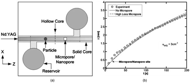
(a) Setup used to perform the particle pushing experiment to measure optical loss and (b) axial particle position versus time for an experimentally observed particle trajectory (circles) in an ARROW with a micropore/nanopore site, the calculated trajectory in an ARROW without a micropore/nanopore site (solid line), and the calculated trajectory in an ARROW with a micropore/nanopore site loss of 100 cm−1 loss (dashed line).
7 Conclusion
Small, simple, cheap, and fast sensors to detect single nanoparticles are desirable. We demonstrated a fabrication technique that can be applied to these types of sensors by combining synthetic nanopores and hollow ARROW waveguides. A hybrid micropore/nanopore fabrication process was developed to define nanopores in ARROW waveguides that have walls that are several micrometers thick. A chrome etch stop feature keeps the thin SiN membrane, where the nanopore is drilled, intact during micropore etching. We demonstrated that nanopores of variable size down to 20 nm can be drilled in the SiN membrane using an FIB process. Optical measurements show that the addition of micropores and nanopores does not measurably alter the transmission of the ARROW waveguide. In the future, the integrated ARROW platform and nanopore can be used to combine and correlate electrical current blockade data and fluorescently detected signal with single nanoparticle resolution.
Acknowledgments
We gratefully acknowledge stimulating discussions with D. W. Deamer and financial support from the National Institutes of Health/National Institute of Biomedical Imaging and Bioengineering (NIH/NIBIB) (Grant No. R01-EB006097), the National Science Foundation (NSF) (Grants ECS-0528714 and ECS-0528730), the W. M. Keck Center for Nanoscale Optofluidics at University of California at Santa Cruz, and the Materials Research Laboratory at the University of California at Santa Barbara.
Footnotes
Biographies and photographs of the authors not available.
Contributor Information
Matthew R. Holmes, Brigham Young University, Electrical and Computer Engineering Department, 459 Clyde Building, Provo, Utah 84602
Tao Shang, Brigham Young University, Electrical and Computer Engineering Department, 459 Clyde Building, Provo, Utah 84602.
Aaron R. Hawkins, Email: hawkins@ee.byu.edu, Brigham Young University, Electrical and Computer Engineering Department, 459 Clyde Building, Provo, Utah 84602
Mikhail Rudenko, University of California Santa Cruz, School of Engineering, 1156 High Street, Santa Cruz, California 95064.
Philip Measor, University of California Santa Cruz, School of Engineering, 1156 High Street, Santa Cruz, California 95064.
Holger Schmidt, University of California Santa Cruz, School of Engineering, 1156 High Street, Santa Cruz, California 95064.
References
- 1.Yin D, Lunt EJ, Barman A, Hawkins AR, Schmidt H. Microphotonic control of single molecule fluorescence correlation spectroscopy using planar optofluidics. Opt Express. 2007;15:7290–7295. doi: 10.1364/oe.15.007290. [DOI] [PubMed] [Google Scholar]
- 2.Yin D, Barber JP, Deamer DW, Hawkins AR, Schmidt H. Single-molecule detection using planar integrated optics on a chip. Opt Lett. 2006;31:2136–2138. doi: 10.1364/ol.31.002136. [DOI] [PubMed] [Google Scholar]
- 3.Yin D, Schmidt Holger, Barber J, Hawkins A. Integrated ARROW waveguides with hollow cores. Opt Express. 2004;12:2710–2715. doi: 10.1364/opex.12.002710. [DOI] [PubMed] [Google Scholar]
- 4.Yin D, Lunt EJ, Rudenko MI, Deamer DW, Hawkins AR, Schmidt H. Planar optofluidic chip for single particle detection, manipulation, and analysis. Lab Chip. 2007;7:1171–1175. doi: 10.1039/b708861b. [DOI] [PubMed] [Google Scholar]
- 5.Dekker C. Solid-state nanopores. Nat Nanotechnol. 2007;2:209–215. doi: 10.1038/nnano.2007.27. [DOI] [PubMed] [Google Scholar]
- 6.Kasianowicz J, Brandin E, Branton D, Deamer D. Characterization of individual polynucleotide molecule using a membrane channel. Proc Natl Acad Sci USA. 1996;93:13770–13773. doi: 10.1073/pnas.93.24.13770. [DOI] [PMC free article] [PubMed] [Google Scholar]
- 7.Heng JB, Ho C, Kim T, Timp R, Aksimentiev A, Grinkova YV, Sligar S, Schulten K, Timp G. Sizing DNA using a nanometer-diameter pore. Biophys J. 2004;87:2905–2911. doi: 10.1529/biophysj.104.041814. [DOI] [PMC free article] [PubMed] [Google Scholar]
- 8.Li J, Stein D, McMullan C, Branton D, Aziz MJ, Golovchenko JA. Ion-beam sculpting at nanometre length scales. Nature. 2001;412:166–169. doi: 10.1038/35084037. [DOI] [PubMed] [Google Scholar]
- 9.Storm AJ, Chen JH, Ling XS, Zandbergen HW, Dekker C. Fabrication of solid-state nanopores with single-nanometre precision. Nature Mater. 2003;2:537–540. doi: 10.1038/nmat941. [DOI] [PubMed] [Google Scholar]
- 10.Allen FI, Persaud A, Park SJ, Minor A, Sakurai M, Schneide DH, Schenkel T. Transport of multiply and highly charged ions through nanoscale apertures in silicon nitride membranes. Nucl Instrum Methods Phys Res B. 2006;244:323–326. [Google Scholar]
- 11.Siwy Z, Fulinski A. Fabrication of a synthetic nanopore ion pump. Phys Rev Lett. 2002;89:198103. doi: 10.1103/PhysRevLett.89.198103. [DOI] [PubMed] [Google Scholar]
- 12.Moener WE, Fromm DP. Methods of single-molecule fluorescence spectroscopy and microscopy. Rev Sci Instrum. 2003;74:3597–3619. [Google Scholar]
- 13.Grunwell JR, Glass JL, Lacoste TD, Deniz AA, Chemla DS, Schultz P. Monitoring the conformational fluctuations of DNA hairpins using single-pair fluorescence resonance energy transfer. J Am Chem Soc. 2001;123:4295–4303. doi: 10.1021/ja0027620. [DOI] [PubMed] [Google Scholar]
- 14.McKinney SA, Declais AC, Lilley DMJ, Ha T. Structural dynamics of individual holliday junctions. Nat Struct Biol. 2003;10:93–97. doi: 10.1038/nsb883. [DOI] [PubMed] [Google Scholar]
- 15.Zhuang X, Bartley LE, Babcock HP, Russell R, Ha T, Herschlag D, Chu S. A single-molecule study of RNA catalysis and folding. Science. 2000;288:2048–2051. doi: 10.1126/science.288.5473.2048. [DOI] [PubMed] [Google Scholar]
- 16.Ha T, Ting AY, Liang J, Caldwell WB, Deniz AA, Chemla DS, Schultz PG, Weiss S. Single molecule fluorescence spectroscopy of enzyme conformational dynamics and cleavage mechanism. Proc Natl Acad Sci USA. 1999;96:893–898. doi: 10.1073/pnas.96.3.893. [DOI] [PMC free article] [PubMed] [Google Scholar]
- 17.Rhoades E, Gussakovsky E, Haran G. Watching proteins fold one molecule at a time. Proc Natl Acad Sci USA. 2003;100:3197–3202. doi: 10.1073/pnas.2628068100. [DOI] [PMC free article] [PubMed] [Google Scholar]
- 18.Talaga DS, Lau WL, Roder H, Tang J, Jia Y, DeGrado WF, Hochstrasser RM. Dynamics and folding of single two-stranded coiled-coil peptides studied by fluorescent energy transfer confocal microscopy. Proc Natl Acad Sci USA. 2000;97:13021–13026. doi: 10.1073/pnas.97.24.13021. [DOI] [PMC free article] [PubMed] [Google Scholar]
- 19.Taitt CR, Anderson GP, Ligler FS. Evanescent wave fluorescence biosensors. Biosens Bioelectron. 2005;20:2470–2487. doi: 10.1016/j.bios.2004.10.026. [DOI] [PubMed] [Google Scholar]
- 20.Medina M, Schwille P. Fluorescence correlation spectroscopy for the detection and study of single molecules in biology. BioEssays. 2002;24:758–764. doi: 10.1002/bies.10118. [DOI] [PubMed] [Google Scholar]
- 21.Rudenko M, Kühn S, Lunt E, Deamer D, Hawkins A, Schmidt H. Ultrasensitive Qβ phase analysis using fluorescence correlation spectroscopy on an optofluidic chip. Biosens Bioelectron. 2009;24:3258–3263. doi: 10.1016/j.bios.2009.04.005. [DOI] [PMC free article] [PubMed] [Google Scholar]
- 22.Schmidt H, Hawkins AR. Optofluidic waveguides: I. Concepts and implementations. Microfluid Nanofluid. 2008;4:3–16. doi: 10.1007/s10404-007-0199-7. [DOI] [PMC free article] [PubMed] [Google Scholar]
- 23.Hawkins AR, Schmidt H. Optofluidic waveguides: II. Fabrication and structures. Microfluid Nanofluid. 2008;4:17–32. doi: 10.1007/s10404-007-0194-z. [DOI] [PMC free article] [PubMed] [Google Scholar]
- 24.Dugay MA, Kokubun Y, Koch TL, Pfeiffer L. Antiresonant reflecting optical waveguides in SiO2–Si multilayer structures. Appl Phys Lett. 1986;49:13. [Google Scholar]
- 25.Rudenko MI, Yin D, Holmes M, Hawkins AR, Schmidt H. Integration and characterization of SiN nanopores for single-molecule detection in liquid-core ARROW waveguides. Ultrasensitive and Single-Molecule Detection Technologies II, Proc SPIE. 2007;6444:64440L. [Google Scholar]
- 26.Lo CJ, Aref T, Bezryadin A. Fabrication of symmetric sub-5 nm nanopores using focused ion and electron beams. Nanotechnology. 2006;17:3264–3267. [Google Scholar]
- 27.Cai Q, Ledden B, Krueger E, Golvchenko JA, Li J. Nanopore sculpting with noble gas ions. J Appl Phys. 2006;100:024914. doi: 10.1063/1.2216880. [DOI] [PMC free article] [PubMed] [Google Scholar]
- 28.Measor P, Kühn S, Lunt EJ, Phillips BS, Hawkins AR, Schmidt H. Hollowcore waveguide characterization by optically induced particle transport. Opt Lett. 2008;33:672–674. doi: 10.1364/ol.33.000672. [DOI] [PMC free article] [PubMed] [Google Scholar]


