Abstract
We report a simple and scalable technique for the fabrication of nanopore arrays on freestanding SiN and graphene membranes based on electron-beam lithography and reactive ion etching. By controlling the dose of the single-shot electron-beam exposure, circular nanopores of any size down to 16 nm in diameter can be fabricated in both materials at high accuracy and precision. We demonstrate the sensing capabilities of these nanopores by translocating dsDNA through pores fabricated using this method, and find signal-to-noise characteristics on par with TEM-drilled nanopores. This versatile lithography-based approach allows for the high-throughput manufacturing of nanopores and can in principle be used on any substrate, in particular membranes made out of transferable 2D materials.
Keywords: nanopore array, reactive ion etching, 2D materials, graphene nanopore, electron beam lithography
Introduction
Solid-state nanopores drilled in a thin membrane are unique tools that allow for label-free high-throughput single-molecule investigation of biomolecules such as DNA, proteins, and peptides chains1. Their robustness, versatility, and ease of integration in CMOS processing are paramount to the sustained interest this class of biosensors has received over the past 15 years2. The principle of interrogation for nanopore sensing derives elegance from its simplicity: a nanopore, typically drilled in a 20 nm thick membrane, defines a nanoscale sensing volume through which biomolecules can be probed on passage, usually via an ionic-current readout3. More recently, nanopores in single-layer materials like graphene and MoS2 have received a great deal of attention, as the two-dimensional (2D) nature of these materials drastically reduces the sensing volume and helps to enhance the signal4, 5. Both SiN and 2D nanopores have been used to provide insight into many complex biophysical phenomena, such as DNA-protein interactions4-8, protein-protein interactions9, 10, and DNA polymer physics11-13. However nanopore fabrication is typically slow and expensive, particularly in 2D materials, preventing large-scale use of solid-state nanopores in commercial applications, such as clinical sensors for the detection of biomolecules in diagnostics9.
Currently, there are several techniques for the production of nanopores. First and foremost is the use of the electron beam of a Transmission Electron Microscope (TEM)14-16. This technique provides sub-nanometer precise control over the pore's diameter, but is very low in throughput, especially for larger sized nanopores (>15 nm)17, very expensive, and labor intensive. Furthermore, nanopores are notoriously hard to fabricate in 2D materials with conventional TEM drilling due to their sensitivity to carbon deposition and membrane damage18. Hence, the method lacks scalability and cost efficiency which are both required for commercialization. Fabrication using Helium Ion Microscope (HIM) is a promising, more high-throughput alternative for the fabrication of nanopores, but also requires access to expensive and delicate instrumentation19, 20. An alternative cost-effective technique is nanopore fabrication by controlled dielectric breakdown, where a nanopore is created by the timed termination of a large transmembrane voltage stress (∼10V)21,22. However, the stochastic nature of the breakdown process does not provide control over the position of the nanopore23. Other techniques use ion bombardment and subsequent chemical24, 25 or electrochemical wet etching26. Whereas these techniques can be used at high throughput, challenges remain in the timed termination of the wet etching17 and the associated uniformity of the pore size.
Chemical dry etching or reactive ion etching (RIE) is a more promising alternative for high-throughput fabrication of large nanopores. In this widely used technique a pattern is predefined in a resist by electron-beam lithography (EBL), which is the standard technique used to define high-resolution structure in microfabrication, and is transferred into a substrate by plasma etching using reactive ions27. The directionality of the RIE process preserves the resolution obtained in the EBL pattern and allows for the resolution to be defined on a wafer scale27-30. The chemical dry etching allows a range of substrates to be used as membrane material28, notably including 2D materials that require a transfer step. To exploit the potential of this technique for transferable materials, the EBL patterning should be performed on a freestanding membrane. Furthermore, patterning on a thin membrane can improve resolution, because it eliminates electron backscatter 31.
Here, we present a novel and simple method for rapid nanopore fabrication based on electron-beam lithography with reactive ion etching. By patterning the nanopores as a last step in the fabrication process, in principle any (transferable) membrane material can be readily used. To demonstrate the flexibility of this technique, we create single nanopores and nanopore arrays in both 20 nm thick SiN and single-layer graphene membranes. TEM inspection shows that the fabricated nanopores are highly circular and uniform in size. We show that the nanopore diameter can be set with nanometer precision by controlling the electron-beam dose. Finally, we demonstrate lambda-DNA translocations through nanopores fabricated using this method. Although applied here for single-molecule biosensing, we anticipate that this simple, high-throughput, and versatile nanopore fabrication technique will find applications in other domains of the nanopore research field such as filtration, power generation and chemical sensing 2, 4, 32, 33.
Results and discussion
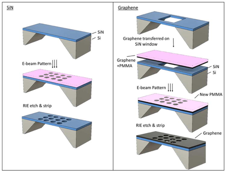
Figure 1A outlines a schematic of the fabrication protocol for the production of a nanopore array in SiN. First, a layer a 100 nm thick layer of poly(methyl methacrylate) (PMMA-A3, 495K) electron sensitive resist (MicroChem Corp) is spin-coated on top of the chip containing a freestanding SiN membrane. Details about the fabrication of the support can be found in the Supporting Information (SI). Subsequently, the layer is patterned by exposing the resist with a 100 keV electron bundle from the electron-beam pattern generator (EBPG5200, Raith), using one single shot of e-beam exposure per nanopore. After exposure, the PMMA is developed in a 1:3 mixture of methyl isobutyl ketone (MIBK) and isopropyl alcohol (IPA) for 1 min. Finally, the pattern is transferred into the SiN membrane by reactive ion etching with CHF3 (100 sec, 50 W, 50 sccm of CHF3, 2.5 sccm of O2, 8.6 μbar, Leybold) and the resist is stripped in hot acetone (50°C) for 2 hours.
Figure 1. Schematic of EBL assisted RIE nanopore fabrication.

A) Fabrication process on SiN membrane. A 100 nm thick layer of PMMA is spin-coated on a SiN membrane prior to e-beam patterning. The pattern is transferred into the SiN membrane by reactive ion etching in a CHF3 plasma. Finally, the remaining resist is stripped in hot acetone (50°C) leaving a functional nanopore array. B) The same process on the graphene membrane. A graphene layer with a supporting PMMA layer is deposited on a pre-etched SiN window. The supporting layer of PMMA is stripped and a new 150 nm of PMMA is deposited prior to e-beam patterning. The pattern is transferred into the graphene membrane by reactive ion etching in an oxygen plasma. Finally, the remaining resist is stripped in m-xylene, leaving a functional nanopore array.
The fabrication of the graphene nanopore array (Fig. 1B) is analogous to the fabrication of the SiN nanopores. First, a layer of graphene (Graphenea, single layer CVD graphene on copper) is transferred onto a SiN membrane pre-patterned with square windows 1 μm in size, creating 1×1 μm freestanding areas of graphene (see SI). Then, a 150 nm thick layer of PMMA is spin-coated on top of the chip and the resist is exposed by a single shot from the electron beam. We note that thicker PMMA is used in the graphene nanopore arrays because the graphene requires an oxygen etch which also etches the PMMA mask substantially. After the development of the resist in 1:3 MIBK:IPA for one minute, the pattern is transferred into the graphene layer by reactive ion etching with oxygen (20 sec, 50 W, 20 sccm of O2, 3.3 μbar, Leybold). The remaining resist is stripped for 20 min in hot m-xylene (85°C) and air-dried. To avoid collapsing the freestanding graphene layer, the sample is gently plunged vertically into the solution. After 20 mins, the sample is removed and placed at an angle (∼20 degrees to the horizontal plane) to allow the remaining droplet of m-xylene to evaporate.
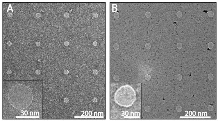
Figure 2 shows example TEM images of nanopore arrays fabricated in both SiN (Fig. 2A) and in freestanding graphene (Fig. 2B) using the protocol outlined above. The nanopores in these examples were 29 ± 3 nm and 38 ± 2 nm (average ± standard deviation) in diameter, for the SiN and graphene respectively. The nanopores produced are highly circular; The average ratio between their major and minor axis (major/minor) is 1.08±0.08 for the SiN arrays and 1.08±0.14 for the graphene nanopore arrays. We note that the graphene pores fabricated through this method seem to exhibit much less carbon deposition around the edges of the pore than conventionally drilled TEM graphene pores 34.
Figure 2. TEM image of nanopore arrays fabricated using RIE.

A) Nanopore array fabricated in a SiN membrane. The array was fabricated using fabricated using a dose of 22 fC/shot, and the average pore diameter was 29±3 nm. B) Nanopore array fabricated in freestanding graphene. The array was fabricated using fabricated using a dose of 320 fC/shot, and the average pore diameter was 38±2 nm. The insets are zooms of a nanopore from each respective array, showing a circular nanopore.
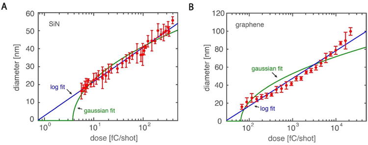
By adjusting the electron dose used in the patterning, we are able to vary the size of the nanopores formed, as shown in Fig. 3, where resulting diameter of the nanopore is plotted against the electron-beam dose used per shot of e-beam exposure, for both the SiN (Fig. 3A) and graphene nanopores (Fig. 3B). The smallest nanopore made was approximately 16±2 nm, both for SiN and graphene. Nanopores fabricated show similar variation in size (standard deviation is <10%) in both SiN and graphene. Because these values are similar and close to the size of the beamspot used (∼15 nm), we speculate that the electron-beam spot size limits the resolution and hence it may be possible to fabricate smaller pores using a smaller spot size. By varying the electron-beam dose only, we obtained a range of nanopore sizes from 16 to >100 nm, though in principle even bigger sized pores can be produced by rasterizing a larger area with multiple shots of e-beam exposure.
Figure 3. Single-shot nanopore diameter versus electron-beam dose.

The solid blue line is an empirical logarithmic fit (A-SIN: , B- Graphene : ), the green curve is a fit assuming a Gaussian dependence of dose on diameter (A-SiN: , B-Graphene: ). Error bars are the standard deviation , values are calculated using the standard error of the mean for each datapoint.
Interestingly, we find that the diameter of the resulting nanopore follows an empirical logarithmic relationship to the electron dose used for both SiN and graphene:
where d is the nanopore diameter, D is the total electron dose, and A and B are fit parameters. A least-squares fit of Eqn. 1 to the red data points is plotted as a solid blue line in Fig. 3 and shows good agreement with the data (SiN: , graphene: ). The specific values of the fit parameters A and B are not universal and will depend on experimental factors, such as the membrane material, resist thickness and the electron accelerating voltage. A different dependence results if patterning is performed on a thick substrate since electron backscatter from the substrate will be the dominant contribution to the exposure30. The agreement between the data and relationship is somewhat surprising as a more complex dependence is expected if one assumes that the nanopore size is merely set by the point spread function (PSF) of the electron beam29. This dependency can be modelled by assuming the resist only develops after receiving a local electron dose per unit area D̃ larger than some threshold value of the dose DT. Using a Gaussian PSF to describe the electron beam profile (D̃(r) ∝ De−γr2, where r is the distance from the center of the electron beam, D is the total dose, and γ is a fit parameter) and setting DT = D̃(d), a dependency of the diameter on the total dose can be extracted. This dependency is plotted as a green line in Fig. 3 and does not explain the trend well. Only moderate agreement between data (SiN , graphene: ) is obtained.
One might wonder if the use of PMMA as a resist will set a maximum size for the nanopore size that can be fabricated, as it is known that PMMA will behave as a negative-tone resist at high doses35 (>100fC). This is however not the case, as at high-dose exposure, the resist in the tail of the beam will still be exposed to a low dose. This leads to a donut-shaped cut in the resist after development which will create a hole in the membrane after pattern transfer by RIE. Moreover, standard resist patterning (rastering) can be used for nanopores larger than 50 nm in diameter or for large nanopores of different shapes.
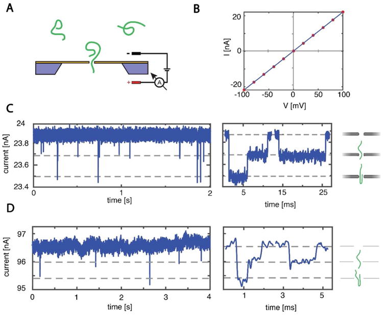
To show that the SiN and graphene nanopores created using this method can be used for the detection of DNA, we performed double-stranded DNA (lambda-DNA, 48.5kbp) translocation experiments on these nanopores. A schematic of a typical nanopore experiment is shown in Fig. 4A, where DNA molecules added to the negatively-biased cis compartment of the flow cell are electrophoretically driven through the nanopore and detected by a change in ionic current through the pore. Fig. 4 shows examples of DNA translocations through a 18 nm graphene nanopore, fabricated using a dose of 88 fC, and a 25 nm SiN nanopore, fabricated using a dose of 15 fC. DNA translocation experiments were done in a PEEK (Polyether ether ketone) flow cell in 2M LiCl (buffered with 20mM Tris-Cl, 2mM EDTA, pH 8) and we used Ag/AgCl electrodes and an Axopatch 200B amplifier (Molecular Devices) for current detection. To wet the graphene nanopore, we incubated the chip in the flow cell with a mixture of equal parts ethanol and water for 30 min.
Figure 4. DNA translocations through RIE-fabricated SiN and graphene nanopores.

(A) Schematic illustration of a DNA translocation experiment. (B) IV-curve of a 25 nm SiN nanopore with a resistance of 4.5 MΩ, with the corresponding linear fit. (C) Left: Current time trace through a SiN nanopore of 25 nm (4.5 MΩ). Data was taken at 100 mV in 2M LiCl and low-pass filtered at 10 kHz. Right: zooms of DNA translocations, showing a folded and a linear translocation. (D) Left: Current time trace through a graphene nanopore of 18 nm (4.0 MΩ). Data was taken at 500 mV in 2M LiCl and low-pass filtered at 5 kHz. The large driving voltage was used to enhance the DNA translocation rate. Right: zooms of DNA translocations, showing a folded and a linear translocation.
Figure 4B shows the linear I-V curve of the SiN nanopore with a resistance of 4.5 MΩ. This compares well with the expected resistance of 3.9 MΩ for a 25 nm nanopore, calculated using a measured buffer conductivity of 13.8 nS/m and an effective membrane thickness of 6.7 nm. After adding lambda-DNA to the cis chamber at a concentration of 10 ng/μL, transient current blockades could be clearly discerned, as shown in the first panel of Fig. 4C. The translocations show excellent signal-to-noise characteristics, illustrated by the zooms in the right panel of Fig. 4C of two such DNA translocations, one molecule translocating in a linear fashion (right) and one in a folded conformation (left). The double-strand DNA conductance blockade of 1.8 nS (N = 580) matches the expected value of 1.8 nS well. The normalized current power spectral density can be found in the SI.
Fig. 4D shows example DNA translocations through a 18 nm graphene nanopore. The nanopore had a resistance of 4.9 MΩ, which agrees reasonably well with the expected 4.2 MΩ using an effective membrane thickness of 0.6 nm36-38. We used a high driving voltage of 500 mV, to enhance the low capture rates often observed in bare graphene nanopores39. The current time trace shows considerable low-frequency current noise, similar to what was observed for TEM-drilled graphene nanopores40 (see SI). Analysis41 of all detected events at 500 mV (N = 59) show a blockade levels of ∼1.0 nS. This is markedly lower than the theoretically expected blockade of 5.6 nS from a dsDNA strand in a 18 nm graphene nanopore42, but the discrepancy is consistent with previous work on TEM-drilled graphene nanopores which gave values of 1.5 nS for similar sized pores34. Graphene nanopores drilled using this RIE based method suffer from the same challenges as graphene nanopores drilled using TEM. These challenges include limited statistics and current-signal resolving power caused by graphene-DNA interactions43 and high 1/f noise40. Fortunately, these issues can be mitigated by reducing the freestanding area and using a molecular coating of the graphene39.
Summarizing, these nanopores created using EBL with RIE show sensing characteristics that are on par with their TEM-drilled counterparts.
Conclusions
In conclusion, we have developed a facile method for rapid, flexible, and large-scale nanopore manufacturing in freestanding SiN and graphene membranes using electron-beam lithography with reactive ion etching which are very commonly available fabrication techniques. As the nanopore is created in the final step of the fabrication, our approach is extremely versatile and can in principle by used on any substrate, in particular 2D materials that require a transfer step. By adjusting the electron-beam dose, the diameter of the nanopore can accurately be controlled with a high-level of uniformity and precision. Furthermore, we demonstrate that the nanopores fabricated with this method show single-molecule sensing performances equivalent to their TEM drilled predecessors. The ease of the method allows for patterning large intact areas of freestanding 2D materials like graphene with a clearly defined array of nanopores. We expect that this technique will also find a range of applications beyond mere nanopore sensing, such as filtration with nano-sieves and graphene gas sensing.
Supplementary Material
Acknowledgments
We like to thank Meng-Yue Wu for TEM imaging, Stephanie Heerema, Xin Shi, and Sergii Pud for the valuable discussions. This work was supported by the National Human Genome Research Institute of the National Institute of Health under Award Number R01-HG007406, ERC Advanced Grant SynDiv (No. 669598), and the Netherlands Organization of Scientific Research (NWO/OCW) as part of the Frontiers of Nanoscience Program.
References
- 1.Arjmandi-Tash H, Belyaeva LA, Schneider GF. Chemical Society Reviews. 2016;45(3):476–493. doi: 10.1039/c5cs00512d. [DOI] [PMC free article] [PubMed] [Google Scholar]
- 2.Aghigh A, Alizadeh V, Wong HY, Islam MS, Amin N, Zaman M. Desalination. 2015;365:389–397. [Google Scholar]
- 3.Dekker C. Nature nanotechnology. 2007;2(4):209–215. doi: 10.1038/nnano.2007.27. [DOI] [PubMed] [Google Scholar]
- 4.Feng J, Graf M, Liu K, Ovchinnikov D, Dumcenco D, Heiranian M, Nandigana V, Aluru NR, Kis A, Radenovic A. Nature. 2016;536(7615):197–200. doi: 10.1038/nature18593. [DOI] [PubMed] [Google Scholar]
- 5.Heerema SJ, Dekker C. Nature nanotechnology. 2016;11(2):127–136. doi: 10.1038/nnano.2015.307. [DOI] [PubMed] [Google Scholar]
- 6.Chen J, Li C, Shi G. The journal of physical chemistry letters. 2013;4(8):1244–1253. doi: 10.1021/jz400160k. [DOI] [PubMed] [Google Scholar]
- 7.Jiang De, Cooper VR, Dai S. Nano letters. 2009;9(12):4019–4024. doi: 10.1021/nl9021946. [DOI] [PubMed] [Google Scholar]
- 8.Muthukumar M, Plesa C, Dekker C. Physics Today. 2015;68(8):40. [Google Scholar]
- 9.Plesa C, Ruitenberg JW, Witteveen MJ, Dekker C. Nano Lett. 2015;15(5):3153–3158. doi: 10.1021/acs.nanolett.5b00249. [DOI] [PubMed] [Google Scholar]
- 10.Raillon C, Cousin P, Traversi F, Garcia-Cordero E, Hernandez N, Radenovic A. Nano letters. 2012;12(EPFL-ARTICLE-176020):1157–1164. doi: 10.1021/nl3002827. [DOI] [PubMed] [Google Scholar]
- 11.Smeets R, Kowalczyk S, Hall A, Dekker N, Dekker C. Nano letters. 2008;9(9):3089–3095. doi: 10.1021/nl803189k. [DOI] [PubMed] [Google Scholar]
- 12.Marshall MM, Ruzicka J, Zahid OK, Henrich VC, Taylor EW, Hall AR. Langmuir. 2015;31(15):4582–4588. doi: 10.1021/acs.langmuir.5b00457. [DOI] [PubMed] [Google Scholar]
- 13.Japrung D, Bahrami A, Nadzeyka A, Peto L, Bauerdick S, Edel JB, Albrecht T. The journal of physical chemistry B. 2014;118(40):11605–11612. doi: 10.1021/jp506832u. [DOI] [PubMed] [Google Scholar]
- 14.Storm A, Chen J, Ling X, Zandbergen H, Dekker C. Nature materials. 2003;2(8):537–540. doi: 10.1038/nmat941. [DOI] [PubMed] [Google Scholar]
- 15.Kim MJ, Wanunu M, Bell DC, Meller A. Advanced materials. 2006;18(23):3149–3153. [Google Scholar]
- 16.Van den Hout M, Hall AR, Wu MY, Zandbergen HW, Dekker C, Dekker NH. Nanotechnology. 2010;21(11):115304. doi: 10.1088/0957-4484/21/11/115304. [DOI] [PubMed] [Google Scholar]
- 17.Deng T, Li M, Wang Y, Liu Z. Science bulletin. 2015;60(3):304–319. [Google Scholar]
- 18.Xu Q, Wu MY, Schneider GF, Houben L, Malladi SK, Dekker C, Yucelen E, Dunin-Borkowski RE, Zandbergen HW. Acs Nano. 2013;7(2):1566–1572. doi: 10.1021/nn3053582. [DOI] [PubMed] [Google Scholar]
- 19.Yang J, Ferranti DC, Stern LA, Sanford CA, Huang J, Ren Z, Qin LC, Hall AR. Nanotechnology. 2011;22(28):285310. doi: 10.1088/0957-4484/22/28/285310. [DOI] [PubMed] [Google Scholar]
- 20.Deng Y, Huang Q, Zhao Y, Zhou D, Ying C, Wang D. Nanotechnology. 2016;28(4):045302. doi: 10.1088/1361-6528/28/4/045302. [DOI] [PubMed] [Google Scholar]
- 21.Kwok H, Briggs K, Tabard-Cossa V. PloS one. 2014;9(3):e92880. doi: 10.1371/journal.pone.0092880. [DOI] [PMC free article] [PubMed] [Google Scholar]
- 22.Kuan AT, Lu B, Xie P, Szalay T, Golovchenko JA. Applied physics letters. 2015;106(20):203109. doi: 10.1063/1.4921620. [DOI] [PMC free article] [PubMed] [Google Scholar]
- 23.Zrehen A, Gilboa T, Meller A. Nanoscale. 2017;9(42):16437–16445. doi: 10.1039/c7nr02629c. [DOI] [PubMed] [Google Scholar]
- 24.Park SR, Peng H, Ling XS. Small. 2007;3(1):116–119. doi: 10.1002/smll.200600268. [DOI] [PubMed] [Google Scholar]
- 25.Deng T, Chen J, Wu C, Liu Z. ECS journal of solid state science and technology. 2013;2(11):P419–P422. [Google Scholar]
- 26.Yasuda K, Ghicov A, Nohira T, Kani N, Hagiwara R, Schmuki P. Electrochemical and Solid-State Letters. 2008;11(9):C51–C54. [Google Scholar]
- 27.Han A, Creus M, Schürmann G, Linder V, Ward TR, de Rooij NF, Staufer U. Analytical chemistry. 2008;80(12):4651–4658. doi: 10.1021/ac7025207. [DOI] [PubMed] [Google Scholar]
- 28.Bai J, Wang D, Nam Sw, Peng H, Bruce R, Gignac L, Brink M, Kratschmer E, Rossnagel S, Waggoner P. Nanoscale. 2014;6(15):8900–8906. doi: 10.1039/c3nr06723h. [DOI] [PubMed] [Google Scholar]
- 29.Ahmadi AG, Nair S. Microelectronic Engineering. 2013;112:149–156. [Google Scholar]
- 30.Wei R, Pedone D, Zürner A, Döblinger M, Rant U. Small. 2010;6(13):1406–1414. doi: 10.1002/smll.201000253. [DOI] [PubMed] [Google Scholar]
- 31.Adesida I, Everhart T, Shimizu R. Journal of Vacuum Science and Technology. 1979;16(6):1743–1748. [Google Scholar]
- 32.Howorka S, Siwy Z. Chemical Society Reviews. 2009;38(8):2360–2384. doi: 10.1039/b813796j. [DOI] [PubMed] [Google Scholar]
- 33.Dolleman RJ, Davidovikj D, Cartamil-Bueno SJ, van der Zant HS, Steeneken PG. Nano letters. 2015;16(1):568–571. doi: 10.1021/acs.nanolett.5b04251. [DOI] [PubMed] [Google Scholar]
- 34.Schneider GF, Kowalczyk SW, Calado VE, Pandraud G, Zandbergen HW, Vandersypen LM, Dekker C. Nano letters. 2010;10(8):3163–3167. doi: 10.1021/nl102069z. [DOI] [PubMed] [Google Scholar]
- 35.Duan H, Winston D, Yang JK, Cord BM, Manfrinato VR, Berggren KK. Journal of Vacuum Science & Technology B. 2010;28(6):C6C58–C6C62. [Google Scholar]
- 36.Kowalczyk SW, Grosberg AY, Rabin Y, Dekker C. Nanotechnology. 2011;22(31):315101. doi: 10.1088/0957-4484/22/31/315101. [DOI] [PubMed] [Google Scholar]
- 37.Heerema SJ, Schneider GF, Rozemuller M, Vicarelli L, Zandbergen HW, Dekker C. Nanotechnology. 2015;26(7):074001. doi: 10.1088/0957-4484/26/7/074001. [DOI] [PubMed] [Google Scholar]
- 38.Rollings RC, Kuan AT, Golovchenko JA. Nature communications. 2016;7 doi: 10.1038/ncomms11408. [DOI] [PMC free article] [PubMed] [Google Scholar]
- 39.Schneider GF, Xu Q, Luik S, Hage S, Spoor JN, Malladi S, Zandbergen H, Dekker C. Nature. 2013;4:2619. doi: 10.1038/ncomms3619. [DOI] [PubMed] [Google Scholar]
- 40.Heerema S, Schneider G, Rozemuller M, Vicarelli L, Zandbergen H, Dekker C. Nanotechnology. 2015;26(7):074001. doi: 10.1088/0957-4484/26/7/074001. [DOI] [PubMed] [Google Scholar]
- 41.Plesa C, Dekker C. Nanotechnology. 2015;26(8):084003. doi: 10.1088/0957-4484/26/8/084003. [DOI] [PubMed] [Google Scholar]
- 42.Carlsen AT, Zahid OK, Ruzicka J, Taylor EW, Hall AR. Acs Nano. 2014;8(5):4754–4760. doi: 10.1021/nn501694n. [DOI] [PubMed] [Google Scholar]
- 43.Kabiri Y, Ananth AN, van der Torre J, Katan A, Hong JY, Malladi S, Kong J, Zandbergen H, Dekker C. Small. 2017 doi: 10.1002/smll.201700876. [DOI] [PubMed] [Google Scholar]
Associated Data
This section collects any data citations, data availability statements, or supplementary materials included in this article.


